EP0660399A2 - Ball-grid-array integrated circuit package with thermal conductivity - Google Patents
Ball-grid-array integrated circuit package with thermal conductivity Download PDFInfo
- Publication number
- EP0660399A2 EP0660399A2 EP94308577A EP94308577A EP0660399A2 EP 0660399 A2 EP0660399 A2 EP 0660399A2 EP 94308577 A EP94308577 A EP 94308577A EP 94308577 A EP94308577 A EP 94308577A EP 0660399 A2 EP0660399 A2 EP 0660399A2
- Authority
- EP
- European Patent Office
- Prior art keywords
- substrate
- integrated circuit
- slug
- chip
- packaged integrated
- Prior art date
- Legal status (The legal status is an assumption and is not a legal conclusion. Google has not performed a legal analysis and makes no representation as to the accuracy of the status listed.)
- Withdrawn
Links
Images
Classifications
-
- H10W70/635—
-
- H—ELECTRICITY
- H05—ELECTRIC TECHNIQUES NOT OTHERWISE PROVIDED FOR
- H05K—PRINTED CIRCUITS; CASINGS OR CONSTRUCTIONAL DETAILS OF ELECTRIC APPARATUS; MANUFACTURE OF ASSEMBLAGES OF ELECTRICAL COMPONENTS
- H05K3/00—Apparatus or processes for manufacturing printed circuits
- H05K3/30—Assembling printed circuits with electric components, e.g. with resistor
- H05K3/303—Surface mounted components, e.g. affixing before soldering, aligning means, spacing means
-
- H—ELECTRICITY
- H05—ELECTRIC TECHNIQUES NOT OTHERWISE PROVIDED FOR
- H05K—PRINTED CIRCUITS; CASINGS OR CONSTRUCTIONAL DETAILS OF ELECTRIC APPARATUS; MANUFACTURE OF ASSEMBLAGES OF ELECTRICAL COMPONENTS
- H05K3/00—Apparatus or processes for manufacturing printed circuits
- H05K3/30—Assembling printed circuits with electric components, e.g. with resistor
- H05K3/32—Assembling printed circuits with electric components, e.g. with resistor electrically connecting electric components or wires to printed circuits
- H05K3/34—Assembling printed circuits with electric components, e.g. with resistor electrically connecting electric components or wires to printed circuits by soldering
- H05K3/341—Surface mounted components
- H05K3/3431—Leadless components
- H05K3/3436—Leadless components having an array of bottom contacts, e.g. pad grid array or ball grid array components
-
- H10W40/228—
-
- H10W40/778—
-
- H10W74/117—
-
- H10W90/701—
-
- H—ELECTRICITY
- H05—ELECTRIC TECHNIQUES NOT OTHERWISE PROVIDED FOR
- H05K—PRINTED CIRCUITS; CASINGS OR CONSTRUCTIONAL DETAILS OF ELECTRIC APPARATUS; MANUFACTURE OF ASSEMBLAGES OF ELECTRICAL COMPONENTS
- H05K1/00—Printed circuits
- H05K1/02—Details
- H05K1/0201—Thermal arrangements, e.g. for cooling, heating or preventing overheating
- H05K1/0203—Cooling of mounted components
-
- H—ELECTRICITY
- H05—ELECTRIC TECHNIQUES NOT OTHERWISE PROVIDED FOR
- H05K—PRINTED CIRCUITS; CASINGS OR CONSTRUCTIONAL DETAILS OF ELECTRIC APPARATUS; MANUFACTURE OF ASSEMBLAGES OF ELECTRICAL COMPONENTS
- H05K2201/00—Indexing scheme relating to printed circuits covered by H05K1/00
- H05K2201/09—Shape and layout
- H05K2201/09209—Shape and layout details of conductors
- H05K2201/09654—Shape and layout details of conductors covering at least two types of conductors provided for in H05K2201/09218 - H05K2201/095
- H05K2201/09781—Dummy conductors, i.e. not used for normal transport of current; Dummy electrodes of components
-
- H—ELECTRICITY
- H05—ELECTRIC TECHNIQUES NOT OTHERWISE PROVIDED FOR
- H05K—PRINTED CIRCUITS; CASINGS OR CONSTRUCTIONAL DETAILS OF ELECTRIC APPARATUS; MANUFACTURE OF ASSEMBLAGES OF ELECTRICAL COMPONENTS
- H05K2201/00—Indexing scheme relating to printed circuits covered by H05K1/00
- H05K2201/10—Details of components or other objects attached to or integrated in a printed circuit board
- H05K2201/10613—Details of electrical connections of non-printed components, e.g. special leads
- H05K2201/10621—Components characterised by their electrical contacts
- H05K2201/10734—Ball grid array [BGA]; Bump grid array
-
- H—ELECTRICITY
- H05—ELECTRIC TECHNIQUES NOT OTHERWISE PROVIDED FOR
- H05K—PRINTED CIRCUITS; CASINGS OR CONSTRUCTIONAL DETAILS OF ELECTRIC APPARATUS; MANUFACTURE OF ASSEMBLAGES OF ELECTRICAL COMPONENTS
- H05K2201/00—Indexing scheme relating to printed circuits covered by H05K1/00
- H05K2201/10—Details of components or other objects attached to or integrated in a printed circuit board
- H05K2201/10613—Details of electrical connections of non-printed components, e.g. special leads
- H05K2201/10954—Other details of electrical connections
- H05K2201/10969—Metallic case or integral heatsink of component electrically connected to a pad on PCB
-
- H—ELECTRICITY
- H05—ELECTRIC TECHNIQUES NOT OTHERWISE PROVIDED FOR
- H05K—PRINTED CIRCUITS; CASINGS OR CONSTRUCTIONAL DETAILS OF ELECTRIC APPARATUS; MANUFACTURE OF ASSEMBLAGES OF ELECTRICAL COMPONENTS
- H05K2203/00—Indexing scheme relating to apparatus or processes for manufacturing printed circuits covered by H05K3/00
- H05K2203/04—Soldering or other types of metallurgic bonding
- H05K2203/041—Solder preforms in the shape of solder balls
-
- H—ELECTRICITY
- H05—ELECTRIC TECHNIQUES NOT OTHERWISE PROVIDED FOR
- H05K—PRINTED CIRCUITS; CASINGS OR CONSTRUCTIONAL DETAILS OF ELECTRIC APPARATUS; MANUFACTURE OF ASSEMBLAGES OF ELECTRICAL COMPONENTS
- H05K2203/00—Indexing scheme relating to apparatus or processes for manufacturing printed circuits covered by H05K3/00
- H05K2203/04—Soldering or other types of metallurgic bonding
- H05K2203/0465—Shape of solder, e.g. differing from spherical shape, different shapes due to different solder pads
-
- H—ELECTRICITY
- H05—ELECTRIC TECHNIQUES NOT OTHERWISE PROVIDED FOR
- H05K—PRINTED CIRCUITS; CASINGS OR CONSTRUCTIONAL DETAILS OF ELECTRIC APPARATUS; MANUFACTURE OF ASSEMBLAGES OF ELECTRICAL COMPONENTS
- H05K3/00—Apparatus or processes for manufacturing printed circuits
- H05K3/30—Assembling printed circuits with electric components, e.g. with resistor
- H05K3/32—Assembling printed circuits with electric components, e.g. with resistor electrically connecting electric components or wires to printed circuits
- H05K3/34—Assembling printed circuits with electric components, e.g. with resistor electrically connecting electric components or wires to printed circuits by soldering
- H05K3/341—Surface mounted components
- H05K3/3431—Leadless components
-
- H10W70/682—
-
- H10W70/685—
-
- H10W72/07554—
-
- H10W72/547—
-
- H10W74/00—
-
- H10W74/142—
-
- H10W90/737—
-
- H10W90/754—
-
- Y—GENERAL TAGGING OF NEW TECHNOLOGICAL DEVELOPMENTS; GENERAL TAGGING OF CROSS-SECTIONAL TECHNOLOGIES SPANNING OVER SEVERAL SECTIONS OF THE IPC; TECHNICAL SUBJECTS COVERED BY FORMER USPC CROSS-REFERENCE ART COLLECTIONS [XRACs] AND DIGESTS
- Y02—TECHNOLOGIES OR APPLICATIONS FOR MITIGATION OR ADAPTATION AGAINST CLIMATE CHANGE
- Y02P—CLIMATE CHANGE MITIGATION TECHNOLOGIES IN THE PRODUCTION OR PROCESSING OF GOODS
- Y02P70/00—Climate change mitigation technologies in the production process for final industrial or consumer products
- Y02P70/50—Manufacturing or production processes characterised by the final manufactured product
-
- Y—GENERAL TAGGING OF NEW TECHNOLOGICAL DEVELOPMENTS; GENERAL TAGGING OF CROSS-SECTIONAL TECHNOLOGIES SPANNING OVER SEVERAL SECTIONS OF THE IPC; TECHNICAL SUBJECTS COVERED BY FORMER USPC CROSS-REFERENCE ART COLLECTIONS [XRACs] AND DIGESTS
- Y10—TECHNICAL SUBJECTS COVERED BY FORMER USPC
- Y10T—TECHNICAL SUBJECTS COVERED BY FORMER US CLASSIFICATION
- Y10T29/00—Metal working
- Y10T29/49—Method of mechanical manufacture
- Y10T29/49002—Electrical device making
- Y10T29/49117—Conductor or circuit manufacturing
- Y10T29/49124—On flat or curved insulated base, e.g., printed circuit, etc.
- Y10T29/4913—Assembling to base an electrical component, e.g., capacitor, etc.
- Y10T29/49144—Assembling to base an electrical component, e.g., capacitor, etc. by metal fusion
Definitions
- This invention is in the field of semiconductor device packages, and is more particularly directed to thermal conduction techniques therein.
- BGA packages have recently become popular in the field.
- Conventional BGA packages are similar in layout and arrangement to the pin-grid-array (PGA) packages, in providing a rectangular or square array of connections on the underside of the integrated circuit package.
- PGA packages instead of the pin connectors used in PGA packages, however, BGA packages utilize a solder ball located at each connector location.
- the BGA package is attached to a printed circuit board by reflowing the solder balls to make connection to conductors at the surface of the printed circuit board.
- the BGA package provides the important advantage of being self-aligning, as the surface tension of the solder will tend to pull the BGA package into proper alignment with the corresponding conductors on the printed circuit board.
- BGA integrated circuit packages of various types are known, including those of both the “cavity-up” and the “cavity-down” type.
- Conventional cavity-up BGA,packages mount the integrated circuit chip face-up into a cavity (or onto the surface) of the package substrate, attach wire bonds between the package and the chip on this top side, and then either transfer mold or otherwise dispense a plastic over the chip and bond wires to provide environmental protection to the chip and wires.
- the solder balls are provided on the side of the substrate opposite the chip, and the packaged chip is then mounted to the system printed circuit board. It is known to use plated vias through the substrate at locations underlying the chip, but that are offset from conductors on the printed circuit board to which the packaged chip is mounted, to provide thermal conduction from the chip to its external environment.
- BGA ball-grid-array
- the invention may be implemented in a ball-grid-array (BGA) package of the cavity-up orientation.
- a thermally conductive slug for example formed of copper, is inserted into a cavity of the package substrate; the substrate may itself be formed of a printed circuit board or ceramic substrate of the single, double, or multiple layer type.
- a surface of the slug is exposed on the underside of the substrate.
- the integrated circuit chip is attached to the slug, and bonds are made between the bond pads on the chip and the package conductors, followed by encapsulation of the chip by molding or dispensing of a plastic.
- Solder balls are attached on the underside of the package at locations corresponding to the terminals of the package, and also at locations on the exposed surface of the slug.
- thermal connection is made between the slug and system circuit board conductors, along with electrical connection of the other solder ball connectors to their respective system circuit board terminals.
- the slug thus provides direct thermal conduction between the chip and the system circuit board, to take advantage of the thermal conductivity of the system circuit board in conducting heat from the chip.
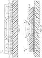
- Figure 1 is a cross-sectional illustration of an integrated circuit package according to the preferred embodiment of the present invention.
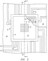
- Figure 2 is a plan view of the integrated circuit package according to Figure 1, including a cutaway portion.
- Figure 3 is a cross-sectional illustration of an integrated circuit package according to an alternative preferred embodiment of the present invention.
- packaged integrated circuit 8 according to a first preferred embodiment of the invention will now be described in detail. While packaged integrated circuit 8 according to this embodiment of the invention is shown in each of Figures 1 and 2 as already attached to system circuit board 20, it is to be understood by those of ordinary skill in the art that packaged integrated circuit 8 according to this embodiment of the invention will often individually manufactured and sold, with the purchaser performing the installation of packaged integrated circuit 8 to system circuit board 20 in a computer or other end equipment.
- the active element of packaged integrated circuit 8 is semiconductor chip 10, which is a solid-state integrated circuit device such as a microprocessor, memory, logic device, analog device or other electronic function implemented in a single-chip integrated circuit, as known in the art. According to this embodiment of the invention, chip 10 is attached on its bottom (inactive) surface to conductive slug 12, mounted within substrate 14.
- Substrate 14 may be a ceramic substrate, printed circuit board, or other similar substrate having conductors 24 thereupon or therewithin (see Figure 2) for carrying electrical signals to and from chip 10, and having an opening or receptacle therein within which conductive slug 12 is mounted.
- Bond wires 15 connect conductors 24 to bond pads on chip 10 in the conventional manner.
- Plated-through vias 19 make connection between conductors 24 on the top surface of substrate 14 and solder balls 18 on the lower surface of substrate 14.
- solder balls 18 are arranged in the conventional ball-grid-array manner, and correspond to lands or other surface conductors 23 (see Figure 2) on the top surface of system circuit board 20 to which packaged integrated circuit 8 is to be mounted.
- Conductive slug 12 is preferably formed of a material with high thermal conductivity, so that heat from chip 10 may be readily conducted therethrough. In addition, if electrical connection is to be made to the body of chip 10, conductive slug 12 is also preferably electrically conductive. The preferred material for conductive slug 12 is believed to be copper, but other materials known in the art to be thermally conductive and, if desired, electrically conductive, may alternatively be used for slug 12.
- Solder balls 18 are also disposed in an array manner beneath and in contact with slug 12, for providing thermal connection between slug 12 and a thermal conductor in system circuit board 20.
- conductive trace 22 is a wide trace on system circuit board 20 that is capable of conducting heat from chip 10 via slug 12 and solder balls 18.
- slug 12 may be connected by solder balls 18 to a ground plane within system circuit board 20. In either case, conductor 22 or the ground plane may be biased to ground or another substrate bias voltage, in which case slug 12 will also provide proper grounding for chip 10.
- packaged integrated circuit 8 begins with the insertion of slug 12 into the corresponding cavity of substrate 14; slug 12 is preferably epoxied into this cavity for mechanical integrity.
- Chip 10 is then mounted to the top surface of slug 12 by conventional die attach techniques, such as a conductive epoxy or eutectic mount.
- Bond wires 15 are then attached between substrate 14 and chip 10 by conventional techniques, such as thermocompression or ultrasonic bonding.
- encapsulant 16 is formed over chip 10 and wires 15 in the conventional manner.
- encapsulate 16 is formed by conventional transfer molding; alternatively, encapsulant 16 may be "globbed" over chip 10 and substrate 14 by dispensation and curing, in the conventional manner.
- Solder balls 18 are formed on the underside of substrate 14 and slug 12, in the conventional manner, for example by way of a solder mask (not shown) on the underside of substrate 14.
- packaged integrated circuit 8 Upon completion of the construction of packaged integrated circuit 8, and any desired electrical testing in packaged form, packaged integrated circuit 8 is ready for mounting to system circuit board 20. Mounting of packaged integrated circuit 8 is preferably done by way of wave soldering or other conventional technique for the surface mounting of BGA packages to circuit boards.
- Figure 3 illustrates, in cross-section, packaged integrated circuit 50 according to a second embodiment of the invention.
- packaged integrated circuit 50 includes chip 30 mounted upon thermally conductive slug 32.
- Slug 32 is disposed within substrate 34, which in this example is a multilayer circuit board including multiple levels of conductors therewithin.
- the multiple levels of conductors in substrate 34 are presented by multiple shells of lands, as indicated by the stepped arrangement near the chip cavity of substrate 34.
- a cutout is provided on the underside of substrate 34, to provide lateral surfaces 33 to which slug 32 may be epoxied or otherwise securely fastened.
- slug 32 includes a smaller portion protruding through substrate 34, to which chip 30 is mounted, with larger exposure on the underside of substrate 34.
- This construction allows for slug 32 to be the proper size for receipt of chip 30 on its top size, providing the maximum area for the arrangement of bond wire lands on substrate 34 with minimum wire length, while maximizing the surface area of thermal conduction on the underside.
- Bond wires 35 electrically connect conductors (not shown) in substrate 34 to pads on the surface of chip 30, for connection to the multiple planes of conductors.
- encapsulant 36 is disposed over the cavity of substrate 34, and thus over chip 30 and wires 35.
- Encapsulant 36 according to this embodiment of the invention is dispensed by way of a syringe or other liquid dispenser, and is then cured in the conventional manner for so-called "chip-on-board" construction.
- Solder balls 38 are attached to lands on the bottom surface of substrate 34. Vias (not shown) are provided within substrate 34 to provide electrical connection to the conductors in the substrate. Solder mask 37 on the underside of substrate 34 assists in defining the location of solder balls 38, during their formation in the conventional manner.
- packaged integrated circuit 50 is attached to system circuit board 40 by way of infrared (IR) solder reflow or other conventional surface mount technology.
- IR infrared
- Those solder balls 38 that are in contact with slug 32 connect to a thermal conductor within system circuit board 40, thus providing a path of relatively low thermal resistance between chip 30 and system circuit board 40 through solder balls 38 and slug 32.
- an integrated circuit package which has a high thermal conductivity path is provided between the active integrated circuit therewithin and the system circuit board to which the packaged integrated circuit is mounted.
- This enables the advantageous use of the system circuit board thermal conductivity to remove heat from the integrated circuit chip via conduction, and as such is suitable for use in zero-air-flow environments such as notebook-size computers, hand-held computing devices such as PDAs, and the like.
Landscapes
- Engineering & Computer Science (AREA)
- Manufacturing & Machinery (AREA)
- Microelectronics & Electronic Packaging (AREA)
- Cooling Or The Like Of Semiconductors Or Solid State Devices (AREA)
Applications Claiming Priority (2)
| Application Number | Priority Date | Filing Date | Title |
|---|---|---|---|
| US17061393A | 1993-12-20 | 1993-12-20 | |
| US170613 | 1993-12-20 |
Publications (2)
| Publication Number | Publication Date |
|---|---|
| EP0660399A2 true EP0660399A2 (en) | 1995-06-28 |
| EP0660399A3 EP0660399A3 (esLanguage) | 1995-07-26 |
Family
ID=22620603
Family Applications (1)
| Application Number | Title | Priority Date | Filing Date |
|---|---|---|---|
| EP94308577A Withdrawn EP0660399A2 (en) | 1993-12-20 | 1994-11-21 | Ball-grid-array integrated circuit package with thermal conductivity |
Country Status (3)
| Country | Link |
|---|---|
| US (2) | US5991156A (esLanguage) |
| EP (1) | EP0660399A2 (esLanguage) |
| JP (1) | JPH07211816A (esLanguage) |
Cited By (4)
| Publication number | Priority date | Publication date | Assignee | Title |
|---|---|---|---|---|
| EP0690500A1 (en) * | 1994-06-30 | 1996-01-03 | STMicroelectronics, Inc. | Ball-grid-array integrated circuit package with solder-connected thermal conductor |
| WO1997026605A1 (en) * | 1996-01-22 | 1997-07-24 | Silicon Graphics, Inc. | Processor-inclusive memory module |
| US5867419A (en) * | 1997-01-27 | 1999-02-02 | Silicon Graphics, Inc. | Processor-inclusive memory module |
| EP3706165A1 (en) * | 2019-03-04 | 2020-09-09 | INTEL Corporation | Nested architectures for enhanced heterogeneous integration |
Families Citing this family (75)
| Publication number | Priority date | Publication date | Assignee | Title |
|---|---|---|---|---|
| US6686226B1 (en) | 1994-02-10 | 2004-02-03 | Hitachi, Ltd. | Method of manufacturing a semiconductor device a ball grid array package structure using a supporting frame |
| TW344109B (en) * | 1994-02-10 | 1998-11-01 | Hitachi Ltd | Methods of making semiconductor devices |
| NL9500238A (nl) * | 1995-02-09 | 1996-09-02 | Fico Bv | Omhulinrichting met compensatie-element. |
| JP3793628B2 (ja) * | 1997-01-20 | 2006-07-05 | 沖電気工業株式会社 | 樹脂封止型半導体装置 |
| DE19750306A1 (de) * | 1997-11-13 | 1999-05-20 | Bosch Gmbh Robert | Elektronisches Steuergerät |
| US6060777A (en) * | 1998-07-21 | 2000-05-09 | Intel Corporation | Underside heat slug for ball grid array packages |
| US6424034B1 (en) * | 1998-08-31 | 2002-07-23 | Micron Technology, Inc. | High performance packaging for microprocessors and DRAM chips which minimizes timing skews |
| JP4142170B2 (ja) * | 1998-09-25 | 2008-08-27 | 新電元工業株式会社 | 電気装置 |
| US6138894A (en) * | 1998-11-25 | 2000-10-31 | Intermedics Inc. | Method for coupling a circuit component to a substrate |
| US6321175B1 (en) * | 1998-12-21 | 2001-11-20 | Intel Corporation | Thermal sensing of multiple integrated circuits |
| US6844253B2 (en) * | 1999-02-19 | 2005-01-18 | Micron Technology, Inc. | Selective deposition of solder ball contacts |
| US6435396B1 (en) * | 2000-04-10 | 2002-08-20 | Micron Technology, Inc. | Print head for ejecting liquid droplets |
| US6878396B2 (en) * | 2000-04-10 | 2005-04-12 | Micron Technology, Inc. | Micro C-4 semiconductor die and method for depositing connection sites thereon |
| US6249434B1 (en) * | 2000-06-20 | 2001-06-19 | Adc Telecommunications, Inc. | Surface mounted conduction heat sink |
| US6734552B2 (en) * | 2001-07-11 | 2004-05-11 | Asat Limited | Enhanced thermal dissipation integrated circuit package |
| US7015072B2 (en) | 2001-07-11 | 2006-03-21 | Asat Limited | Method of manufacturing an enhanced thermal dissipation integrated circuit package |
| AU2002332557A1 (en) * | 2001-08-15 | 2003-03-03 | Asat Limited | Encapsulated integrated circuit package and method of manufacturing an integrated circuit package |
| US6790710B2 (en) | 2002-01-31 | 2004-09-14 | Asat Limited | Method of manufacturing an integrated circuit package |
| US6787895B1 (en) * | 2001-12-07 | 2004-09-07 | Skyworks Solutions, Inc. | Leadless chip carrier for reduced thermal resistance |
| EP1353375A1 (en) * | 2002-04-10 | 2003-10-15 | United Test Center Inc. | A thermally enhanced IC chip package |
| US6940154B2 (en) * | 2002-06-24 | 2005-09-06 | Asat Limited | Integrated circuit package and method of manufacturing the integrated circuit package |
| US6998721B2 (en) * | 2002-11-08 | 2006-02-14 | Stmicroelectronics, Inc. | Stacking and encapsulation of multiple interconnected integrated circuits |
| US6781242B1 (en) * | 2002-12-02 | 2004-08-24 | Asat, Ltd. | Thin ball grid array package |
| US7126210B2 (en) * | 2003-04-02 | 2006-10-24 | Stmicroelectronics, Inc. | System and method for venting pressure from an integrated circuit package sealed with a lid |
| WO2004097896A2 (en) * | 2003-04-26 | 2004-11-11 | Freescale Semiconductor, Inc. | A packaged integrated circuit having a heat spreader and method therefor |
| US6849944B2 (en) * | 2003-05-30 | 2005-02-01 | Texas Instruments Incorporated | Using a supporting structure to control collapse of a die towards a die pad during a reflow process for coupling the die to the die pad |
| US20040245624A1 (en) * | 2003-06-03 | 2004-12-09 | Swanson Leland S. | Using solder balls of multiple sizes to couple one or more semiconductor structures to an electrical device |
| US7347349B2 (en) * | 2003-06-24 | 2008-03-25 | Micron Technology, Inc. | Apparatus and method for printing micro metal structures |
| US20040264195A1 (en) * | 2003-06-25 | 2004-12-30 | Chia-Fu Chang | Led light source having a heat sink |
| US7084500B2 (en) * | 2003-10-29 | 2006-08-01 | Texas Instruments Incorporated | Semiconductor circuit with multiple contact sizes |
| SG115753A1 (en) * | 2004-03-15 | 2005-10-28 | Yamaha Corp | Semiconductor element and wafer level chip size package therefor |
| GB2429842B (en) * | 2004-05-20 | 2009-01-28 | Spansion Llc | Method of fabricating semiconductor device and semiconductor device |
| US8164182B2 (en) * | 2004-11-15 | 2012-04-24 | Stats Chippac Ltd. | Hyper thermally enhanced semiconductor package system comprising heat slugs on opposite surfaces of a semiconductor chip |
| US7215204B2 (en) * | 2004-12-29 | 2007-05-08 | Agere Systems Inc. | Intelligent high-power amplifier module |
| US7433192B2 (en) * | 2004-12-29 | 2008-10-07 | Agere Systems Inc. | Packaging for electronic modules |
| US20080083981A1 (en) * | 2006-06-07 | 2008-04-10 | Romig Matthew D | Thermally Enhanced BGA Packages and Methods |
| US7903425B2 (en) * | 2006-06-27 | 2011-03-08 | Lenovo (Singapore) Pte. Ltd. | Integrated circuit chip thermal solution |
| US7554194B2 (en) * | 2006-11-08 | 2009-06-30 | Amkor Technology, Inc. | Thermally enhanced semiconductor package |
| CN100517674C (zh) * | 2007-02-15 | 2009-07-22 | 南茂科技股份有限公司 | 用于半导体集成电路的导电结构及其形成方法 |
| US8450842B2 (en) * | 2007-03-20 | 2013-05-28 | Kyocera Corporation | Structure and electronics device using the structure |
| US8531024B2 (en) * | 2008-03-25 | 2013-09-10 | Bridge Semiconductor Corporation | Semiconductor chip assembly with post/base heat spreader and multilevel conductive trace |
| US8148747B2 (en) * | 2008-03-25 | 2012-04-03 | Bridge Semiconductor Corporation | Semiconductor chip assembly with post/base/cap heat spreader |
| US8354688B2 (en) | 2008-03-25 | 2013-01-15 | Bridge Semiconductor Corporation | Semiconductor chip assembly with bump/base/ledge heat spreader, dual adhesives and cavity in bump |
| US8314438B2 (en) * | 2008-03-25 | 2012-11-20 | Bridge Semiconductor Corporation | Semiconductor chip assembly with bump/base heat spreader and cavity in bump |
| US8378372B2 (en) * | 2008-03-25 | 2013-02-19 | Bridge Semiconductor Corporation | Semiconductor chip assembly with post/base heat spreader and horizontal signal routing |
| US8310043B2 (en) * | 2008-03-25 | 2012-11-13 | Bridge Semiconductor Corporation | Semiconductor chip assembly with post/base heat spreader with ESD protection layer |
| US8207553B2 (en) * | 2008-03-25 | 2012-06-26 | Bridge Semiconductor Corporation | Semiconductor chip assembly with base heat spreader and cavity in base |
| US20090284932A1 (en) * | 2008-03-25 | 2009-11-19 | Bridge Semiconductor Corporation | Thermally Enhanced Package with Embedded Metal Slug and Patterned Circuitry |
| US9018667B2 (en) * | 2008-03-25 | 2015-04-28 | Bridge Semiconductor Corporation | Semiconductor chip assembly with post/base heat spreader and dual adhesives |
| US20110156090A1 (en) * | 2008-03-25 | 2011-06-30 | Lin Charles W C | Semiconductor chip assembly with post/base/post heat spreader and asymmetric posts |
| US20110278638A1 (en) | 2008-03-25 | 2011-11-17 | Lin Charles W C | Semiconductor chip assembly with post/dielectric/post heat spreader |
| US8067784B2 (en) | 2008-03-25 | 2011-11-29 | Bridge Semiconductor Corporation | Semiconductor chip assembly with post/base heat spreader and substrate |
| US8324723B2 (en) * | 2008-03-25 | 2012-12-04 | Bridge Semiconductor Corporation | Semiconductor chip assembly with bump/base heat spreader and dual-angle cavity in bump |
| US8288792B2 (en) * | 2008-03-25 | 2012-10-16 | Bridge Semiconductor Corporation | Semiconductor chip assembly with post/base/post heat spreader |
| US20100181594A1 (en) * | 2008-03-25 | 2010-07-22 | Lin Charles W C | Semiconductor chip assembly with post/base heat spreader and cavity over post |
| US8415703B2 (en) * | 2008-03-25 | 2013-04-09 | Bridge Semiconductor Corporation | Semiconductor chip assembly with post/base/flange heat spreader and cavity in flange |
| US8525214B2 (en) | 2008-03-25 | 2013-09-03 | Bridge Semiconductor Corporation | Semiconductor chip assembly with post/base heat spreader with thermal via |
| US20110163348A1 (en) * | 2008-03-25 | 2011-07-07 | Bridge Semiconductor Corporation | Semiconductor chip assembly with bump/base heat spreader and inverted cavity in bump |
| US8129742B2 (en) * | 2008-03-25 | 2012-03-06 | Bridge Semiconductor Corporation | Semiconductor chip assembly with post/base heat spreader and plated through-hole |
| US8232576B1 (en) | 2008-03-25 | 2012-07-31 | Bridge Semiconductor Corporation | Semiconductor chip assembly with post/base heat spreader and ceramic block in post |
| US8203167B2 (en) * | 2008-03-25 | 2012-06-19 | Bridge Semiconductor Corporation | Semiconductor chip assembly with post/base heat spreader and adhesive between base and terminal |
| US8329510B2 (en) * | 2008-03-25 | 2012-12-11 | Bridge Semiconductor Corporation | Method of making a semiconductor chip assembly with a post/base heat spreader with an ESD protection layer |
| US20100052005A1 (en) * | 2008-03-25 | 2010-03-04 | Lin Charles W C | Semiconductor chip assembly with post/base heat spreader and conductive trace |
| US8269336B2 (en) * | 2008-03-25 | 2012-09-18 | Bridge Semiconductor Corporation | Semiconductor chip assembly with post/base heat spreader and signal post |
| US8212279B2 (en) * | 2008-03-25 | 2012-07-03 | Bridge Semiconductor Corporation | Semiconductor chip assembly with post/base heat spreader, signal post and cavity |
| US8193556B2 (en) * | 2008-03-25 | 2012-06-05 | Bridge Semiconductor Corporation | Semiconductor chip assembly with post/base heat spreader and cavity in post |
| US20100019374A1 (en) * | 2008-07-25 | 2010-01-28 | Stmicroelectronics, Inc. | Ball grid array package |
| US8324653B1 (en) | 2009-08-06 | 2012-12-04 | Bridge Semiconductor Corporation | Semiconductor chip assembly with ceramic/metal substrate |
| JP5271886B2 (ja) * | 2009-12-08 | 2013-08-21 | ルネサスエレクトロニクス株式会社 | 半導体装置およびその製造方法 |
| JP5858637B2 (ja) * | 2011-04-14 | 2016-02-10 | 三菱電機株式会社 | 半導体パッケージ |
| CN102403418A (zh) * | 2011-11-09 | 2012-04-04 | 东莞勤上光电股份有限公司 | 一种大功率led的散热结构的制作方法 |
| US20130308274A1 (en) * | 2012-05-21 | 2013-11-21 | Triquint Semiconductor, Inc. | Thermal spreader having graduated thermal expansion parameters |
| TWI605557B (zh) * | 2015-12-31 | 2017-11-11 | 矽品精密工業股份有限公司 | 電子封裝件及其製法與基板結構 |
| TWI692846B (zh) * | 2019-03-21 | 2020-05-01 | 旭德科技股份有限公司 | 散熱基板及其製作方法 |
| CN111416269B (zh) * | 2020-03-30 | 2021-09-10 | 武汉光谷信息光电子创新中心有限公司 | 一种光发射装置 |
Family Cites Families (28)
| Publication number | Priority date | Publication date | Assignee | Title |
|---|---|---|---|---|
| JPS63120431A (ja) * | 1986-11-10 | 1988-05-24 | Nec Corp | 電力用半導体装置 |
| JPH0773117B2 (ja) * | 1986-11-25 | 1995-08-02 | 株式会社東芝 | 半導体パッケ−ジ |
| US4922324A (en) * | 1987-01-20 | 1990-05-01 | Kabushiki Kaisha Toshiba | Semiconductor integrated circuit device |
| JPS63293965A (ja) * | 1987-05-27 | 1988-11-30 | Hitachi Ltd | 半導体装置およびその製造方法 |
| JP2660295B2 (ja) * | 1988-08-24 | 1997-10-08 | イビデン株式会社 | 電子部品搭載用基板 |
| EP0382203B1 (en) * | 1989-02-10 | 1995-04-26 | Fujitsu Limited | Ceramic package type semiconductor device and method of assembling the same |
| US5266834A (en) * | 1989-03-13 | 1993-11-30 | Hitachi Ltd. | Semiconductor device and an electronic device with the semiconductor devices mounted thereon |
| US5041396A (en) * | 1989-07-18 | 1991-08-20 | Vlsi Technology, Inc. | Reusable package for holding a semiconductor chip and method for reusing the package |
| US5012386A (en) * | 1989-10-27 | 1991-04-30 | Motorola, Inc. | High performance overmolded electronic package |
| JPH03198368A (ja) * | 1989-12-26 | 1991-08-29 | Nec Corp | 半導体装置 |
| US5202288A (en) * | 1990-06-01 | 1993-04-13 | Robert Bosch Gmbh | Method of manufacturing an electronic circuit component incorporating a heat sink |
| US5293072A (en) * | 1990-06-25 | 1994-03-08 | Fujitsu Limited | Semiconductor device having spherical terminals attached to the lead frame embedded within the package body |
| US5120678A (en) * | 1990-11-05 | 1992-06-09 | Motorola Inc. | Electrical component package comprising polymer-reinforced solder bump interconnection |
| US5216278A (en) * | 1990-12-04 | 1993-06-01 | Motorola, Inc. | Semiconductor device having a pad array carrier package |
| US5157480A (en) * | 1991-02-06 | 1992-10-20 | Motorola, Inc. | Semiconductor device having dual electrical contact sites |
| US5102829A (en) * | 1991-07-22 | 1992-04-07 | At&T Bell Laboratories | Plastic pin grid array package |
| US5172301A (en) * | 1991-10-08 | 1992-12-15 | Lsi Logic Corporation | Heatsink for board-mounted semiconductor devices and semiconductor device assembly employing same |
| JP2602380B2 (ja) * | 1991-10-23 | 1997-04-23 | 富士通株式会社 | 半導体装置及びその製造方法 |
| US5311402A (en) * | 1992-02-14 | 1994-05-10 | Nec Corporation | Semiconductor device package having locating mechanism for properly positioning semiconductor device within package |
| US5222014A (en) * | 1992-03-02 | 1993-06-22 | Motorola, Inc. | Three-dimensional multi-chip pad array carrier |
| JP3174393B2 (ja) * | 1992-04-24 | 2001-06-11 | シチズン時計株式会社 | 電子部品搭載用基板の製造方法 |
| US5285352A (en) * | 1992-07-15 | 1994-02-08 | Motorola, Inc. | Pad array semiconductor device with thermal conductor and process for making the same |
| JPH06295962A (ja) * | 1992-10-20 | 1994-10-21 | Ibiden Co Ltd | 電子部品搭載用基板およびその製造方法並びに電子部品搭載装置 |
| US5291062A (en) * | 1993-03-01 | 1994-03-01 | Motorola, Inc. | Area array semiconductor device having a lid with functional contacts |
| US5474958A (en) * | 1993-05-04 | 1995-12-12 | Motorola, Inc. | Method for making semiconductor device having no die supporting surface |
| DE9308842U1 (de) * | 1993-06-14 | 1993-07-22 | Blaupunkt-Werke Gmbh, 31139 Hildesheim | Elektrische Baugruppe |
| US5362679A (en) * | 1993-07-26 | 1994-11-08 | Vlsi Packaging Corporation | Plastic package with solder grid array |
| US5455456A (en) * | 1993-09-15 | 1995-10-03 | Lsi Logic Corporation | Integrated circuit package lid |
-
1994
- 1994-04-08 US US08/225,138 patent/US5991156A/en not_active Expired - Lifetime
- 1994-11-21 EP EP94308577A patent/EP0660399A2/en not_active Withdrawn
- 1994-12-20 JP JP6316867A patent/JPH07211816A/ja active Pending
-
1996
- 1996-01-18 US US08/588,340 patent/US5693572A/en not_active Expired - Lifetime
Cited By (11)
| Publication number | Priority date | Publication date | Assignee | Title |
|---|---|---|---|---|
| US5642261A (en) * | 1993-12-20 | 1997-06-24 | Sgs-Thomson Microelectronics, Inc. | Ball-grid-array integrated circuit package with solder-connected thermal conductor |
| EP0690500A1 (en) * | 1994-06-30 | 1996-01-03 | STMicroelectronics, Inc. | Ball-grid-array integrated circuit package with solder-connected thermal conductor |
| WO1997026605A1 (en) * | 1996-01-22 | 1997-07-24 | Silicon Graphics, Inc. | Processor-inclusive memory module |
| US5710733A (en) * | 1996-01-22 | 1998-01-20 | Silicon Graphics, Inc. | Processor-inclusive memory module |
| US5999437A (en) * | 1996-01-22 | 1999-12-07 | Silicon Graphics, Inc. | Processor-inclusive memory module |
| US5867419A (en) * | 1997-01-27 | 1999-02-02 | Silicon Graphics, Inc. | Processor-inclusive memory module |
| EP3706165A1 (en) * | 2019-03-04 | 2020-09-09 | INTEL Corporation | Nested architectures for enhanced heterogeneous integration |
| US11742261B2 (en) | 2019-03-04 | 2023-08-29 | Intel Corporation | Nested architectures for enhanced heterogeneous integration |
| US11798865B2 (en) | 2019-03-04 | 2023-10-24 | Intel Corporation | Nested architectures for enhanced heterogeneous integration |
| US12142545B2 (en) | 2019-03-04 | 2024-11-12 | Intel Corporation | Nested architectures for enhanced heterogeneous integration |
| US12243806B2 (en) | 2019-03-04 | 2025-03-04 | Intel Corporation | Nested architectures for enhanced heterogeneous integration |
Also Published As
| Publication number | Publication date |
|---|---|
| EP0660399A3 (esLanguage) | 1995-07-26 |
| US5693572A (en) | 1997-12-02 |
| US5991156A (en) | 1999-11-23 |
| JPH07211816A (ja) | 1995-08-11 |
Similar Documents
| Publication | Publication Date | Title |
|---|---|---|
| EP0690500B1 (en) | Ball-grid-array integrated circuit package with solder-connected thermal conductor | |
| EP0660399A2 (en) | Ball-grid-array integrated circuit package with thermal conductivity | |
| KR100694739B1 (ko) | 다수의 전원/접지면을 갖는 볼 그리드 어레이 패키지 | |
| US5977626A (en) | Thermally and electrically enhanced PBGA package | |
| US5291062A (en) | Area array semiconductor device having a lid with functional contacts | |
| JP4476482B2 (ja) | ロープロファイルボールグリッドアレイ半導体パッケージ、集積回路、印刷回路板、プロセサシステム、ロープロファイルボールグリッドアレイ半導体パッケージを製造する方法、および、半導体ダイを搭載する方法 | |
| US6146921A (en) | Cavity mold cap BGA package with post mold thermally conductive epoxy attach heat sink | |
| US5705851A (en) | Thermal ball lead integrated package | |
| US6853069B2 (en) | Packaged die on PCB with heat sink encapsulant and methods | |
| US5777345A (en) | Multi-chip integrated circuit package | |
| US5302849A (en) | Plastic and grid array semiconductor device and method for making the same | |
| US6507107B2 (en) | Semiconductor/printed circuit board assembly | |
| KR0169820B1 (ko) | 금속 회로 기판을 갖는 칩 스케일 패키지 | |
| US6894229B1 (en) | Mechanically enhanced package and method of making same | |
| JPH09153565A (ja) | ヒートシンク付きボールグリッドアレーパッケージ | |
| US7344916B2 (en) | Package for a semiconductor device | |
| KR100995478B1 (ko) | 패키지형 반도체 디바이스 및 그 형성 방법 | |
| JP3148718B2 (ja) | 熱的及び電気的に増強された半導体パッケージ | |
| EP0676806B1 (en) | Ball grid array intergrated circuit package with high thermal conductivity | |
| KR100230189B1 (ko) | 볼 그리드 어레이 반도체 패키지 | |
| US6963129B1 (en) | Multi-chip package having a contiguous heat spreader assembly | |
| KR100230919B1 (ko) | 반도체 패키지 | |
| KR20000018896A (ko) | 열적 및 전기적으로 향상된 pbga 패키지 |
Legal Events
| Date | Code | Title | Description |
|---|---|---|---|
| PUAI | Public reference made under article 153(3) epc to a published international application that has entered the european phase |
Free format text: ORIGINAL CODE: 0009012 |
|
| PUAL | Search report despatched |
Free format text: ORIGINAL CODE: 0009013 |
|
| AK | Designated contracting states |
Kind code of ref document: A2 Designated state(s): DE FR GB IT |
|
| AK | Designated contracting states |
Kind code of ref document: A3 Designated state(s): DE FR GB IT |
|
| 17P | Request for examination filed |
Effective date: 19960115 |
|
| 17Q | First examination report despatched |
Effective date: 19961113 |
|
| RAP3 | Party data changed (applicant data changed or rights of an application transferred) |
Owner name: STMICROELECTRONICS, INC. |
|
| STAA | Information on the status of an ep patent application or granted ep patent |
Free format text: STATUS: THE APPLICATION HAS BEEN WITHDRAWN |
|
| 18W | Application withdrawn |
Withdrawal date: 19990126 |