EP0645829A1 - Verfahren zum Herstellen einer licht-emittierenden Halbleitervorrichtung - Google Patents
Verfahren zum Herstellen einer licht-emittierenden Halbleitervorrichtung Download PDFInfo
- Publication number
- EP0645829A1 EP0645829A1 EP94115044A EP94115044A EP0645829A1 EP 0645829 A1 EP0645829 A1 EP 0645829A1 EP 94115044 A EP94115044 A EP 94115044A EP 94115044 A EP94115044 A EP 94115044A EP 0645829 A1 EP0645829 A1 EP 0645829A1
- Authority
- EP
- European Patent Office
- Prior art keywords
- chip
- algaas
- type layer
- ammonia
- hydrogen peroxide
- Prior art date
- Legal status (The legal status is an assumption and is not a legal conclusion. Google has not performed a legal analysis and makes no representation as to the accuracy of the status listed.)
- Granted
Links
- 238000000034 method Methods 0.000 title claims description 58
- 238000004519 manufacturing process Methods 0.000 title claims description 8
- 239000004065 semiconductor Substances 0.000 title description 2
- 239000010410 layer Substances 0.000 claims abstract description 64
- 229910000980 Aluminium gallium arsenide Inorganic materials 0.000 claims abstract description 59
- 239000011241 protective layer Substances 0.000 claims abstract description 36
- 239000007864 aqueous solution Substances 0.000 claims abstract description 29
- QGZKDVFQNNGYKY-UHFFFAOYSA-N Ammonia Chemical compound N QGZKDVFQNNGYKY-UHFFFAOYSA-N 0.000 claims abstract description 28
- MHAJPDPJQMAIIY-UHFFFAOYSA-N Hydrogen peroxide Chemical compound OO MHAJPDPJQMAIIY-UHFFFAOYSA-N 0.000 claims abstract description 28
- 229910021529 ammonia Inorganic materials 0.000 claims abstract description 14
- 239000000853 adhesive Substances 0.000 claims description 27
- 230000001070 adhesive effect Effects 0.000 claims description 27
- SWXQKHHHCFXQJF-UHFFFAOYSA-N azane;hydrogen peroxide Chemical compound [NH4+].[O-]O SWXQKHHHCFXQJF-UHFFFAOYSA-N 0.000 claims description 19
- TWNQGVIAIRXVLR-UHFFFAOYSA-N oxo(oxoalumanyloxy)alumane Chemical compound O=[Al]O[Al]=O TWNQGVIAIRXVLR-UHFFFAOYSA-N 0.000 claims description 9
- 238000001035 drying Methods 0.000 abstract description 16
- 239000011247 coating layer Substances 0.000 description 11
- 230000015572 biosynthetic process Effects 0.000 description 5
- 230000007423 decrease Effects 0.000 description 5
- 238000010586 diagram Methods 0.000 description 5
- 238000007796 conventional method Methods 0.000 description 4
- 239000003822 epoxy resin Substances 0.000 description 4
- 229920000647 polyepoxide Polymers 0.000 description 4
- 238000012360 testing method Methods 0.000 description 3
- 238000007664 blowing Methods 0.000 description 2
- 238000007654 immersion Methods 0.000 description 2
- XLYOFNOQVPJJNP-UHFFFAOYSA-N water Substances O XLYOFNOQVPJJNP-UHFFFAOYSA-N 0.000 description 2
- BDAGIHXWWSANSR-UHFFFAOYSA-M Formate Chemical compound [O-]C=O BDAGIHXWWSANSR-UHFFFAOYSA-M 0.000 description 1
- BQCADISMDOOEFD-UHFFFAOYSA-N Silver Chemical compound [Ag] BQCADISMDOOEFD-UHFFFAOYSA-N 0.000 description 1
- 150000001875 compounds Chemical class 0.000 description 1
- 239000013078 crystal Substances 0.000 description 1
- 230000006866 deterioration Effects 0.000 description 1
- 230000000694 effects Effects 0.000 description 1
- 238000000605 extraction Methods 0.000 description 1
- 230000000149 penetrating effect Effects 0.000 description 1
- 230000002265 prevention Effects 0.000 description 1
- 229910052709 silver Inorganic materials 0.000 description 1
- 239000004332 silver Substances 0.000 description 1
- 239000000243 solution Substances 0.000 description 1
- 230000036962 time dependent Effects 0.000 description 1
Images



Classifications
-
- H—ELECTRICITY
- H10—SEMICONDUCTOR DEVICES; ELECTRIC SOLID-STATE DEVICES NOT OTHERWISE PROVIDED FOR
- H10H—INORGANIC LIGHT-EMITTING SEMICONDUCTOR DEVICES HAVING POTENTIAL BARRIERS
- H10H20/00—Individual inorganic light-emitting semiconductor devices having potential barriers, e.g. light-emitting diodes [LED]
- H10H20/80—Constructional details
- H10H20/84—Coatings, e.g. passivation layers or antireflective coatings
-
- H—ELECTRICITY
- H10—SEMICONDUCTOR DEVICES; ELECTRIC SOLID-STATE DEVICES NOT OTHERWISE PROVIDED FOR
- H10H—INORGANIC LIGHT-EMITTING SEMICONDUCTOR DEVICES HAVING POTENTIAL BARRIERS
- H10H20/00—Individual inorganic light-emitting semiconductor devices having potential barriers, e.g. light-emitting diodes [LED]
- H10H20/01—Manufacture or treatment
-
- Y—GENERAL TAGGING OF NEW TECHNOLOGICAL DEVELOPMENTS; GENERAL TAGGING OF CROSS-SECTIONAL TECHNOLOGIES SPANNING OVER SEVERAL SECTIONS OF THE IPC; TECHNICAL SUBJECTS COVERED BY FORMER USPC CROSS-REFERENCE ART COLLECTIONS [XRACs] AND DIGESTS
- Y10—TECHNICAL SUBJECTS COVERED BY FORMER USPC
- Y10S—TECHNICAL SUBJECTS COVERED BY FORMER USPC CROSS-REFERENCE ART COLLECTIONS [XRACs] AND DIGESTS
- Y10S148/00—Metal treatment
- Y10S148/099—LED, multicolor
-
- Y—GENERAL TAGGING OF NEW TECHNOLOGICAL DEVELOPMENTS; GENERAL TAGGING OF CROSS-SECTIONAL TECHNOLOGIES SPANNING OVER SEVERAL SECTIONS OF THE IPC; TECHNICAL SUBJECTS COVERED BY FORMER USPC CROSS-REFERENCE ART COLLECTIONS [XRACs] AND DIGESTS
- Y10—TECHNICAL SUBJECTS COVERED BY FORMER USPC
- Y10S—TECHNICAL SUBJECTS COVERED BY FORMER USPC CROSS-REFERENCE ART COLLECTIONS [XRACs] AND DIGESTS
- Y10S148/00—Metal treatment
- Y10S148/163—Thick-thin oxides
-
- Y—GENERAL TAGGING OF NEW TECHNOLOGICAL DEVELOPMENTS; GENERAL TAGGING OF CROSS-SECTIONAL TECHNOLOGIES SPANNING OVER SEVERAL SECTIONS OF THE IPC; TECHNICAL SUBJECTS COVERED BY FORMER USPC CROSS-REFERENCE ART COLLECTIONS [XRACs] AND DIGESTS
- Y10—TECHNICAL SUBJECTS COVERED BY FORMER USPC
- Y10S—TECHNICAL SUBJECTS COVERED BY FORMER USPC CROSS-REFERENCE ART COLLECTIONS [XRACs] AND DIGESTS
- Y10S438/00—Semiconductor device manufacturing: process
- Y10S438/958—Passivation layer
Definitions
- This invention relates to a method of manufacturing a light emitting device, and more precisely to a method of manufacturing a light emitting device wherein deterioration of brightness is effectively prevented by forming a protective layer on the AlGaAs chip surface.
- a light emitting device generally comprises an n-electrode and a p-electrode provided on a compound semiconductor chip which has a pn junction, and the chip is molded entirely with epoxy resin.
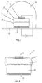
- Figure 4 shows an example of the structure of a conventional light emitting device.
- an AlGaAs chip 10 which comprises an n-type layer 11 and a p-type layer 12 has an n-electrode 13 on the n-type layer side and a p-electrode 14 on the p-type layer side, and the chip 10 is fixed to a base 16 by silver paste and such.
- the chip 10 is sealed entirely with epoxy resin mold 15.
- epoxy resin is hygroscopic and is poor in an effect of moisture prevention. Therefore, under high humidity, moisture in the air penetrates into the epoxy resin mold 15 and reacts with AlGaAs, particularly when an electric current flows in the light emitting device during operation, changing in quality of the surface. As shown in Figure 5, an opaque altered layer 17 is generated on the top surface and the side surfaces of the n-type layer 11. When this opaque altered layer 17 is generated, the light extraction efficiency decreases and hence the brightness of the light emitting device decreases.
- This method utilizes the fact that an aqueous solution containing ammonia and hydrogen peroxide reacts with AlGaAs mixed crystals to form an aluminum oxide coating layer. That is, the AlGaAs chip 10 is immersed in said ammonia-hydrogen peroxide aqueous solution to form a protective layer 18 primarily composed of aluminum oxide on the light extracting surface (hereafter referred to as the "upper surface") and the side surfaces so that the AlGaAs chip 10 is protected from the penetrating moisture.
- the thickness of this protective layer 18 is preferably 100 nm or more.
- Japanese unexamined patent publication (Tokkai) Hei 4-216683 proposes a method in which an AlGaAs chip is immersed in an aqueous solution containing 0.3-0.6 wt% of ammonia and 25-35 wt% of hydrogen peroxide to form a protective layer on said chip surface.
- the upper surface (the surface on the side of the n-type layer 11 in Figure 4) or the surface which is to be fixed to a base (the surface on the side of the p-type layer 12 in Figure 4, hereafter referred to as the "lower surface") is adhered to an adhesive sheet, and the AlGaAs chip 10, together with the adhesive sheet, is immersed in said ammonia-hydrogen peroxide aqueous solution.
- the protective layer 18 is not formed or has difficulty forming on the surface which is adhered to the adhesive sheet, and the chip's lower surface does not need the protective layer 18 since it will be fixed to the base 16.
- the AlGaAs chip 10 is immersed in an ammonia-hydrogen peroxide aqueous solution, and particularly the chip 10 is immersed in an ammonia-hydrogen peroxide aqueous solution with the lower chip surface (the surface which is to be fixed to the base, i.e. the surface on the side of the p-type layer 12 in Figure 4) adhered to an adhesive sheet.
- the lower chip surface the surface which is to be fixed to the base, i.e. the surface on the side of the p-type layer 12 in Figure 4
- the generation rate of the protective layer 18 on the side of the p-type layer 12 became smaller relative to the rate on the side of the n-type layer 11, hence the protective layer 18 on the side of the p-type layer 12 became even thinner.
- the object of this invention is to provide a method of manufacturing a light emitting device which allows formation of a protective layer with a sufficient thickness, 100 nm or more, on the side of the p-type layer, without causing cracks in the coating layer on the side of the n-type layer of the AlGaAs chip, thus preventing a reduction in brightness, even under the condition of high humidity.
- This invention provides a method of manufacturing a light emitting device characterized by the fact that an AlGaAs chip which has an n-type layer(s) and a p-type layer(s) is treated with the following processes to form a protective layer primarily composed of aluminum oxide on the top surface and the side surfaces of the AlGaAs chip:
- the thickness of the formed protective layer composed primarily of aluminum oxide is preferably 100 nm or more.
- This invention begins with a process in which the AlGaAs chip is immersed in an ammonia-hydrogen peroxide aqueous solution containing 0.2-0.6 wt% of ammonia and 25-35 wt% of hydrogen peroxide, so that an aluminum oxide coating layer is formed on the AlGaAs chip surface (the primary process).
- the primary process just as in conventional methods, a thick coating layer is formed on the side of the n-type layer and a thin coating layer is formed on the side of the p-type layer.
- the AlGaAs chip is then dried to harden the coating layer, thus forming a passivated, finer (higher density) and more stable layer (the drying process).
- a process is then performed in which the AlGaAs chip is immersed again in an ammonia-hydrogen peroxide aqueous solution containing 0.2-0.6 wt% of ammonia and 25-35 wt% of hydrogen peroxide, thus forming a thick coating layer, 100 nm or thicker, on both the side of the n-type layer and the side of the p-type layer (the secondary process).
- the layer generation rates decreases on both the side of the n-type layer and the side of the p-type layer.
- the layer generation rate on the side of the n-type layer, onto which a thicker layer has already been formed is relatively small compared with the rate on the side of the p-type layer, hence the newly formed coating layer will be thinner and will not become thick enough to cause cracks.
- a relatively thick coating layer will be newly formed, allowing the formation of a final protective layer with a thickness of 100 nm or more.
- Formation of a layer with a more uniform thickness is possible by the following method: first immersing the AlGaAs chip in the ammonia-hydrogen peroxide aqueous solution with its lower surface (the surface which is to be fixed to the base) adhered to an adhesive sheet; taking out the AlGaAs chip from said aqueous solution and drying it; switching the surface of said AlGaAs chip which is adhered to the adhesive sheet from the lower surface to the upper surface (the surface on the light extracting side) (sheet transfer); and then immersing the AlGaAs chip in the ammonia-hydrogen peroxide aqueous solution with its upper surface adhered to the adhesive sheet.
- the upper chip surface of the AlGaAs chip is adhered to the adhesive sheet in the primary process and the chip's lower surface is adhered to the adhesive sheet in the second process for layer generation, the upper surface of the AlGaAs chip is contaminated by the adhesive and good layer formation on said chip upper surface may not be possible in the second process.
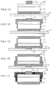
- Figure 1 is a process diagram showing the method of one example of this invention.
- Figure 2 is a process diagram showing the method of another example of this invention.
- Figure 3 is a graph showing results of the high-temperature/ high-humidity reliability testing on light emitting devices prepared with the methods of the examples and light emitting devices prepared with a conventional method.
- Figure 4 is a configuration diagram showing the structure of a light emitting device.
- Figure 5 shows a cross section of an AlGaAs chip on which a clouded layer is generated.
- Figure 6 shows a cross section of an AlGaAs chip on which an ununiform protective layer with large thickness difference is formed.
- Figure 1 is a process diagram showing the method of Example 1.
- parts that are identical to or the equivalent of their counterparts in Figures 4 through 6 are given the same symbols and a description of them is omitted.
- (1) the primary process, (2) the drying process, and (3) the secondary process, shown below, are performed in this order.
- Figure 2 is a process diagram showing the method of Example 2.
- parts that are identical to or the equivalent of their counterparts in Figures 4 through 6 are given the same symbols and a description of them is omitted.
- the primary process, (2) the drying process, and (3) the secondary process, shown below are performed in this order. Characteristic of this example is that it includes the so-called "sheet transfer" of the chip 10.
- Figure 3 is a graph showing the time dependent change in the brightness ratio compared with the initial brightness when high temperature and high humidity testing was carried out for the light emitting devices prepared in the methods of Example 1 and Example 2, as well as a light emitting device prepared with a conventional method.
- the light emitting device of Example 2 showed an even smaller reduction, although not by much, in the brightness ratio compared with the light emitting device of Example 1, indicating a better result.
- this invention allows formation of a fine (high density) and uniform protective layer on the side surfaces of an AlGaAs chip, and therefore a light emitting device equipped with this chip does not sustain a reduction in brightness even under highly humid conditions and is highly reliable over an extended period of time.
Landscapes
- Led Devices (AREA)
Applications Claiming Priority (2)
| Application Number | Priority Date | Filing Date | Title |
|---|---|---|---|
| JP261903/93 | 1993-09-24 | ||
| JP26190393A JP2817590B2 (ja) | 1993-09-24 | 1993-09-24 | 発光素子の製造方法 |
Publications (2)
| Publication Number | Publication Date |
|---|---|
| EP0645829A1 true EP0645829A1 (de) | 1995-03-29 |
| EP0645829B1 EP0645829B1 (de) | 1998-07-22 |
Family
ID=17368360
Family Applications (1)
| Application Number | Title | Priority Date | Filing Date |
|---|---|---|---|
| EP94115044A Expired - Lifetime EP0645829B1 (de) | 1993-09-24 | 1994-09-23 | Verfahren zum Herstellen einer lichtemittierenden Halbleitervorrichtung |
Country Status (4)
| Country | Link |
|---|---|
| US (1) | US5459106A (de) |
| EP (1) | EP0645829B1 (de) |
| JP (1) | JP2817590B2 (de) |
| DE (1) | DE69411836T2 (de) |
Cited By (3)
| Publication number | Priority date | Publication date | Assignee | Title |
|---|---|---|---|---|
| EP1569281A3 (de) * | 2004-02-27 | 2011-03-23 | OSRAM Opto Semiconductors GmbH | Strahlungsemittierender Halbleiterchip and Verfahren zur Herstellung eines solchen Halbleiterchips |
| CN102610708A (zh) * | 2011-01-19 | 2012-07-25 | 鼎元光电科技股份有限公司 | 发光二极管的制法 |
| DE10261675B4 (de) * | 2002-12-31 | 2013-08-14 | Osram Opto Semiconductors Gmbh | Optoelektronisches Bauelement mit strahlungsdurchlässiger elektrischer Kontaktschicht |
Families Citing this family (8)
| Publication number | Priority date | Publication date | Assignee | Title |
|---|---|---|---|---|
| US6013540A (en) * | 1998-05-01 | 2000-01-11 | Lucent Technologies, Inc. | Laser diode with substrate-side protection |
| US6201264B1 (en) * | 1999-01-14 | 2001-03-13 | Lumileds Lighting, U.S., Llc | Advanced semiconductor devices fabricated with passivated high aluminum content III-V materials |
| JP2005026688A (ja) * | 2003-06-30 | 2005-01-27 | Osram Opto Semiconductors Gmbh | 放射放出半導体チップ、該半導体チップの作製方法および該半導体チップの明るさの調整設定方法 |
| CN100460942C (zh) * | 2004-06-02 | 2009-02-11 | 中芯国际集成电路制造(上海)有限公司 | 硅上液晶器件及其制造方法 |
| JP5244703B2 (ja) | 2009-05-22 | 2013-07-24 | 昭和電工株式会社 | 発光ダイオード及び発光ダイオードランプ、並びに照明装置 |
| US20200098698A1 (en) * | 2018-09-26 | 2020-03-26 | Intel Corporation | Novel wafer level chip scale package (wlcsp), flip-chip chip scale package (fccsp), and fan out shielding concepts |
| CN112259450A (zh) * | 2020-09-18 | 2021-01-22 | 厦门市三安集成电路有限公司 | 一种分段式蚀刻方法 |
| CN114188458B (zh) * | 2021-12-02 | 2023-05-02 | 重庆康佳光电技术研究院有限公司 | 一种发光二极管的制作方法及发光二极管 |
Citations (1)
| Publication number | Priority date | Publication date | Assignee | Title |
|---|---|---|---|---|
| JPH04216683A (ja) * | 1990-12-17 | 1992-08-06 | Shin Etsu Handotai Co Ltd | 発光素子の製造方法 |
Family Cites Families (8)
| Publication number | Priority date | Publication date | Assignee | Title |
|---|---|---|---|---|
| US3914465A (en) * | 1972-09-25 | 1975-10-21 | Bell Telephone Labor Inc | Surface passivation of GaAs junction laser devices |
| JPS4995591A (de) * | 1973-01-12 | 1974-09-10 | ||
| JPS4995592A (de) * | 1973-01-12 | 1974-09-10 | ||
| JPS5816535A (ja) * | 1981-07-23 | 1983-01-31 | Matsushita Electric Ind Co Ltd | 半導体装置およびその製造方法 |
| FI64878C (fi) * | 1982-05-10 | 1984-01-10 | Lohja Ab Oy | Kombinationsfilm foer isynnerhet tunnfilmelektroluminensstrukturer |
| JPS6413740A (en) * | 1987-03-23 | 1989-01-18 | Toshiba Corp | Formation of wiring layer in semiconductor device |
| US5262360A (en) * | 1990-12-31 | 1993-11-16 | The Board Of Trustees Of The University Of Illinois | AlGaAs native oxide |
| JPH05129662A (ja) * | 1991-10-31 | 1993-05-25 | Iwasaki Electric Co Ltd | 発光ダイオードランプの製造方法 |
-
1993
- 1993-09-24 JP JP26190393A patent/JP2817590B2/ja not_active Expired - Lifetime
-
1994
- 1994-09-22 US US08/310,088 patent/US5459106A/en not_active Expired - Fee Related
- 1994-09-23 EP EP94115044A patent/EP0645829B1/de not_active Expired - Lifetime
- 1994-09-23 DE DE69411836T patent/DE69411836T2/de not_active Expired - Fee Related
Patent Citations (1)
| Publication number | Priority date | Publication date | Assignee | Title |
|---|---|---|---|---|
| JPH04216683A (ja) * | 1990-12-17 | 1992-08-06 | Shin Etsu Handotai Co Ltd | 発光素子の製造方法 |
Cited By (4)
| Publication number | Priority date | Publication date | Assignee | Title |
|---|---|---|---|---|
| DE10261675B4 (de) * | 2002-12-31 | 2013-08-14 | Osram Opto Semiconductors Gmbh | Optoelektronisches Bauelement mit strahlungsdurchlässiger elektrischer Kontaktschicht |
| EP1569281A3 (de) * | 2004-02-27 | 2011-03-23 | OSRAM Opto Semiconductors GmbH | Strahlungsemittierender Halbleiterchip and Verfahren zur Herstellung eines solchen Halbleiterchips |
| CN102610708A (zh) * | 2011-01-19 | 2012-07-25 | 鼎元光电科技股份有限公司 | 发光二极管的制法 |
| CN102610708B (zh) * | 2011-01-19 | 2014-09-03 | 鼎元光电科技股份有限公司 | 发光二极管的制法 |
Also Published As
| Publication number | Publication date |
|---|---|
| JPH0794777A (ja) | 1995-04-07 |
| EP0645829B1 (de) | 1998-07-22 |
| DE69411836D1 (de) | 1998-08-27 |
| DE69411836T2 (de) | 1999-03-18 |
| JP2817590B2 (ja) | 1998-10-30 |
| US5459106A (en) | 1995-10-17 |
Similar Documents
| Publication | Publication Date | Title |
|---|---|---|
| EP0645829B1 (de) | Verfahren zum Herstellen einer lichtemittierenden Halbleitervorrichtung | |
| US4205099A (en) | Method for making terminal bumps on semiconductor wafers | |
| US3844029A (en) | High power double-slug diode package | |
| US3936855A (en) | Light-emitting diode fabrication process | |
| US4946518A (en) | Method for improving the adhesion of a plastic encapsulant to copper containing leadframes | |
| CA1205578A (en) | Method for manufacturing an integrated circuit device | |
| EP0365107A3 (de) | Verfahren zur Herstellung von vertikalleitenden Halbleiterbauelementen | |
| US20060110855A1 (en) | Leadframe with enhanced encapsulation adhesion | |
| US9640466B1 (en) | Packaged semiconductor device with a lead frame and method for forming | |
| CN104576309B (zh) | 从多芯片封装结构中获取底层芯片的方法 | |
| US5901436A (en) | Method of manufacturing lead frame | |
| US7691679B2 (en) | Pre-plated leadframe having enhanced encapsulation adhesion | |
| US3324015A (en) | Electroplating process for semiconductor devices | |
| US3876461A (en) | Semiconductor process | |
| US3817798A (en) | Method of forming integrated semiconductor devices with iii-v compounds | |
| US3926695A (en) | Etched silicon washed emitter process | |
| JP2559536B2 (ja) | 発光素子の製造方法 | |
| JPH11111908A (ja) | リード形成材及びその樹脂密着性向上表面処理方法 | |
| JPH0817788A (ja) | 半導体素子の製造方法 | |
| US4145262A (en) | Method of manufacturing a semiconductor device and semiconductor device manufactured according to the method | |
| JPS5571038A (en) | Splitting method for semiconductor wafer | |
| JPS5629355A (en) | Manufacture of resin-sealed semiconductor device | |
| JPS6428943A (en) | Package for semiconductor integrated circuit | |
| JPS6394640A (ja) | 半導体素子の製造方法 | |
| KR0156105B1 (ko) | 반도체 칩과 리드프레임의 연결 방법 |
Legal Events
| Date | Code | Title | Description |
|---|---|---|---|
| PUAI | Public reference made under article 153(3) epc to a published international application that has entered the european phase |
Free format text: ORIGINAL CODE: 0009012 |
|
| AK | Designated contracting states |
Kind code of ref document: A1 Designated state(s): DE FR GB |
|
| 17P | Request for examination filed |
Effective date: 19950503 |
|
| 17Q | First examination report despatched |
Effective date: 19960718 |
|
| GRAG | Despatch of communication of intention to grant |
Free format text: ORIGINAL CODE: EPIDOS AGRA |
|
| GRAG | Despatch of communication of intention to grant |
Free format text: ORIGINAL CODE: EPIDOS AGRA |
|
| GRAH | Despatch of communication of intention to grant a patent |
Free format text: ORIGINAL CODE: EPIDOS IGRA |
|
| GRAH | Despatch of communication of intention to grant a patent |
Free format text: ORIGINAL CODE: EPIDOS IGRA |
|
| GRAA | (expected) grant |
Free format text: ORIGINAL CODE: 0009210 |
|
| AK | Designated contracting states |
Kind code of ref document: B1 Designated state(s): DE FR GB |
|
| PGFP | Annual fee paid to national office [announced via postgrant information from national office to epo] |
Ref country code: FR Payment date: 19980818 Year of fee payment: 5 |
|
| REF | Corresponds to: |
Ref document number: 69411836 Country of ref document: DE Date of ref document: 19980827 |
|
| PGFP | Annual fee paid to national office [announced via postgrant information from national office to epo] |
Ref country code: GB Payment date: 19980916 Year of fee payment: 5 |
|
| PGFP | Annual fee paid to national office [announced via postgrant information from national office to epo] |
Ref country code: DE Payment date: 19980923 Year of fee payment: 5 |
|
| ET | Fr: translation filed | ||
| PLBE | No opposition filed within time limit |
Free format text: ORIGINAL CODE: 0009261 |
|
| STAA | Information on the status of an ep patent application or granted ep patent |
Free format text: STATUS: NO OPPOSITION FILED WITHIN TIME LIMIT |
|
| 26N | No opposition filed | ||
| PG25 | Lapsed in a contracting state [announced via postgrant information from national office to epo] |
Ref country code: GB Free format text: LAPSE BECAUSE OF NON-PAYMENT OF DUE FEES Effective date: 19990923 |
|
| GBPC | Gb: european patent ceased through non-payment of renewal fee |
Effective date: 19990923 |
|
| PG25 | Lapsed in a contracting state [announced via postgrant information from national office to epo] |
Ref country code: FR Free format text: LAPSE BECAUSE OF NON-PAYMENT OF DUE FEES Effective date: 20000531 |
|
| PG25 | Lapsed in a contracting state [announced via postgrant information from national office to epo] |
Ref country code: DE Free format text: LAPSE BECAUSE OF NON-PAYMENT OF DUE FEES Effective date: 20000701 |
|
| REG | Reference to a national code |
Ref country code: FR Ref legal event code: ST |