EP0635879A2 - Silizium-Halbleiterplättchen und Verfahren zur Herstellung - Google Patents
Silizium-Halbleiterplättchen und Verfahren zur Herstellung Download PDFInfo
- Publication number
- EP0635879A2 EP0635879A2 EP94111305A EP94111305A EP0635879A2 EP 0635879 A2 EP0635879 A2 EP 0635879A2 EP 94111305 A EP94111305 A EP 94111305A EP 94111305 A EP94111305 A EP 94111305A EP 0635879 A2 EP0635879 A2 EP 0635879A2
- Authority
- EP
- European Patent Office
- Prior art keywords
- silicon wafer
- semiconductor silicon
- semiconductor
- heat treatment
- polycrystal
- Prior art date
- Legal status (The legal status is an assumption and is not a legal conclusion. Google has not performed a legal analysis and makes no representation as to the accuracy of the status listed.)
- Granted
Links
Images


Classifications
-
- C—CHEMISTRY; METALLURGY
- C30—CRYSTAL GROWTH
- C30B—SINGLE-CRYSTAL GROWTH; UNIDIRECTIONAL SOLIDIFICATION OF EUTECTIC MATERIAL OR UNIDIRECTIONAL DEMIXING OF EUTECTOID MATERIAL; REFINING BY ZONE-MELTING OF MATERIAL; PRODUCTION OF A HOMOGENEOUS POLYCRYSTALLINE MATERIAL WITH DEFINED STRUCTURE; SINGLE CRYSTALS OR HOMOGENEOUS POLYCRYSTALLINE MATERIAL WITH DEFINED STRUCTURE; AFTER-TREATMENT OF SINGLE CRYSTALS OR A HOMOGENEOUS POLYCRYSTALLINE MATERIAL WITH DEFINED STRUCTURE; APPARATUS THEREFOR
- C30B29/00—Single crystals or homogeneous polycrystalline material with defined structure characterised by the material or by their shape
- C30B29/02—Elements
- C30B29/06—Silicon
-
- H—ELECTRICITY
- H10—SEMICONDUCTOR DEVICES; ELECTRIC SOLID-STATE DEVICES NOT OTHERWISE PROVIDED FOR
- H10P—GENERIC PROCESSES OR APPARATUS FOR THE MANUFACTURE OR TREATMENT OF DEVICES COVERED BY CLASS H10
- H10P36/00—Gettering within semiconductor bodies
-
- C—CHEMISTRY; METALLURGY
- C30—CRYSTAL GROWTH
- C30B—SINGLE-CRYSTAL GROWTH; UNIDIRECTIONAL SOLIDIFICATION OF EUTECTIC MATERIAL OR UNIDIRECTIONAL DEMIXING OF EUTECTOID MATERIAL; REFINING BY ZONE-MELTING OF MATERIAL; PRODUCTION OF A HOMOGENEOUS POLYCRYSTALLINE MATERIAL WITH DEFINED STRUCTURE; SINGLE CRYSTALS OR HOMOGENEOUS POLYCRYSTALLINE MATERIAL WITH DEFINED STRUCTURE; AFTER-TREATMENT OF SINGLE CRYSTALS OR A HOMOGENEOUS POLYCRYSTALLINE MATERIAL WITH DEFINED STRUCTURE; APPARATUS THEREFOR
- C30B15/00—Single-crystal growth by pulling from a melt, e.g. Czochralski method
-
- C—CHEMISTRY; METALLURGY
- C30—CRYSTAL GROWTH
- C30B—SINGLE-CRYSTAL GROWTH; UNIDIRECTIONAL SOLIDIFICATION OF EUTECTIC MATERIAL OR UNIDIRECTIONAL DEMIXING OF EUTECTOID MATERIAL; REFINING BY ZONE-MELTING OF MATERIAL; PRODUCTION OF A HOMOGENEOUS POLYCRYSTALLINE MATERIAL WITH DEFINED STRUCTURE; SINGLE CRYSTALS OR HOMOGENEOUS POLYCRYSTALLINE MATERIAL WITH DEFINED STRUCTURE; AFTER-TREATMENT OF SINGLE CRYSTALS OR A HOMOGENEOUS POLYCRYSTALLINE MATERIAL WITH DEFINED STRUCTURE; APPARATUS THEREFOR
- C30B33/00—After-treatment of single crystals or homogeneous polycrystalline material with defined structure
-
- H—ELECTRICITY
- H10—SEMICONDUCTOR DEVICES; ELECTRIC SOLID-STATE DEVICES NOT OTHERWISE PROVIDED FOR
- H10D—INORGANIC ELECTRIC SEMICONDUCTOR DEVICES
- H10D18/00—Thyristors
- H10D18/01—Manufacture or treatment
- H10D18/031—Manufacture or treatment of lateral or planar thyristors
-
- H—ELECTRICITY
- H10—SEMICONDUCTOR DEVICES; ELECTRIC SOLID-STATE DEVICES NOT OTHERWISE PROVIDED FOR
- H10P—GENERIC PROCESSES OR APPARATUS FOR THE MANUFACTURE OR TREATMENT OF DEVICES COVERED BY CLASS H10
- H10P36/00—Gettering within semiconductor bodies
- H10P36/03—Gettering within semiconductor bodies within silicon bodies
-
- H—ELECTRICITY
- H10—SEMICONDUCTOR DEVICES; ELECTRIC SOLID-STATE DEVICES NOT OTHERWISE PROVIDED FOR
- H10P—GENERIC PROCESSES OR APPARATUS FOR THE MANUFACTURE OR TREATMENT OF DEVICES COVERED BY CLASS H10
- H10P36/00—Gettering within semiconductor bodies
- H10P36/20—Intrinsic gettering, i.e. thermally inducing defects by using oxygen present in the silicon body
-
- Y—GENERAL TAGGING OF NEW TECHNOLOGICAL DEVELOPMENTS; GENERAL TAGGING OF CROSS-SECTIONAL TECHNOLOGIES SPANNING OVER SEVERAL SECTIONS OF THE IPC; TECHNICAL SUBJECTS COVERED BY FORMER USPC CROSS-REFERENCE ART COLLECTIONS [XRACs] AND DIGESTS
- Y10—TECHNICAL SUBJECTS COVERED BY FORMER USPC
- Y10S—TECHNICAL SUBJECTS COVERED BY FORMER USPC CROSS-REFERENCE ART COLLECTIONS [XRACs] AND DIGESTS
- Y10S148/00—Metal treatment
- Y10S148/06—Gettering
-
- Y—GENERAL TAGGING OF NEW TECHNOLOGICAL DEVELOPMENTS; GENERAL TAGGING OF CROSS-SECTIONAL TECHNOLOGIES SPANNING OVER SEVERAL SECTIONS OF THE IPC; TECHNICAL SUBJECTS COVERED BY FORMER USPC CROSS-REFERENCE ART COLLECTIONS [XRACs] AND DIGESTS
- Y10—TECHNICAL SUBJECTS COVERED BY FORMER USPC
- Y10S—TECHNICAL SUBJECTS COVERED BY FORMER USPC CROSS-REFERENCE ART COLLECTIONS [XRACs] AND DIGESTS
- Y10S148/00—Metal treatment
- Y10S148/061—Gettering-armorphous layers
Definitions
- the present invention relates to a process for producing a semiconductor silicon wafer.
- the present invention relates to a semiconductor silicon wafer having not only a high gettering ability but also a denuded zone on the top side (surface) thereof, and to a process for producing it.
- Semiconductor silicon wafers are obtained by slicing a silicon ingot into wafers, and then various heat treatments are effected on the thus obtained semiconductor silicon wafers in the device processes.
- gettering techniques are used to let metal contaminations, which were introduced into a semiconductor silicon wafer in the device processes, be captured in a region other than an element active region.
- the gettering techniques are classified into two large groups.
- IG intrinsic gettering
- EG extrinsic gettering
- the most generally used EG is a sand-blasting method, in which fine scars having a size of about 1 ⁇ m or less are formed by bombarding the back side of the semiconductor silicon wafer with fine silicon particles. Then, the semiconductor silicon wafer thus obtained is oxidized to cause oxidation-induced stacking faults (OSF) or dislocation from the scars, so that the back side of the semiconductor silicon wafer becomes metal gettering sites (Fig. 12B). However, silicon (Si) could be peeled off in a scar portion so as to produce fine dust.
- OSF oxidation-induced stacking faults
- Fig. 12B metal gettering sites
- a recent method drawing attention as EG with high gettering ability is a process for producing a semiconductor silicon wafer having polycrystal silicon on the back side.
- This is a process in which polycrystal silicon is deposited by the vapor growth method (CVD) on the back side of a silicon wafer sliced off from a silicon ingot in the form of a wafer.
- CVD vapor growth method
- oxygen precipitates can be induced by the gettering effect in the polycrystal grain boundaries and by the heat treatments in the device processes, whereby both effects of EG and IG can be expected (Fig. 12C).
- the silicon wafer having back side polycrystal silicon shows, however, that the density of oxygen precipitates is higher in the vicinity of the top side.
- Such oxygen precipitates in the vicinity of the top side become recombination centers of carriers, which in turn cause degradation of device characteristics, or crystal defects.
- the silicon wafer when the silicon wafer is subjected to a heat treatment at a high temperature in a reducing atmosphere for forming a denuded zone on the top side, employing the conventional extrinsic gettering method for forming a polycrystal silicon film on the back side of a silicon wafer, the back side polycrystal silicon film is recrystallized, whereby the thickness of the polycrystal silicon film might be considerably reduced so as to considerably lower the gettering ability.
- An object of the present invention is to provide a semiconductor silicon wafer which has a high gettering ability, which can form a denuded zone on the top side and which can fully suppress a decrease of polycrystal silicon film during heat treatments at high temperature, and further to provide a process for producing it.
- the present invention provides, as in Claim 1, a process for producing a semiconductor silicon wafer, comprising a step of forming a polycrystal silicon depositing film on one side of a silicon wafer and a subsequent step of subjecting the silicon wafer to a heat treatment in an inert gas, a reducing gas or a mixture thereof.
- the present invention provides, as in Claim 3, a process for producing a semiconductor silicon wafer, comprising a step of subjecting a silicon wafer to a heat treatment in an inert gas, a reducing gas or a mixture thereof, and a subsequent step of forming a polycrystal silicon depositing film on one side of the silicon wafer.
- the present invention provides, as in Claim 7, a process for producing a semiconductor silicon wafer, comprising a step of forming an oxide film having the thickness in the range of about 1 nm-3 nm on one side of a silicon wafer, a step of forming a polycrystal silicon depositing film on the oxide film thus formed and a step of subjecting the silicon wafer to a heat treatment in an inert gas, a reducing gas or a mixture thereof.
- the polycrystal silicon film is doped with at least one of boron, arsenide or phosphorus.
- the above heat treatment is performed at a temperature of at least 1100 °C for 10 minutes and that the thickness of the polycrystal silicon film remains in the range of about 0.5 ⁇ m - 2.5 ⁇ m after the above heat treatment.
- the present invention provides, as in Claim 12, a semiconductor silicon wafer having an oxide film formed in the thickness of about 1 nm-3 nm on one side of the silicon wafer and a polycrystal silicon depositing film formed on the surface of the oxide film.
- the thickness of the polycrystal silicon depositing film is preferably about 0.5 ⁇ m - 2.5 ⁇ m.
- the process for producing a semiconductor silicon wafer includes forming a polycrystal silicon depositing film on one side of silicon wafer and discharging oxygen from the other side, so that oxygen precipitates are produced by the heat treatments in the device processes, whereby the gettering effect can be improved and a denuded zone can be formed on the other side.
- a polycrystal silicon film is deposited on the back side of the silicon wafer after an oxide film is formed in the thickness of 1 nm-3 nm on the back side of the silicon wafer, and the recrystallization of the polycrystal silicon can be suppressed by the oxide film in the subsequent heat treatments. Accordingly, a high gettering ability can be maintained throughout the semiconductor fabricating processes.
- Figs. 1A to 8 are drawings to show the first embodiment of the process for producing semiconductor silicon wafers according to the present invention.
- Fig. 1A shows a flow chart of the process according to the first embodiment of the present invention.
- the silicon ingot 10 is cut into wafers to obtain silicon wafers 11 (slicing). Then, the edges of each silicon wafer 11 are made round (beveling) and the silicon wafer 11 is subjected to lapping to make its thickness close to the standard thickness, followed by etching to remove crushed layers by the lapping.
- a polycrystal silicon film 12 is deposited in the thickness of 1 ⁇ m on the top and back sides of silicon wafer 11 by the CVD method. Then, only the top side is subjected to mirror polishing so as to remove the polycrystal silicon film 12 from the top side. Finally, oxygen in the vicinity of the top side is discharged to the outside by a heat treatment at 1200 °C for 1 hour in a H2 atmosphere.
- Fig. 2 shows an oxygen concentration distribution in the vicinity of the top side along the thickness of a semiconductor silicon wafer 15 thus obtained.
- the oxygen concentration in the vicinity of the top side (0-20 ⁇ m) is extremely reduced by the heat treatment in the H2 reducing atmosphere, whereby a denuded zone can be formed near the top side of the semiconductor silicon wafer 15.
- the oxygen concentration after the heat treatment is shown by a solid line and the oxygen concentration before the heat treatment by a dashed line.
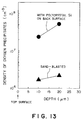
- Measurement was conducted such that the semiconductor silicon wafer 15 was subjected to the CMOS heating treatments and that oxygen precipitates formed on the top side were measured. The results thus obtained are shown in Fig. 3. It is evident from a comparison between Figs. 3 and 13 that a denuded zone can be provided on the top side by using the process of the present embodiment.
- FIG. 1B Another embodiment of the present invention is shown in Fig. 1B.
- a silicon wafer 11 is subjected to a heat treatment to outwardly discharge oxygen from the vicinity of the top and back sides of silicon wafer 11.
- polycrystal silicon 12 is deposited in the thickness of 1.5 ⁇ m on the top and back sides of silicon wafer 11 by the CVD method, and only the top side is mirror-polished.
- the heat treatment is conducted at 1170 °C for 4 hours in an Ar inert gas atmosphere. Measurement was conducted such that the semiconductor silicon wafer thus obtained was subjected to the CMOS heat treatments and that oxygen precipitates formed on the top side were measured. The measurement results are shown in Fig. 4.
- the process as shown in Fig. 1A may be modified such that after depositing the polycrystal silicon 12, the heat treatment is performed at 1200 °C for 2 hours in a He atmosphere instead of that in the H2 atmosphere. Further, replacing the H2 atmosphere, the heat treatment may be conducted in a CO atmosphere at 1150 °C for 30 minutes. Measurement was conducted such that semiconductor silicon wafers 15 obtained by the above heat treatments were subjected to the CMOS heat treatments and that top side oxygen precipitates were measured. The measurement results are shown in Figs. 5 and 6.
- the above processes showed examples in which the heat treatment was performed in the reducing atmosphere or in the inert atmosphere to discharge oxygen from the silicon wafer 11.
- the heat treatment may be performed in an atmosphere of a mixture of a reducing gas and an inert gas.
- CMOS heat treatments were performed for four types of semiconductor silicon wafers, i.e., a semiconductor silicon wafer obtained by the present invention, a conventional semiconductor silicon wafer having polycrystal silicon, a conventional semiconductor silicon wafer subjected to a heat treatment at a high temperature in a reducing atmosphere (1200 °C, H2, 1 hour) and a conventional semiconductor silicon wafer subjected to the sand-blasting treatment, and a distribution of the density of oxygen precipitates in the thickness direction was measured.
- the four types of semiconductor silicon wafers had substrate oxygen concentration of 13 ⁇ 1017 (cm ⁇ 3). The results are shown in Fig. 8.
- oxygen precipitates are formed in the semiconductor silicon wafer which was subjected to the sand-blasting treatment, because of the low substrate oxygen concentration.
- oxygen precipitates are formed in an amount 2-order higher as compared with the semiconductor silicon wafer subjected to the sand-blasting treatment.
- oxygen precipitates are formed in an amount about one-order higher than that of the semiconductor having the polycrystal silicon and that of the semiconductor silicon wafer subjected to the high heat treatment in the reducing atmosphere, thus showing that the semiconductor silicon wafer of the present invention has a higher gettering ability.
- Fig. 7 is a drawing to show frequencies for withstand-voltage-acceptable percentage (C+), withstand-voltage-defective percentage (B-) and intermediate percentage (B+).
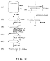
- Figs. 9 and 10 are drawings to show the modifications of the first embodiment of the present invention.
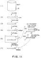
- a conventionally well-known process for producing semiconductor silicon wafers is shown in Fig. 11.
- a silicon ingot 10 is formed by the Cz method (pulling method).
- the silicon ingot 10 is sliced to obtain silicon wafers 11.
- the slicing thickness is about 1 mm.
- the edges of each wafer are made round (bevel formation).
- the thickness of the silicon wafer 11 is made as close as the standard thickness (625 ⁇ m) by lapping.
- Crashed layers by the lapping are removed by etching and (7) mirror-polishing is finally performed for finishing only on one side (top side).
- a donor killer heat treatment is performed at 650 °C after (4) the lapping step or (5) the etching step in order to eliminate thermal donors due to oxygen.
- a sand-blasting treatment or (6a) a polycrystal silicon depositing treatment is conducted after the etching step (5), followed by (7) the last step of mirror-polishing for finishing.
- a manufacturing process of the present invention is described with reference to Fig. 9.
- a silicon ingot 10 is formed by the Cz method, and then (2) the silicon ingot 10 is sliced into wafers to obtain silicon wafers 11.
- the slicing thickness of silicon wafers 11 is about 1 mm.
- a polycrystal silicon depositing film 12 is formed on one side of silicon wafer 11 in the thickness of 1 ⁇ m by the CVD method.
- the polycrystal silicon depositing treatment is conducted in the temperature range of from 620 °C to 650 °C, so that thermal donors in the silicon wafer 11 are annihilated during this depositing treatment, which obviates a separate donor killer treatment.
- (6 b ) oxygen precipitates are preliminarily formed in the polycrystal silicon depositing film by a heat treatment at 1000 °C for 10 hours.
- crushed layers produced by the lapping are removed and (7) mirror-polishing is performed for finishing, whereby a semiconductor silicon wafer 15 is obtained.
- FIG. 10 A manufacturing process as shown in Fig. 10 is the same as that shown in Fig. 9 except that (6 a ) a polycrystal silicon depositing film is formed on one side of silicon wafer 11 after (2) the step of slicing the silicon ingot 10 and (3) the step of beveling formation.
- the polycrystal silicon depositing treatment is conducted at 630 °C and the thickness of the depositing film is 0.8 ⁇ m. Further, the heat treatment for preliminarily forming oxygen precipitates in the polycrystal silicon depositing film 12 is conducted at 950 °C for 8 hours.
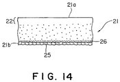
- a semiconductor silicon wafer 21 as shown in Fig. 14 has an oxygen content of about 13 ⁇ 1017 (cm ⁇ 3), which is used in the present embodiment.
- the silicon wafer 21 is treated with a chemical to form an oxide film 26.
- This chemical treatment is performed at 70 °C for 20 minutes using a chemical SH (H2O2/H2SO4), to form the oxide film 26 in the thickness of 2 nm.
- the thickness 2 nm of oxide film 26 is measured by XPS (X-ray photoelectron spectroscopy).
- diluted HF HF:H2O
- SC2 H2O2/HCl/H2O
- NC2 choline/H2O2/H2O
- SH X-ray photoelectron spectroscopy
- an undoped polycrystal silicon film 25 is deposited in the thickness of 1 ⁇ m - 2 ⁇ m by the vapor growth (CVD) method on the back side 21b of the silicon wafer 21 having the oxide film 26 formed thereon.
- CVD vapor growth
- the silicon wafer 21 is subjected to a high-temperature heat treatment at a temperature of at least 1100 °C for 10 minutes in an atmosphere of hydrogen as the reducing gas.
- a high-temperature heat treatment an inert gas such as Ar, He, Xe, Kr, Ne, etc., or a mixture of an inert gas as listed and a reducing gas may be used instead of the reducing gas.
- the silicon wafer 21 thus obtained has a surface denuded zone 22 formed on the top side 21a by the extrinsic gettering effect in the polycrystal grain boundaries of the polycrystal silicon layer 25 deposited on the silicon wafer back side 21b and by the intrinsic gettering effect in the high-temperature heat treatment. Further, the polycrystal silicon film 25 can maintain a sufficient thickness even though subjected to the subsequent high-temperature heat treatment, because recrystallization is suppressed by the existence of the oxide film 26.
- the oxide film 26 serves to suppress recrystallization of the polycrystal silicon film 25.
- the two types of semiconductor silicon wafers of the present invention were those obtained by forming an oxide film in the thickness of 2 nm by the same chemical treatment as above and by depositing a polycrystal silicon film on the oxide film by the vapor growth method in the thickness of 1 ⁇ m or 2 ⁇ m, respectively.
- the two types of conventional semiconductor silicon wafers were those obtained by depositing a polycrystal silicon film by the vapor growth method in the thickness of 1 ⁇ m or 2 ⁇ m, respectively, without forming an oxide film.
- the two types of semiconductor silicon wafers of the present invention and the two types of conventional semiconductor silicon wafers were subjected to a high-temperature heat treatment.
- the high-temperature heat treatment was performed in a hydrogen atmosphere at 1200 °C while a treating time was changed as 0, 0.5 hour, 1 hour, 2 hours, 3 hours and 4 hours.
- the optimum thickness of the oxide film 6 is in the range of about 1 nm to about 3 nm.
- oxide films having the thickness of 0.1 nm, 0.5 nm, 1 nm or 3 nm were formed on four semiconductor silicon wafers using four types of chemicals, i.e., diluted HF(HF:H2O), SC2(H2O2/HCl/H2O), NC2(choline/H2O2/H2O) and SH(H2O2/H2SO4), respectively.
- diluted HF(HF:H2O) diluted HF(HF:H2O)
- SC2(H2O2/HCl/H2O) SC2(H2O2/HCl/H2O)
- NC2(choline/H2O2/H2O) were formed on four semiconductor silicon wafers using four types of chemicals, respectively.
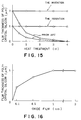
- Fig. 16 The experimental results are shown in Fig. 16, in which the abscissa represents the thickness of oxide film and the ordinate the thickness of polycrystal silicon film. It is clear from the graph that the recrystallization of polycrystal silicon film by the high-temperature heat treatment can be fully suppressed by setting the thickness of oxide film within the range of about 1 nm-3 nm. However, if the thickness of oxide film becomes far larger than about 3 nm, metal impurities are blocked by the oxide film to stop diffusing into the polycrystal silicon film, whereby the gettering effect is considerably reduced.
- a polycrystal silicon film 25 When a polycrystal silicon film 25 is deposited on a wafer as in Fig. 14, it is doped with boron using B2H6 (1019atms/cm3). As the doping material, arsenide or phosphorus may be used instead of boron.
- the depositing thickness of the polycrystal silicon film 25 is preferably so set that when a high-temperature heat treatment is performed at a temperature of at least 1100 °C for 10 or more minutes after the deposition, the polycrystal silicon film 25 remains in the thickness of 0.5 ⁇ m - 2.5 ⁇ m.
- First Example A of the present invention an oxide film was formed in the thickness of 2 nm on the back side of one of the semiconductor silicon wafers, and then a polycrystal silicon film was deposited in the thickness of 1 ⁇ m to obtain a semiconductor silicon A.
- Second Example B of the present invention after forming an oxide film on the back side of another semiconductor silicon wafer in the thickness of 2 nm, a polycrystal silicon film doped with boron (1019atms/cm3) was deposited in the thickness of 1 ⁇ m to obtain a semiconductor silicon B.
- Comparative Example a polycrystal silicon film was deposited in the thickness of 1 ⁇ m without forming an oxide film on the back side of another one of the above semiconductor silicon wafers.
- the two types of semiconductor silicon wafers A and B of the present invention and the conventional semiconductor silicon wafer thus obtained were subjected to a heat treatment at 1200 °C for 1 hour in a hydrogen atmosphere, and then to heat treatments equivalent to the CMOS treatments, e.g., at 1200 °C for 10 hours, at 800 °C for 3 hours and at 1000 °C for 16 hours, and thereafter an oxide film on the top side was peeled off with NH4F. Then, the top side was metal-contaminated with Fe or Ni, and a high temperature heat treatment was conducted at 1000 °C for 16 hours in an oxygen atmosphere to measure faults (OSF) appearing in the top side.
- OSF faults
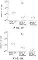
- Figs. 17 and 18 are graphs to show the experimental results of contamination with Ni and Fe, respectively, in which the abscissa shows the two types of semiconductor silicon wafers A and B according to the present invention and the conventional semiconductor silicon wafer, and the ordinate the oxidation-induced stacking faults density (OSF) on the top side of the semiconductor silicon wafers.
- the abscissa shows the two types of semiconductor silicon wafers A and B according to the present invention and the conventional semiconductor silicon wafer
- OSF oxidation-induced stacking faults density
- the conventional semiconductor silicon wafer shows that the polycrystal silicon film is completely removed by the high-temperature heat treatment, the CMOS heat treatments and the peeling-off process of oxide film, so as to lose the gettering ability and produce many surface faults.
- the semiconductor silicon wafers of the present invention show that the recrystallization of the polycrystal silicon film is suppressed by the existence of the oxide film formed on the back side of the silicon wafer and that the polycrystal silicon film fully remains even after the high-temperature heat treatment and the CMOS heat treatments. Therefore, the semiconductor silicon wafers of the invention hold the high gettering ability, so that the oxidation-induced stacking faults density (OSF) on the top side of the semiconductor silicon wafer is remarkably reduced.
- OSF oxidation-induced stacking faults density
- the semiconductor silicon wafer B of the present invention is higher in gettering ability for Fe than the semiconductor silicon wafer A of the present invention, which assures that the boron-doping of polycrystal silicon film enhances the gettering ability for Fe.
- 16M-DRAMs were fabricated using the semiconductor silicon wafers of the present invention as described above and the conventional semiconductor silicon wafers, and it turned out that the semiconductor silicon wafers of the present invention had a 10 % improvement in Y D/S as compared with the conventional semiconductor silicon wafers.
- the intrinsic gettering effect can be improved by producing oxygen precipitates in the polycrystal silicon depositing film formed on one side of the semiconductor silicon wafer when the semiconductor silicon wafer is heat-treated in the device processes, and at the same time, the other side can be made free from faults.
- high-precision semiconductor devices can be obtained.
- a polycrystal silicon film is deposited after an oxide film is formed on the back side of the semiconductor silicon wafer in the thickness of about 1 nm-3 nm, so that the recrystallisation of the polycrystal silicon can be suppressed by the existence of the oxide film in a high-temperature heat treatment after the deposition. Accordingly, the high gettering ability can be maintained throughout the semiconductor fabrication processes, which can fully reduce faults appearing on the top side of the semiconductor silicon wafer due to metal contamination.
Landscapes
- Chemical & Material Sciences (AREA)
- Engineering & Computer Science (AREA)
- Crystallography & Structural Chemistry (AREA)
- Materials Engineering (AREA)
- Metallurgy (AREA)
- Organic Chemistry (AREA)
- Crystals, And After-Treatments Of Crystals (AREA)
- Mechanical Treatment Of Semiconductor (AREA)
- Formation Of Insulating Films (AREA)
Applications Claiming Priority (6)
| Application Number | Priority Date | Filing Date | Title |
|---|---|---|---|
| JP181602/93 | 1993-07-22 | ||
| JP18160293 | 1993-07-22 | ||
| JP18160293 | 1993-07-22 | ||
| JP6128959A JPH0786289A (ja) | 1993-07-22 | 1994-06-10 | 半導体シリコンウェハおよびその製造方法 |
| JP128959/94 | 1994-06-10 | ||
| JP12895994 | 1994-06-10 |
Publications (3)
| Publication Number | Publication Date |
|---|---|
| EP0635879A2 true EP0635879A2 (de) | 1995-01-25 |
| EP0635879A3 EP0635879A3 (de) | 1996-10-23 |
| EP0635879B1 EP0635879B1 (de) | 2002-09-18 |
Family
ID=26464517
Family Applications (1)
| Application Number | Title | Priority Date | Filing Date |
|---|---|---|---|
| EP94111305A Expired - Lifetime EP0635879B1 (de) | 1993-07-22 | 1994-07-20 | Verfahren zur Herstellung von Silizium-Halbleiterplättchen |
Country Status (5)
| Country | Link |
|---|---|
| US (2) | US5534294A (de) |
| EP (1) | EP0635879B1 (de) |
| JP (1) | JPH0786289A (de) |
| KR (1) | KR100232914B1 (de) |
| DE (1) | DE69431385T2 (de) |
Cited By (5)
| Publication number | Priority date | Publication date | Assignee | Title |
|---|---|---|---|---|
| EP0822588A3 (de) * | 1996-08-01 | 1998-02-25 | Siemens Aktiengesellschaft | Dotiertes Siliziumsubstrat |
| EP0973190A3 (de) * | 1998-07-13 | 2000-03-22 | Shin-Etsu Handotai Company Limited | Siliziumplättchen und Verfahren zur deren Herstellung |
| WO2000013209A3 (en) * | 1998-09-02 | 2000-12-21 | Memc Electronic Materials | Thermally annealed silicon wafers having improved intrinsic gettering |
| WO2003052811A1 (fr) * | 2001-12-18 | 2003-06-26 | Komatsu Denshi Kinzoku Kabushiki Kaisha | Plaquette en silicium, et procede d'elaboration |
| EP1624482A3 (de) * | 1998-09-02 | 2007-02-21 | MEMC Electronic Materials, Inc. | Wärmebehandelte Siliziumplättchen mit verbesserter Eigengetterung |
Families Citing this family (48)
| Publication number | Priority date | Publication date | Assignee | Title |
|---|---|---|---|---|
| US5788763A (en) * | 1995-03-09 | 1998-08-04 | Toshiba Ceramics Co., Ltd. | Manufacturing method of a silicon wafer having a controlled BMD concentration |
| JP3134719B2 (ja) * | 1995-06-23 | 2001-02-13 | 信越半導体株式会社 | 半導体ウェーハ研磨用研磨剤及び研磨方法 |
| JP3545131B2 (ja) * | 1996-06-11 | 2004-07-21 | 株式会社半導体エネルギー研究所 | 半導体装置の作製方法 |
| JPH10154713A (ja) * | 1996-11-22 | 1998-06-09 | Shin Etsu Handotai Co Ltd | シリコンウエーハの熱処理方法およびシリコンウエーハ |
| CA2194653A1 (en) * | 1997-01-08 | 1998-07-08 | Junichi Matsushita | Hydrogen heat treatment method of silicon wafers using a high-purity inert substitution gas |
| US5994761A (en) | 1997-02-26 | 1999-11-30 | Memc Electronic Materials Spa | Ideal oxygen precipitating silicon wafers and oxygen out-diffusion-less process therefor |
| US6190631B1 (en) | 1997-04-09 | 2001-02-20 | Memc Electronic Materials, Inc. | Low defect density, ideal oxygen precipitating silicon |
| US6146980A (en) * | 1997-06-04 | 2000-11-14 | United Microelectronics Corp. | Method for manufacturing silicon substrate having gettering capability |
| US6022793A (en) | 1997-10-21 | 2000-02-08 | Seh America, Inc. | Silicon and oxygen ion co-implantation for metallic gettering in epitaxial wafers |
| JP3407629B2 (ja) * | 1997-12-17 | 2003-05-19 | 信越半導体株式会社 | シリコン単結晶ウエーハの熱処理方法ならびにシリコン単結晶ウエーハ |
| US6828690B1 (en) * | 1998-08-05 | 2004-12-07 | Memc Electronic Materials, Inc. | Non-uniform minority carrier lifetime distributions in high performance silicon power devices |
| EP1114454A2 (de) * | 1998-09-02 | 2001-07-11 | MEMC Electronic Materials, Inc. | Silizium auf isolator struktur aus einem einkristallsilizium mit niedriger fehlerdichte |
| US6336968B1 (en) | 1998-09-02 | 2002-01-08 | Memc Electronic Materials, Inc. | Non-oxygen precipitating czochralski silicon wafers |
| US6191010B1 (en) | 1998-09-02 | 2001-02-20 | Memc Electronic Materials, Inc. | Process for preparing an ideal oxygen precipitating silicon wafer |
| US6416836B1 (en) | 1998-10-14 | 2002-07-09 | Memc Electronic Materials, Inc. | Thermally annealed, low defect density single crystal silicon |
| JP3264367B2 (ja) * | 1998-10-14 | 2002-03-11 | 信越半導体株式会社 | サンドブラスト処理剤、それを用いて処理されたウェーハ及びその処理方法 |
| JP2000154070A (ja) * | 1998-11-16 | 2000-06-06 | Suminoe Textile Co Ltd | セラミックス三次元構造体及びその製造方法 |
| JP3719021B2 (ja) | 1998-12-04 | 2005-11-24 | 信越半導体株式会社 | シリコンウエーハの製造方法およびシリコンウエーハ |
| US6284384B1 (en) | 1998-12-09 | 2001-09-04 | Memc Electronic Materials, Inc. | Epitaxial silicon wafer with intrinsic gettering |
| DE19925044B4 (de) * | 1999-05-28 | 2005-07-21 | Siltronic Ag | Halbleiterscheibe mit Kristallgitter-Defekten und Verfahren zur Herstellung derselben |
| US20030051656A1 (en) | 1999-06-14 | 2003-03-20 | Charles Chiun-Chieh Yang | Method for the preparation of an epitaxial silicon wafer with intrinsic gettering |
| JP4748178B2 (ja) * | 1999-07-28 | 2011-08-17 | 株式会社Sumco | 点欠陥の凝集体が存在しないシリコンウェーハの製造方法 |
| US6635587B1 (en) | 1999-09-23 | 2003-10-21 | Memc Electronic Materials, Inc. | Method for producing czochralski silicon free of agglomerated self-interstitial defects |
| US6599815B1 (en) | 2000-06-30 | 2003-07-29 | Memc Electronic Materials, Inc. | Method and apparatus for forming a silicon wafer with a denuded zone |
| EP1295324A1 (de) * | 2000-06-30 | 2003-03-26 | MEMC Electronic Materials, Inc. | Verfahren und vorrichtung zur herstellung eines siliziumwafers mit einer defektfreien zone |
| US6339016B1 (en) | 2000-06-30 | 2002-01-15 | Memc Electronic Materials, Inc. | Method and apparatus for forming an epitaxial silicon wafer with a denuded zone |
| JP4603677B2 (ja) * | 2000-11-09 | 2010-12-22 | 信越半導体株式会社 | アニールウェーハの製造方法及びアニールウェーハ |
| US20110263126A1 (en) | 2000-11-22 | 2011-10-27 | Sumco Corporation | Method for manufacturing a silicon wafer |
| JP2004537161A (ja) * | 2001-04-11 | 2004-12-09 | エムイーエムシー・エレクトロニック・マテリアルズ・インコーポレイテッド | 高抵抗率czシリコンにおけるサーマルドナー生成の制御 |
| TW541581B (en) * | 2001-04-20 | 2003-07-11 | Memc Electronic Materials | Method for the preparation of a semiconductor substrate with a non-uniform distribution of stabilized oxygen precipitates |
| JP4566478B2 (ja) * | 2001-08-09 | 2010-10-20 | シルトロニック・ジャパン株式会社 | シリコン半導体基板およびその製造方法 |
| KR20040029231A (ko) * | 2002-09-25 | 2004-04-06 | 엘지.필립스 엘시디 주식회사 | 형광램프 및 이를 이용한 백라이트 유닛 |
| US6955718B2 (en) * | 2003-07-08 | 2005-10-18 | Memc Electronic Materials, Inc. | Process for preparing a stabilized ideal oxygen precipitating silicon wafer |
| WO2005024908A2 (en) * | 2003-09-05 | 2005-03-17 | Si2 Technologies, Inc. | Laser transfer articles and method of making |
| JP2005093869A (ja) * | 2003-09-19 | 2005-04-07 | Mimasu Semiconductor Industry Co Ltd | シリコンウエーハの再生方法及び再生ウエーハ |
| JP2006294691A (ja) * | 2005-04-06 | 2006-10-26 | Toshiba Corp | 半導体基板及び半導体装置とその製造方法 |
| US8008107B2 (en) * | 2006-12-30 | 2011-08-30 | Calisolar, Inc. | Semiconductor wafer pre-process annealing and gettering method and system for solar cell formation |
| US20090004458A1 (en) * | 2007-06-29 | 2009-01-01 | Memc Electronic Materials, Inc. | Diffusion Control in Heavily Doped Substrates |
| US20090004426A1 (en) * | 2007-06-29 | 2009-01-01 | Memc Electronic Materials, Inc. | Suppression of Oxygen Precipitation in Heavily Doped Single Crystal Silicon Substrates |
| KR100984860B1 (ko) * | 2008-07-10 | 2010-10-04 | 주식회사 하이닉스반도체 | 웨이퍼 가공방법 |
| US7977216B2 (en) | 2008-09-29 | 2011-07-12 | Magnachip Semiconductor, Ltd. | Silicon wafer and fabrication method thereof |
| CN101905877B (zh) * | 2009-06-02 | 2013-01-09 | 清华大学 | 碳纳米管膜的制备方法 |
| KR101381537B1 (ko) * | 2009-06-03 | 2014-04-04 | 글로벌웨어퍼스 재팬 가부시키가이샤 | 실리콘 웨이퍼 및 실리콘 웨이퍼의 열처리 방법 |
| CN101993055B (zh) * | 2009-08-14 | 2013-02-13 | 清华大学 | 碳纳米管膜先驱、碳纳米管膜及其制备方法 |
| WO2012111868A1 (ko) * | 2011-02-16 | 2012-08-23 | 한솔테크닉스(주) | 기판처리시스템 |
| WO2014030450A1 (ja) * | 2012-08-22 | 2014-02-27 | 富士電機株式会社 | 半導体装置の製造方法 |
| CN106463403B (zh) * | 2014-06-02 | 2020-05-05 | 胜高股份有限公司 | 硅晶片及其制造方法 |
| CN114121626B (zh) * | 2020-08-27 | 2025-08-15 | 联华电子股份有限公司 | 一种制作半导体元件的方法 |
Family Cites Families (17)
| Publication number | Priority date | Publication date | Assignee | Title |
|---|---|---|---|---|
| US4053335A (en) * | 1976-04-02 | 1977-10-11 | International Business Machines Corporation | Method of gettering using backside polycrystalline silicon |
| GB2080780B (en) * | 1980-07-18 | 1983-06-29 | Secr Defence | Heat treatment of silicon slices |
| AT380974B (de) * | 1982-04-06 | 1986-08-11 | Shell Austria | Verfahren zum gettern von halbleiterbauelementen |
| US4548654A (en) * | 1983-06-03 | 1985-10-22 | Motorola, Inc. | Surface denuding of silicon wafer |
| US4666532A (en) * | 1984-05-04 | 1987-05-19 | Monsanto Company | Denuding silicon substrates with oxygen and halogen |
| JPS61135128A (ja) * | 1984-12-06 | 1986-06-23 | Toshiba Corp | 半導体装置の製造方法 |
| JPH0648686B2 (ja) * | 1988-03-30 | 1994-06-22 | 新日本製鐵株式会社 | ゲッタリング能力の優れたシリコンウェーハおよびその製造方法 |
| US5189508A (en) * | 1988-03-30 | 1993-02-23 | Nippon Steel Corporation | Silicon wafer excelling in gettering ability and method for production thereof |
| DE3910185C2 (de) * | 1988-03-30 | 1998-09-24 | Nippon Steel Corp | Siliziumplättchen mit hervorragendem Gettervermögen und Verfahren zu dessen Herstellung |
| JPH0247836A (ja) * | 1988-08-10 | 1990-02-16 | Nec Corp | 半導体装置の製造方法 |
| JPH0828353B2 (ja) * | 1988-12-28 | 1996-03-21 | 東芝セラミックス株式会社 | 保管用保護被膜付きシリコンウエハ及びシリコンウエハの保管用保護被膜の形成方法 |
| JP2774855B2 (ja) * | 1990-03-23 | 1998-07-09 | 新日本製鐵株式会社 | ゲッタリング効果増強シリコン基板及びその製造方法 |
| JPH0453140A (ja) * | 1990-06-18 | 1992-02-20 | Fujitsu Ltd | シリコン単結晶ウエハの処理方法 |
| JP3063143B2 (ja) * | 1990-10-29 | 2000-07-12 | 日本電気株式会社 | Si基板の製造方法 |
| JPH04171827A (ja) * | 1990-11-05 | 1992-06-19 | Nec Yamagata Ltd | 半導体装置の製造方法 |
| JP2762183B2 (ja) * | 1991-09-17 | 1998-06-04 | 三菱マテリアル株式会社 | シリコン基板の製造方法 |
| JP3024409B2 (ja) * | 1992-12-25 | 2000-03-21 | 日本電気株式会社 | 半導体装置の製造方法 |
-
1994
- 1994-06-10 JP JP6128959A patent/JPH0786289A/ja active Pending
- 1994-07-19 KR KR1019940017349A patent/KR100232914B1/ko not_active Expired - Fee Related
- 1994-07-20 EP EP94111305A patent/EP0635879B1/de not_active Expired - Lifetime
- 1994-07-20 DE DE69431385T patent/DE69431385T2/de not_active Expired - Fee Related
- 1994-07-22 US US08/279,007 patent/US5534294A/en not_active Expired - Lifetime
-
1995
- 1995-12-29 US US08/580,926 patent/US5738942A/en not_active Expired - Fee Related
Cited By (9)
| Publication number | Priority date | Publication date | Assignee | Title |
|---|---|---|---|---|
| EP0822588A3 (de) * | 1996-08-01 | 1998-02-25 | Siemens Aktiengesellschaft | Dotiertes Siliziumsubstrat |
| EP0973190A3 (de) * | 1998-07-13 | 2000-03-22 | Shin-Etsu Handotai Company Limited | Siliziumplättchen und Verfahren zur deren Herstellung |
| WO2000013209A3 (en) * | 1998-09-02 | 2000-12-21 | Memc Electronic Materials | Thermally annealed silicon wafers having improved intrinsic gettering |
| US6361619B1 (en) | 1998-09-02 | 2002-03-26 | Memc Electronic Materials, Inc. | Thermally annealed wafers having improved internal gettering |
| US6686260B2 (en) | 1998-09-02 | 2004-02-03 | Memc Electronics Materials, Inc. | Process for producing thermally annealed wafers having improved internal gettering |
| EP1624482A3 (de) * | 1998-09-02 | 2007-02-21 | MEMC Electronic Materials, Inc. | Wärmebehandelte Siliziumplättchen mit verbesserter Eigengetterung |
| KR100816696B1 (ko) * | 1998-09-02 | 2008-03-27 | 엠이엠씨 일렉트로닉 머티리얼즈 인코포레이티드 | 개선된 내부 게터링을 갖는 열어닐된 웨이퍼 |
| WO2003052811A1 (fr) * | 2001-12-18 | 2003-06-26 | Komatsu Denshi Kinzoku Kabushiki Kaisha | Plaquette en silicium, et procede d'elaboration |
| JP2003188176A (ja) * | 2001-12-18 | 2003-07-04 | Komatsu Electronic Metals Co Ltd | シリコンウェーハおよびシリコンウェーハの製造方法 |
Also Published As
| Publication number | Publication date |
|---|---|
| US5738942A (en) | 1998-04-14 |
| US5534294A (en) | 1996-07-09 |
| KR950004449A (ko) | 1995-02-18 |
| EP0635879A3 (de) | 1996-10-23 |
| DE69431385D1 (de) | 2002-10-24 |
| JPH0786289A (ja) | 1995-03-31 |
| DE69431385T2 (de) | 2003-05-15 |
| KR100232914B1 (ko) | 1999-12-01 |
| EP0635879B1 (de) | 2002-09-18 |
Similar Documents
| Publication | Publication Date | Title |
|---|---|---|
| EP0635879B1 (de) | Verfahren zur Herstellung von Silizium-Halbleiterplättchen | |
| US5539245A (en) | Semiconductor substrate having a gettering layer | |
| KR100588098B1 (ko) | 실리콘 단결정 웨이퍼, 에피택셜 실리콘 웨이퍼와 그제조방법 | |
| EP0948037B1 (de) | Verfahren zur herstellung einer epitaxialscheibe aus silizium | |
| JP3988307B2 (ja) | シリコン単結晶、シリコンウェーハ及びエピタキシャルウェーハ | |
| US6315826B1 (en) | Semiconductor substrate and method of manufacturing the same | |
| EP0954018B1 (de) | Verfahren zur herstellung eines epitaktischen wafers aus halbleitendem silizium und halbleiteranordnung | |
| US8043929B2 (en) | Semiconductor substrate and method for production thereof | |
| US6878451B2 (en) | Silicon single crystal, silicon wafer, and epitaxial wafer | |
| US4193783A (en) | Method of treating a silicon single crystal ingot | |
| JP3454033B2 (ja) | シリコンウェーハおよびその製造方法 | |
| US5066359A (en) | Method for producing semiconductor devices having bulk defects therein | |
| JPH11204534A (ja) | シリコンエピタキシャルウェーハの製造方法 | |
| JPH10223641A (ja) | 半導体シリコンエピタキシャルウェーハ及び半導体デバイスの製造方法 | |
| JP3760889B2 (ja) | エピタキシャルウェーハの製造方法 | |
| JPS6142855B2 (de) | ||
| JP3203740B2 (ja) | 半導体装置及びその製造方法 | |
| JP2762183B2 (ja) | シリコン基板の製造方法 | |
| EP1675166A2 (de) | Heteroepitaktische Halbleiterscheiben mit interner Getterung und deren Herstellungsverfahren | |
| WO2001018285A1 (fr) | Plaquette et procede de fabrication de la plaquette | |
| JPH0897221A (ja) | シリコンウェーハの製造方法及びシリコンウェーハ | |
| JPH09199379A (ja) | 高品位エピタキシャルウエハ及びその製造方法 | |
| JP2652346B2 (ja) | シリコンウエーハの製造方法 | |
| CN118380378A (zh) | 键合晶圆的制备方法 | |
| JP2002009006A (ja) | 拡散シリコンウェハおよびその製造方法 |
Legal Events
| Date | Code | Title | Description |
|---|---|---|---|
| PUAI | Public reference made under article 153(3) epc to a published international application that has entered the european phase |
Free format text: ORIGINAL CODE: 0009012 |
|
| 17P | Request for examination filed |
Effective date: 19940720 |
|
| AK | Designated contracting states |
Kind code of ref document: A2 Designated state(s): DE FR GB |
|
| PUAL | Search report despatched |
Free format text: ORIGINAL CODE: 0009013 |
|
| AK | Designated contracting states |
Kind code of ref document: A3 Designated state(s): DE FR GB |
|
| 17Q | First examination report despatched |
Effective date: 19991018 |
|
| RIC1 | Information provided on ipc code assigned before grant |
Free format text: 7C 30B 33/00 A |
|
| RTI1 | Title (correction) |
Free format text: PROCESS FOR PRODUCING A SEMICONDUCTOR SILICON WAFER |
|
| RIC1 | Information provided on ipc code assigned before grant |
Free format text: 7C 30B 33/00 A |
|
| RTI1 | Title (correction) |
Free format text: PROCESS FOR PRODUCING A SEMICONDUCTOR SILICON WAFER |
|
| GRAG | Despatch of communication of intention to grant |
Free format text: ORIGINAL CODE: EPIDOS AGRA |
|
| GRAH | Despatch of communication of intention to grant a patent |
Free format text: ORIGINAL CODE: EPIDOS IGRA |
|
| GRAH | Despatch of communication of intention to grant a patent |
Free format text: ORIGINAL CODE: EPIDOS IGRA |
|
| GRAA | (expected) grant |
Free format text: ORIGINAL CODE: 0009210 |
|
| AK | Designated contracting states |
Kind code of ref document: B1 Designated state(s): DE FR GB |
|
| REG | Reference to a national code |
Ref country code: GB Ref legal event code: FG4D |
|
| REF | Corresponds to: |
Ref document number: 69431385 Country of ref document: DE Date of ref document: 20021024 |
|
| ET | Fr: translation filed | ||
| PLBE | No opposition filed within time limit |
Free format text: ORIGINAL CODE: 0009261 |
|
| STAA | Information on the status of an ep patent application or granted ep patent |
Free format text: STATUS: NO OPPOSITION FILED WITHIN TIME LIMIT |
|
| 26N | No opposition filed |
Effective date: 20030619 |
|
| PGFP | Annual fee paid to national office [announced via postgrant information from national office to epo] |
Ref country code: DE Payment date: 20080724 Year of fee payment: 15 |
|
| PGFP | Annual fee paid to national office [announced via postgrant information from national office to epo] |
Ref country code: FR Payment date: 20080718 Year of fee payment: 15 |
|
| PGFP | Annual fee paid to national office [announced via postgrant information from national office to epo] |
Ref country code: GB Payment date: 20080723 Year of fee payment: 15 |
|
| GBPC | Gb: european patent ceased through non-payment of renewal fee |
Effective date: 20090720 |
|
| REG | Reference to a national code |
Ref country code: FR Ref legal event code: ST Effective date: 20100331 |
|
| PG25 | Lapsed in a contracting state [announced via postgrant information from national office to epo] |
Ref country code: FR Free format text: LAPSE BECAUSE OF NON-PAYMENT OF DUE FEES Effective date: 20090731 |
|
| PG25 | Lapsed in a contracting state [announced via postgrant information from national office to epo] |
Ref country code: GB Free format text: LAPSE BECAUSE OF NON-PAYMENT OF DUE FEES Effective date: 20090720 |
|
| PG25 | Lapsed in a contracting state [announced via postgrant information from national office to epo] |
Ref country code: DE Free format text: LAPSE BECAUSE OF NON-PAYMENT OF DUE FEES Effective date: 20100202 |