EP0631376B1 - Verfahren zur Frequenzmodulation - Google Patents
Verfahren zur Frequenzmodulation Download PDFInfo
- Publication number
- EP0631376B1 EP0631376B1 EP94108901A EP94108901A EP0631376B1 EP 0631376 B1 EP0631376 B1 EP 0631376B1 EP 94108901 A EP94108901 A EP 94108901A EP 94108901 A EP94108901 A EP 94108901A EP 0631376 B1 EP0631376 B1 EP 0631376B1
- Authority
- EP
- European Patent Office
- Prior art keywords
- signal
- complex
- carrier
- oscillator
- valued
- Prior art date
- Legal status (The legal status is an assumption and is not a legal conclusion. Google has not performed a legal analysis and makes no representation as to the accuracy of the status listed.)
- Expired - Lifetime
Links
- 238000000034 method Methods 0.000 title claims abstract description 20
- 238000005070 sampling Methods 0.000 claims abstract description 14
- 230000010355 oscillation Effects 0.000 claims abstract description 5
- 238000009499 grossing Methods 0.000 claims description 3
- 239000013307 optical fiber Substances 0.000 abstract 1
- 238000001228 spectrum Methods 0.000 description 8
- 238000006243 chemical reaction Methods 0.000 description 3
- 230000003595 spectral effect Effects 0.000 description 3
- 230000032683 aging Effects 0.000 description 2
- 230000010354 integration Effects 0.000 description 2
- 230000009467 reduction Effects 0.000 description 2
- 238000011161 development Methods 0.000 description 1
- 230000018109 developmental process Effects 0.000 description 1
- 238000010586 diagram Methods 0.000 description 1
- 230000005484 gravity Effects 0.000 description 1
- 230000000737 periodic effect Effects 0.000 description 1
- 230000004044 response Effects 0.000 description 1
- 230000009466 transformation Effects 0.000 description 1
Images


Classifications
-
- H—ELECTRICITY
- H03—ELECTRONIC CIRCUITRY
- H03C—MODULATION
- H03C3/00—Angle modulation
-
- H—ELECTRICITY
- H03—ELECTRONIC CIRCUITRY
- H03B—GENERATION OF OSCILLATIONS, DIRECTLY OR BY FREQUENCY-CHANGING, BY CIRCUITS EMPLOYING ACTIVE ELEMENTS WHICH OPERATE IN A NON-SWITCHING MANNER; GENERATION OF NOISE BY SUCH CIRCUITS
- H03B28/00—Generation of oscillations by methods not covered by groups H03B5/00 - H03B27/00, including modification of the waveform to produce sinusoidal oscillations
Definitions
- the invention relates to a method for FM modulation according to the preamble of claim 1.
- Such methods are known, for example from European published patent application EP-A-508 661, which describes an FM modulator which uses digital means in a limited form to generate a frequency-modulated signal, for example a feedback phase accumulator for generating a digital frequency-modulated signal and a carrier oscillator , which reads sine or cosine values of the carrier oscillation from a table.
- EP-A-508 661 describes an FM modulator which uses digital means in a limited form to generate a frequency-modulated signal, for example a feedback phase accumulator for generating a digital frequency-modulated signal and a carrier oscillator , which reads sine or cosine values of the carrier oscillation from a table.
- this known FM modulator allows the frequency deviation and center frequency to be set independently of one another, it has a number of disadvantages, such as, for example, drift and aging problems, nonlinear distortions, the need for adjustment, etc.,
- Examples of digital frequency modulators are known e.g. from EP-A-419 680 or JP-A-62-062603.
- the registration was based on the task of a procedure for FM modulation of a digital LF signal at the input Specify the type mentioned, which does not have the disadvantages mentioned having.
- a complex signal represents a signal that is composed of two components, namely the real and the imaginary part.
- the FM signal g (k) is ideally not band-limited, which is why it must be band-limited by a filter F with complex coefficients in such a way that the system requirements with regard to adjacent channel interference are complied with (with FM bandwidth 300 kHz):
- the mode of operation of the FM modulator described is now explained in terms of spectral frequency range.
- the Fourier transformation connects the transfer function and impulse response or frequency and time range:
- the sampling frequency is to be increased by the factor P at any point between source Q or after the analog-digital converter ADU and the complex oscillator COSZ using an interpolation filter or a cascade of several.
- the filters with complex coefficients can be implemented with 4 partial filters, each with real and pairwise identical coefficients, see FIG. 4, which also considerably reduces the effort.
- Interpolation filters the output sampling frequency of which is very high or too high for available modules, so that implementation is difficult or not possible at all, can be implemented as so-called polyphase filter networks, see here German patent 40 26 476.9.
- the complex filters F and CIPF can be combined into a single complex-valued filter, which can also be a reduction in effort.
- an interpolation filter is therefore inserted into the real-value signal branch according to FIG.
- this real interpolation filter IPF with the interpolation factor P is inserted directly in front of the complex oscillator COSZ. However, it can also be inserted further up the signal path.
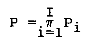
- a further reduction in effort results in the interpolation filter IPF being implemented by means of a cascade of sub-filters connected in series with I interpolation sub-factors P i , where and meaningfully P i (> 1) is an integer.
Landscapes
- Transmitters (AREA)
- Stabilization Of Oscillater, Synchronisation, Frequency Synthesizers (AREA)
- Digital Transmission Methods That Use Modulated Carrier Waves (AREA)
- Liquid Crystal Substances (AREA)
- Oscillators With Electromechanical Resonators (AREA)
- Optical Communication System (AREA)
- Analogue/Digital Conversion (AREA)
Description
Solche Verfahren sind bekannt, beispielsweise aus der Europäischen Offenlegungsschrift EP-A-508 661, die einen FM-Modulator beschreibt, der zur Erzeugung eines frequenzmodulierten Signales digitale Mittel in beschränkter Form benutzt, z.B. einen rückgekoppelten Phasenakkumulator zur Erzeugung eines digitalen frequenzmodulierten Signales und einen Trägeroszillator, welcher aus einer Tabelle Sinus- oder Cosinuswerte der Trägerschwingung ausliest. Dieser bekannte FM-Modulator gestattet zwar die beliebige Einstellung von Frequenzhub und Mittenfrequenz und zwar unabhängig voneinander, weist aber eine Reihe von Nachteilen auf wie z.B. Drift- und Alterungs- Probleme, nichtlineare Verzerrungen, das Erfordernis eines Abgleiches usw., welche alle daher rühren, daß der wesentliche Schaltungsaufwand dieses Modulators auf analoge Weise realisiert ist.

j =
Das FM-Signal g(k) ist idealerweise nicht bandbegrenzt, weshalb es durch ein Filter F mit komplexen Koeffizienten so bandzubegrenzen ist, daß die Systemanforderungen bezüglich Nachbarkanalstörungen eingehalten werden (bei UKW Bandbreite 300 kHz): Das Ergebnis am Filterausgang d(k).
Danach folgt ein Interpolations-Filter CIPF mit komplexen Koeffizienten, welches die Abtastfrequenz fA um den erforderlichen Faktor L erhöht, so daß am Filterausgang nur das gewünschte FM-Signal y(kT/L) um
Wird nun im System nur ein reelles FM-Signal benötigt, so wird lediglich der Realteil oder der Imaginärteil weiter verwendet. Gegebenenfalls kann eine Digital-Analog-Umsetzung erforderlich sein, der dann üblicherweise ein analoges Glättungs-Filter ABP (meistens Tiefpass, aber auch Bandpass) folgt.
Durch die Fouriertransformation sind Übertragungsfunktion und Impulsantwort bzw. Frequenz- und Zeitbereich miteinander verbunden:

Wird nur der Real- oder Imaginärteil weiter verwendet, so ergibt sich das Spektrum Y gemäß Figur 2d. Dieses Spektrum Y ist mit den gezeichneten Spektren symmetrisch sowohl bezüglich f = 0 als auch fA'/2 = 2fA, da es sich hier im Unterschied zur Figur 2a bis 2c um ein reelles Signal handelt. Dasselbe gilt auch für das analoge Signal y(t) beziehungsweise für sein Spektrum |Y| nach einer Digital-Analog-Umsetzung DAU mit nachfolgendem Glättungs-Filter ABP, siehe Figur 2e.
Daher kann das modulierende Digital-Signal v(kT) auch mit niedrigerer Abtastfrequenz fA/P angeliefert werden mit
In diesem Fall ist an beliebiger Stelle zwischen Quelle Q bzw. nach dem Analog-Digital-Umsetzer ADU und dem komplexen Oszillator COSZ die Abtastfrequenz mittels eines Interpolations-Filters oder durch eine Kaskade von mehreren um den Faktor P zu erhöhen.
Die Tabelle des komplexen Oszillators COSZ kann in folgenden Varianten aufgebaut sein:
Deutsches Patent 40 26 476.9.
Die komplexen Filter F und CIPF können zu einem einzigen komplexwertigen Filter zusammengefaßt werden, was ebenfalls eine Aufwandsverminderung sein kann.
Claims (13)
- Verfahren zur FM-Modulation eines digitalen Trägersignals (fc) mit einem digitalen NF-Signal v(kT) mittels eines rückgekoppelten Phasenakkumulators und eines Trägeroszillators, welcher numerisch gesteuert die Abtastwerte der modulierten FM-Schwingung bzw. des FM-Signals erzeugt, dadurch gekennzeichnet, daß das modulierende NF-Signal, mit der Abtastrate fA/P abgetastet wird mit P > 1,daß vor oder nach dem rückgekoppelten Phasenakkumulator mittels eines eingefügten Interpolationsfilters (IPF) die Abtastrate um den Faktor P interpoliert (erhöht) und das NF-Signal gefiltert wird,daß als Trägeroszillator ein komplexer Oszillator mit der Abtastrate fA arbeitet, ein komplexwertiges FM-Trägersignal (g(kT)) erzeugt, wobei die modulatorausgangsseitige Trägerfrequenz des nichtmodulierten Trägers fC = M · fA/P + f0 mit der ganzen Zahl M > 1 und f0 eine Hilfsfrequenz sind, unddaß anschließend mittels eines komplexwertigen Filters (F) eine Bandbegrenzung des komplexwertigen FM-Trägersignales (g(kT)) erfolgt (d(kT); y(kT)).
- Verfahren nach Anspruch 1, dadurch gekennzeichnet, daß diese Bandbegrenzung des FM-Signals auf die UKW-Bandbreite von 300 kHz erfolgt.
- Verfahren nach Anspruch 1 oder 2, dadurch gekennzeichnet, daß aus diesem bandbegrenzten FM-Signal (y) durch Berechnung des Real- oder Imaginärteils ein reellwertiges FM-Ausgangs-Signal (y(kT)) erzeugt wird.
- Verfahren nach Anspruch 3, dadurch gekennzeichnet, daß das reellwertige FM-Ausgangs-Signal digital- analog- umgesetzt wird.
- Verfahren nach Anspruch 4, dadurch gekennzeichnet, daß das analoge FM-Ausgangs-Signal mittels eines analogen Glättungsfilters (ABP, ATP) geglättet wird (y(t)).
- Verfahren nach einem der vorhergehenden Ansprüche, dadurch gekennzeichnet, daß an einer beliebigen Stelle vor dem komplexen Oszillator (COSZ) eine Multiplikation mit 2π erfolgt.
- Verfahren nach einem der vorhergehenden Ansprüche, dadurch gekennzeichnet, daß vor dem Phasenakkumulator eine Konstante fC/fA bzw. 2π fC/fA addiert wird zur Festlegung der ausgangsseitigen Mittenfrequenz fC des modulierten FM-Signals.
- Verfahren nach einem der vorhergehenden Ansprüche, dadurch gekennzeichnet, daß im komplexen Oszillator (COSZ) die Abtastwerte der modulierten FM-Schwingung aus einer Tabelle ausgelesen werden.
- Verfahren nach Anspruch 8, dadurch gekennzeichnet, daß die Tabelle des komplexen Oszillators (COSZ) zwei Teile mit gleichem Inhalt aber mit unterschiedlichen Adressen enthält, die zur Lieferung des Real- und Imaginärteils des komplexwertigen FM-Trägersignals gleichzeitig angesteuert und ausgelesen werden.
- Verfahren nach Anspruch 8, dadurch gekennzeichnet, daß die Tabelle des komplexen Oszillators (COSZ) aus einem Sinus- und einem Cosinusteil besteht, die unter der gleichen Adresse jeweils gleichzeitig angesteuert und ausgelesen werden.
- Verfahren nach Anspruch 8, dadurch gekennzeichnet, daß die Tabelle des komplexen Oszillators (COSZ) nur eine einzige Werttabelle für Real- und Imaginärteil umfaßt, die sequentiell angesteuert und ausgelesen werden.
- Verfahren nach einem der Ansprüche 1 bis 7, dadurch gekennzeichnet, daß die aktuellen Abtastwerte der komplexen FM-Schwingung jeweils mittels eines speziellen Rechenwerkes berechnet werden.
- Verfahren nach einem der vorhergehenden Ansprüche, dadurch gekennzeichnet, daß P eine ganze Zahl ist.
Applications Claiming Priority (2)
| Application Number | Priority Date | Filing Date | Title |
|---|---|---|---|
| DE4320999 | 1993-06-24 | ||
| DE19934320999 DE4320999C2 (de) | 1993-06-24 | 1993-06-24 | Verfahren zur Frequenzmodulation |
Publications (3)
| Publication Number | Publication Date |
|---|---|
| EP0631376A2 EP0631376A2 (de) | 1994-12-28 |
| EP0631376A3 EP0631376A3 (de) | 1995-11-08 |
| EP0631376B1 true EP0631376B1 (de) | 1998-12-16 |
Family
ID=6491121
Family Applications (1)
| Application Number | Title | Priority Date | Filing Date |
|---|---|---|---|
| EP94108901A Expired - Lifetime EP0631376B1 (de) | 1993-06-24 | 1994-06-10 | Verfahren zur Frequenzmodulation |
Country Status (4)
| Country | Link |
|---|---|
| EP (1) | EP0631376B1 (de) |
| AT (1) | ATE174733T1 (de) |
| DE (1) | DE59407477D1 (de) |
| ES (1) | ES2127849T3 (de) |
Families Citing this family (1)
| Publication number | Priority date | Publication date | Assignee | Title |
|---|---|---|---|---|
| FR2810814B1 (fr) | 2000-06-26 | 2002-09-20 | St Microelectronics Sa | Modulateur fm numerique a faible cout |
Family Cites Families (5)
| Publication number | Priority date | Publication date | Assignee | Title |
|---|---|---|---|---|
| JPH071850B2 (ja) * | 1985-09-12 | 1995-01-11 | 松下電器産業株式会社 | デイジタル処理fm変調装置 |
| KR940005374B1 (ko) * | 1989-04-07 | 1994-06-17 | 샤프 가부시끼가이샤 | Fm 변조기 |
| DE4026476C2 (de) * | 1990-08-22 | 1993-10-14 | Ant Nachrichtentech | Komplexes Polyphasennetzwerk |
| EP0508661A1 (de) * | 1991-04-11 | 1992-10-14 | Harris Corporation | FM-Modulatorschaltung mit getrennten Modulations- und Kanalsignalwegen |
| US5111163A (en) * | 1991-05-06 | 1992-05-05 | Hughes Aircraft Company | Digital FM modulator |
-
1994
- 1994-06-10 ES ES94108901T patent/ES2127849T3/es not_active Expired - Lifetime
- 1994-06-10 EP EP94108901A patent/EP0631376B1/de not_active Expired - Lifetime
- 1994-06-10 AT AT94108901T patent/ATE174733T1/de not_active IP Right Cessation
- 1994-06-10 DE DE59407477T patent/DE59407477D1/de not_active Expired - Fee Related
Also Published As
| Publication number | Publication date |
|---|---|
| EP0631376A2 (de) | 1994-12-28 |
| DE59407477D1 (de) | 1999-01-28 |
| EP0631376A3 (de) | 1995-11-08 |
| ES2127849T3 (es) | 1999-05-01 |
| ATE174733T1 (de) | 1999-01-15 |
Similar Documents
| Publication | Publication Date | Title |
|---|---|---|
| DE3784675T2 (de) | Schaltung zur rueckgewinnung von traegersignalen. | |
| DE2721850C2 (de) | Filter- und Demodulationsanordnung | |
| DE2003712C3 (de) | N-Pfad-Filter unter Verwendung eines Digitalfilters als zeitinvarianter Bestandteil | |
| EP0084876A2 (de) | Demodulatoranordnung zur Demodulation von in Frequenzmodulation auf einer Trägerfrequenzwelle enthaltener Signale | |
| DE2645950C2 (de) | Empfänger für ein frequenzmoduliertes HF-Eingangs-Signal | |
| EP0255553A1 (de) | Empfangsverfahren für frequenzmodulierte Stereo-Multiplex-Signale | |
| EP0308520B1 (de) | Digitaler Demodulator | |
| DE3784930T2 (de) | Empfaenger mit zwei zweigen. | |
| DE936097C (de) | Empfangsanordnung fuer eine Nachricht mehrdeutig darstellende elektrische Signale | |
| EP0261479B1 (de) | Optischer Überlagerungsempfänger | |
| DE2703566B2 (de) | Frequenzmodulationssystem | |
| DE69535211T2 (de) | Einrichtung zur kontinuierlichen phasenmodulation mit frequenzsynthetisierer mit phasenregelscheife | |
| DE2932961A1 (de) | Verfahren und schaltungsanordnung zur wiedergewinnung der traegerfrequenz aus einem modulierten elektrischen eingangssignal | |
| DE2933693C2 (de) | Bandpaßfilterschaltung | |
| EP0631377B1 (de) | Verfahren zur Frequenzmodulation | |
| EP0631378B1 (de) | Verfahren zur Frequenzmodulation | |
| DE2201391C3 (de) | Anordnung für Frequenzumsetzung von analogen Signalen | |
| EP0632576B1 (de) | Verfahren zur Frequenzmodulation | |
| EP0651526A2 (de) | Verfahren zur Aufbereitung eines digitalen Frequenzmultiplexsignals | |
| DE4320996C2 (de) | Verfahren zur Frequenzmodulation | |
| EP0631376A2 (de) | Verfahren zur Frequenzmodulation | |
| DE3208480A1 (de) | Traegerfrequenzrueckgewinnungseinrichtung fuer modulationssignale mit 2- oder -4-stufiger phasenverschiebung | |
| DE4320999A1 (de) | Verfahren zur Frequenzmodulation | |
| DE4321000C2 (de) | Verfahren zur Frequenzmodulation | |
| DE4320997C2 (de) | Verfahren zur Frequenzmodulation |
Legal Events
| Date | Code | Title | Description |
|---|---|---|---|
| PUAI | Public reference made under article 153(3) epc to a published international application that has entered the european phase |
Free format text: ORIGINAL CODE: 0009012 |
|
| AK | Designated contracting states |
Kind code of ref document: A2 Designated state(s): AT CH DE ES FR GB IT LI NL |
|
| PUAL | Search report despatched |
Free format text: ORIGINAL CODE: 0009013 |
|
| AK | Designated contracting states |
Kind code of ref document: A3 Designated state(s): AT CH DE ES FR GB IT LI NL |
|
| RAP1 | Party data changed (applicant data changed or rights of an application transferred) |
Owner name: ROBERT BOSCH GMBH |
|
| 17P | Request for examination filed |
Effective date: 19960508 |
|
| GRAG | Despatch of communication of intention to grant |
Free format text: ORIGINAL CODE: EPIDOS AGRA |
|
| 17Q | First examination report despatched |
Effective date: 19980225 |
|
| GRAG | Despatch of communication of intention to grant |
Free format text: ORIGINAL CODE: EPIDOS AGRA |
|
| GRAH | Despatch of communication of intention to grant a patent |
Free format text: ORIGINAL CODE: EPIDOS IGRA |
|
| GRAH | Despatch of communication of intention to grant a patent |
Free format text: ORIGINAL CODE: EPIDOS IGRA |
|
| GRAA | (expected) grant |
Free format text: ORIGINAL CODE: 0009210 |
|
| AK | Designated contracting states |
Kind code of ref document: B1 Designated state(s): AT CH DE ES FR GB IT LI NL |
|
| REF | Corresponds to: |
Ref document number: 174733 Country of ref document: AT Date of ref document: 19990115 Kind code of ref document: T |
|
| REG | Reference to a national code |
Ref country code: CH Ref legal event code: NV Representative=s name: SCINTILLA AG, DIREKTION Ref country code: CH Ref legal event code: EP |
|
| REF | Corresponds to: |
Ref document number: 59407477 Country of ref document: DE Date of ref document: 19990128 |
|
| ET | Fr: translation filed | ||
| ITF | It: translation for a ep patent filed | ||
| GBT | Gb: translation of ep patent filed (gb section 77(6)(a)/1977) |
Effective date: 19990223 |
|
| REG | Reference to a national code |
Ref country code: ES Ref legal event code: FG2A Ref document number: 2127849 Country of ref document: ES Kind code of ref document: T3 |
|
| PLBE | No opposition filed within time limit |
Free format text: ORIGINAL CODE: 0009261 |
|
| STAA | Information on the status of an ep patent application or granted ep patent |
Free format text: STATUS: NO OPPOSITION FILED WITHIN TIME LIMIT |
|
| 26N | No opposition filed | ||
| PGFP | Annual fee paid to national office [announced via postgrant information from national office to epo] |
Ref country code: GB Payment date: 20000719 Year of fee payment: 7 |
|
| PGFP | Annual fee paid to national office [announced via postgrant information from national office to epo] |
Ref country code: DE Payment date: 20010605 Year of fee payment: 8 |
|
| PG25 | Lapsed in a contracting state [announced via postgrant information from national office to epo] |
Ref country code: GB Free format text: LAPSE BECAUSE OF NON-PAYMENT OF DUE FEES Effective date: 20010610 |
|
| PGFP | Annual fee paid to national office [announced via postgrant information from national office to epo] |
Ref country code: FR Payment date: 20010622 Year of fee payment: 8 |
|
| PGFP | Annual fee paid to national office [announced via postgrant information from national office to epo] |
Ref country code: AT Payment date: 20010625 Year of fee payment: 8 |
|
| PGFP | Annual fee paid to national office [announced via postgrant information from national office to epo] |
Ref country code: NL Payment date: 20010626 Year of fee payment: 8 Ref country code: CH Payment date: 20010626 Year of fee payment: 8 |
|
| PGFP | Annual fee paid to national office [announced via postgrant information from national office to epo] |
Ref country code: ES Payment date: 20010629 Year of fee payment: 8 |
|
| GBPC | Gb: european patent ceased through non-payment of renewal fee |
Effective date: 20010610 |
|
| PG25 | Lapsed in a contracting state [announced via postgrant information from national office to epo] |
Ref country code: AT Free format text: LAPSE BECAUSE OF NON-PAYMENT OF DUE FEES Effective date: 20020610 |
|
| PG25 | Lapsed in a contracting state [announced via postgrant information from national office to epo] |
Ref country code: ES Free format text: LAPSE BECAUSE OF NON-PAYMENT OF DUE FEES Effective date: 20020611 |
|
| PG25 | Lapsed in a contracting state [announced via postgrant information from national office to epo] |
Ref country code: LI Free format text: LAPSE BECAUSE OF NON-PAYMENT OF DUE FEES Effective date: 20020630 Ref country code: CH Free format text: LAPSE BECAUSE OF NON-PAYMENT OF DUE FEES Effective date: 20020630 |
|
| PG25 | Lapsed in a contracting state [announced via postgrant information from national office to epo] |
Ref country code: NL Free format text: LAPSE BECAUSE OF NON-PAYMENT OF DUE FEES Effective date: 20030101 Ref country code: DE Free format text: LAPSE BECAUSE OF NON-PAYMENT OF DUE FEES Effective date: 20030101 |
|
| REG | Reference to a national code |
Ref country code: CH Ref legal event code: PL |
|
| PG25 | Lapsed in a contracting state [announced via postgrant information from national office to epo] |
Ref country code: FR Free format text: LAPSE BECAUSE OF NON-PAYMENT OF DUE FEES Effective date: 20030228 |
|
| NLV4 | Nl: lapsed or anulled due to non-payment of the annual fee |
Effective date: 20030101 |
|
| REG | Reference to a national code |
Ref country code: FR Ref legal event code: ST |
|
| REG | Reference to a national code |
Ref country code: ES Ref legal event code: FD2A Effective date: 20030711 |
|
| PG25 | Lapsed in a contracting state [announced via postgrant information from national office to epo] |
Ref country code: IT Free format text: LAPSE BECAUSE OF NON-PAYMENT OF DUE FEES;WARNING: LAPSES OF ITALIAN PATENTS WITH EFFECTIVE DATE BEFORE 2007 MAY HAVE OCCURRED AT ANY TIME BEFORE 2007. THE CORRECT EFFECTIVE DATE MAY BE DIFFERENT FROM THE ONE RECORDED. Effective date: 20050610 |