EP0613116A2 - Verfahren zum Steuern eines Flüssigkristallanzeigegeräts - Google Patents
Verfahren zum Steuern eines Flüssigkristallanzeigegeräts Download PDFInfo
- Publication number
- EP0613116A2 EP0613116A2 EP94102831A EP94102831A EP0613116A2 EP 0613116 A2 EP0613116 A2 EP 0613116A2 EP 94102831 A EP94102831 A EP 94102831A EP 94102831 A EP94102831 A EP 94102831A EP 0613116 A2 EP0613116 A2 EP 0613116A2
- Authority
- EP
- European Patent Office
- Prior art keywords
- selection
- potential
- period
- liquid crystal
- voltage
- Prior art date
- Legal status (The legal status is an assumption and is not a legal conclusion. Google has not performed a legal analysis and makes no representation as to the accuracy of the status listed.)
- Granted
Links
Images


Classifications
-
- G—PHYSICS
- G09—EDUCATION; CRYPTOGRAPHY; DISPLAY; ADVERTISING; SEALS
- G09G—ARRANGEMENTS OR CIRCUITS FOR CONTROL OF INDICATING DEVICES USING STATIC MEANS TO PRESENT VARIABLE INFORMATION
- G09G3/00—Control arrangements or circuits, of interest only in connection with visual indicators other than cathode-ray tubes
- G09G3/20—Control arrangements or circuits, of interest only in connection with visual indicators other than cathode-ray tubes for presentation of an assembly of a number of characters, e.g. a page, by composing the assembly by combination of individual elements arranged in a matrix no fixed position being assigned to or needed to be assigned to the individual characters or partial characters
- G09G3/34—Control arrangements or circuits, of interest only in connection with visual indicators other than cathode-ray tubes for presentation of an assembly of a number of characters, e.g. a page, by composing the assembly by combination of individual elements arranged in a matrix no fixed position being assigned to or needed to be assigned to the individual characters or partial characters by control of light from an independent source
- G09G3/36—Control arrangements or circuits, of interest only in connection with visual indicators other than cathode-ray tubes for presentation of an assembly of a number of characters, e.g. a page, by composing the assembly by combination of individual elements arranged in a matrix no fixed position being assigned to or needed to be assigned to the individual characters or partial characters by control of light from an independent source using liquid crystals
- G09G3/3611—Control of matrices with row and column drivers
- G09G3/3622—Control of matrices with row and column drivers using a passive matrix
- G09G3/3629—Control of matrices with row and column drivers using a passive matrix using liquid crystals having memory effects, e.g. ferroelectric liquid crystals
-
- G—PHYSICS
- G02—OPTICS
- G02F—OPTICAL DEVICES OR ARRANGEMENTS FOR THE CONTROL OF LIGHT BY MODIFICATION OF THE OPTICAL PROPERTIES OF THE MEDIA OF THE ELEMENTS INVOLVED THEREIN; NON-LINEAR OPTICS; FREQUENCY-CHANGING OF LIGHT; OPTICAL LOGIC ELEMENTS; OPTICAL ANALOGUE/DIGITAL CONVERTERS
- G02F1/00—Devices or arrangements for the control of the intensity, colour, phase, polarisation or direction of light arriving from an independent light source, e.g. switching, gating or modulating; Non-linear optics
- G02F1/01—Devices or arrangements for the control of the intensity, colour, phase, polarisation or direction of light arriving from an independent light source, e.g. switching, gating or modulating; Non-linear optics for the control of the intensity, phase, polarisation or colour
- G02F1/13—Devices or arrangements for the control of the intensity, colour, phase, polarisation or direction of light arriving from an independent light source, e.g. switching, gating or modulating; Non-linear optics for the control of the intensity, phase, polarisation or colour based on liquid crystals, e.g. single liquid crystal display cells
- G02F1/133—Constructional arrangements; Operation of liquid crystal cells; Circuit arrangements
-
- G—PHYSICS
- G09—EDUCATION; CRYPTOGRAPHY; DISPLAY; ADVERTISING; SEALS
- G09G—ARRANGEMENTS OR CIRCUITS FOR CONTROL OF INDICATING DEVICES USING STATIC MEANS TO PRESENT VARIABLE INFORMATION
- G09G3/00—Control arrangements or circuits, of interest only in connection with visual indicators other than cathode-ray tubes
- G09G3/20—Control arrangements or circuits, of interest only in connection with visual indicators other than cathode-ray tubes for presentation of an assembly of a number of characters, e.g. a page, by composing the assembly by combination of individual elements arranged in a matrix no fixed position being assigned to or needed to be assigned to the individual characters or partial characters
- G09G3/34—Control arrangements or circuits, of interest only in connection with visual indicators other than cathode-ray tubes for presentation of an assembly of a number of characters, e.g. a page, by composing the assembly by combination of individual elements arranged in a matrix no fixed position being assigned to or needed to be assigned to the individual characters or partial characters by control of light from an independent source
- G09G3/36—Control arrangements or circuits, of interest only in connection with visual indicators other than cathode-ray tubes for presentation of an assembly of a number of characters, e.g. a page, by composing the assembly by combination of individual elements arranged in a matrix no fixed position being assigned to or needed to be assigned to the individual characters or partial characters by control of light from an independent source using liquid crystals
- G09G3/3611—Control of matrices with row and column drivers
- G09G3/3674—Details of drivers for scan electrodes
- G09G3/3681—Details of drivers for scan electrodes suitable for passive matrices only
-
- G—PHYSICS
- G09—EDUCATION; CRYPTOGRAPHY; DISPLAY; ADVERTISING; SEALS
- G09G—ARRANGEMENTS OR CIRCUITS FOR CONTROL OF INDICATING DEVICES USING STATIC MEANS TO PRESENT VARIABLE INFORMATION
- G09G3/00—Control arrangements or circuits, of interest only in connection with visual indicators other than cathode-ray tubes
- G09G3/20—Control arrangements or circuits, of interest only in connection with visual indicators other than cathode-ray tubes for presentation of an assembly of a number of characters, e.g. a page, by composing the assembly by combination of individual elements arranged in a matrix no fixed position being assigned to or needed to be assigned to the individual characters or partial characters
- G09G3/34—Control arrangements or circuits, of interest only in connection with visual indicators other than cathode-ray tubes for presentation of an assembly of a number of characters, e.g. a page, by composing the assembly by combination of individual elements arranged in a matrix no fixed position being assigned to or needed to be assigned to the individual characters or partial characters by control of light from an independent source
- G09G3/36—Control arrangements or circuits, of interest only in connection with visual indicators other than cathode-ray tubes for presentation of an assembly of a number of characters, e.g. a page, by composing the assembly by combination of individual elements arranged in a matrix no fixed position being assigned to or needed to be assigned to the individual characters or partial characters by control of light from an independent source using liquid crystals
- G09G3/3611—Control of matrices with row and column drivers
- G09G3/3685—Details of drivers for data electrodes
- G09G3/3692—Details of drivers for data electrodes suitable for passive matrices only
-
- G—PHYSICS
- G09—EDUCATION; CRYPTOGRAPHY; DISPLAY; ADVERTISING; SEALS
- G09G—ARRANGEMENTS OR CIRCUITS FOR CONTROL OF INDICATING DEVICES USING STATIC MEANS TO PRESENT VARIABLE INFORMATION
- G09G2300/00—Aspects of the constitution of display devices
- G09G2300/04—Structural and physical details of display devices
- G09G2300/0469—Details of the physics of pixel operation
- G09G2300/0478—Details of the physics of pixel operation related to liquid crystal pixels
- G09G2300/0482—Use of memory effects in nematic liquid crystals
- G09G2300/0486—Cholesteric liquid crystals, including chiral-nematic liquid crystals, with transitions between focal conic, planar, and homeotropic states
-
- G—PHYSICS
- G09—EDUCATION; CRYPTOGRAPHY; DISPLAY; ADVERTISING; SEALS
- G09G—ARRANGEMENTS OR CIRCUITS FOR CONTROL OF INDICATING DEVICES USING STATIC MEANS TO PRESENT VARIABLE INFORMATION
- G09G2310/00—Command of the display device
- G09G2310/06—Details of flat display driving waveforms
-
- G—PHYSICS
- G09—EDUCATION; CRYPTOGRAPHY; DISPLAY; ADVERTISING; SEALS
- G09G—ARRANGEMENTS OR CIRCUITS FOR CONTROL OF INDICATING DEVICES USING STATIC MEANS TO PRESENT VARIABLE INFORMATION
- G09G2310/00—Command of the display device
- G09G2310/06—Details of flat display driving waveforms
- G09G2310/061—Details of flat display driving waveforms for resetting or blanking
-
- G—PHYSICS
- G09—EDUCATION; CRYPTOGRAPHY; DISPLAY; ADVERTISING; SEALS
- G09G—ARRANGEMENTS OR CIRCUITS FOR CONTROL OF INDICATING DEVICES USING STATIC MEANS TO PRESENT VARIABLE INFORMATION
- G09G2310/00—Command of the display device
- G09G2310/06—Details of flat display driving waveforms
- G09G2310/065—Waveforms comprising zero voltage phase or pause
-
- G—PHYSICS
- G09—EDUCATION; CRYPTOGRAPHY; DISPLAY; ADVERTISING; SEALS
- G09G—ARRANGEMENTS OR CIRCUITS FOR CONTROL OF INDICATING DEVICES USING STATIC MEANS TO PRESENT VARIABLE INFORMATION
- G09G2320/00—Control of display operating conditions
- G09G2320/02—Improving the quality of display appearance
- G09G2320/0247—Flicker reduction other than flicker reduction circuits used for single beam cathode-ray tubes
-
- G—PHYSICS
- G09—EDUCATION; CRYPTOGRAPHY; DISPLAY; ADVERTISING; SEALS
- G09G—ARRANGEMENTS OR CIRCUITS FOR CONTROL OF INDICATING DEVICES USING STATIC MEANS TO PRESENT VARIABLE INFORMATION
- G09G2320/00—Control of display operating conditions
- G09G2320/04—Maintaining the quality of display appearance
- G09G2320/041—Temperature compensation
-
- G—PHYSICS
- G09—EDUCATION; CRYPTOGRAPHY; DISPLAY; ADVERTISING; SEALS
- G09G—ARRANGEMENTS OR CIRCUITS FOR CONTROL OF INDICATING DEVICES USING STATIC MEANS TO PRESENT VARIABLE INFORMATION
- G09G2320/00—Control of display operating conditions
- G09G2320/10—Special adaptations of display systems for operation with variable images
Definitions
- the present invention relates to a method of driving a liquid crystal display device that uses a chiral nematic liquid crystal having two metastable states. More specifically, it relates to a drive method that improves the speed of writing. The present invention also relates to a drive method that can compensate the drive voltage to cope with irregularities in the threshold value of the liquid crystal that are specific to each liquid crystal panel, and provide temperature compensation of the drive voltage. The present invention further relates to a drive method that ameliorates the imbalance between the voltages of two different drive waveforms and makes it possible to turn the drive circuitry into an Integrated Circuit chip (IC).
- IC Integrated Circuit chip
- the first method obtains the two metastable states as follows: a 360 ° twist orientation state is obtained by using a toggle switch to suddenly turn off the voltage (60 Hz, 15 V peak-to-peak) applied to the liquid crystal; and a 0 uniform orientation state is obtained by using a variable-voltage device to allow the voltage applied to the liquid crystal to slowly fall over approximately 1 second.
- the second method is as follows: if a high frequency of 1500 kHz is applied directly to the liquid crystal after a low-frequency field is turned off, a 360 twist orientation state is enabled. If the 1500-kHz high-frequency field is applied after a delay of approximately 1/4 second after the same low-frequency field has been turned off, a 0 uniform orientation state is achieved.
- the first method is completely impracticable; it can never progress beyond simple verification in the laboratory.
- the present inventors came to experiment with the latter method, they discovered that, if a high-frequency field is applied after a delay of approximately 1/4 second after the low-frequency field has been turned off, the same 360 twist orientation state is achieved, and it was thus impossible to switch between the two metastable states.
- Japanese Laid-Open Publication 1-51818 states nothing about a matrix display which is currently most appropriate for practical use and has high quality as a display device, and disclosed nothing about a drive method for such a device.
- irregularities in the drive characteristics that are induced during the process of fabricating a liquid crystal display panel include differences in drive characteristics that depend on position within any one display panel and differences in drive characteristics between different display panels caused by differences between manufacturing lots. Therefore, to ensure that a whole liquid crystal display screen can be used with its display quality always optimized, it is necessary to provide subtle control of the drive voltage to match each panel. In addition, even if the optimal adjustment has been achieved by some method, new changes in the drive conditions are likely to be caused by variations in the surrounding temperature, so it is essential to provide further adjustment to match temperature variations.
- Fig. 49 Differences in the threshold value of the drive voltage within a single panel are shown in Fig. 49. Since the drive voltage varies in this manner in response to small differences in orientation state or variations in cell gap, an optimal adjustment of the drive voltage must be done for each panel to accommodate its worst area. Variations in drive voltage with respect to temperature variations that are assumed likely to occur for a matrix drive are shown in Fig. 18. The gradient of the curve with respect to temperature is low at 0.02 V/ ° C, but, if a voltage change ratio of 0.56%/ ° C is considered based on a drive voltage of 25 ° C, this becomes fairly large at 19.6% over an actual temperature range of 5 to 40 ° C. This looks promising for compensation to the optimal display in practical use.
- It is an object of the present invention is to provide a highly practicable method of driving a liquid crystal that shortens the write time and prevents flickering of the display when it is used to drive a chiral nematic liquid crystal having a memory capability.
- Another object of the present invention is to shorten the time required to write one line of data and thus provide a method of driving a liquid crystal with a high duty ratio such that it can be applied to a large- screen liquid crystal panel.
- a further object of the present invention is to provide a method of driving a liquid crystal that can compensate for fabrication-induced irregularities in the threshold value of the liquid crystal within the liquid crystal panel, or for variations in drive voltage caused by ambient temperature.
- a still further object of the present invention is to provide a method of driving a liquid crystal that can reduce the imbalance between the voltages of the scan and data signals, simplify the configuration of the drive circuitry, and make the drive circuitry suitable for incorporation in ICs, even when a reset voltage of a comparatively large absolute value is applied to the liquid crystal.
- the method of the present invention relates to a method of driving a liquid crystal display device that uses a chiral nematic liquid crystal medium wherein liquid crystal molecules interposed between substrates have a predetermined angle of twist in an initial state, and wherein the chiral nematic liquid crystal medium has two metastable states that differ from the initial state as relaxation states after a voltage that brings about a Frederick's transition is applied to the liquid crystal while it is in the initial state.
- This method is characterized in comprising the following four steps (a-d), which are to be read with Figs. 2A-2B:
- the length of selection period T3 is shortened by the addition of delay period T2; in other words, it can shorten the write time.
- the length of the delay period may be set such that the selection voltage is applied to the liquid crystal at a time in the vicinity of a transition point to the two metastable states, after backflow has occurred and the liquid crystal molecules at the approximate center between the substrates have relaxed into one of the metastable states from a homeotropic orientation state, directly after the application of the reset voltage has ended.
- the orientation state of the liquid crystal is determined to be either of two metastable states by the appropriate application of a trigger after backflow has occurred in the liquid crystal.
- a difference signal Yn-Xm (which expresses the difference between a row electrode signal Yn and a column electrode signal Xm) is made to include, within one frame period, a selection period T3 that sets each row electrode in sequence, a subsequent nonselection period T4, a reset period T1 that is set before selection period T3, and a delay period T2 that is set between reset period T1 and selection period T3, as shown in Figs. 8A-8D.
- row electrode signal Yn is at a reset potential Vr during reset period T1, at a selection potential (e.g., ⁇ 2Vb) during selection period T3, and at a nonselection potential (e.g., 0 V) during nonselection period T4.
- Column electrode signal Xm is set to the data potential of either an ON selection potential or an OFF selection potential (e.g., ⁇ Vb) in synchronization with selection period T3.
- the present invention can also be applied to a method in which selection period T3 after delay period T2 is handled as a first selection period, and a pair of periods comprising an interval period T5 when a nonselection voltage 34 is applied to the liquid crystal and a second selection period T6 when selection voltage 32 is applied to the liquid crystal, is provided either once or a plurality of times between this first selection period T3 and nonselection period T4, as shown in Fig. 9A or Fig. 9B.
- the liquid crystal having a memory capability that is the target of the present invention utilizes a cumulative pulse response effect within an extremely short period, such as 1 to 2 ms after the reset voltage has been turned off. Therefore, even if the selection pulse is divided into a plurality of pulses, display is enabled in the same manner as if there were only one pulse. It should be noted that this divided selection pulse drive can also be applied to a drive method in which no delay period T2 is set within the period T of one frame, as shown in Fig. 13.
- the delay period may be set to (1 H/2) x n (where n is an integer) for an alternating drive wherein the polarity of the voltage applied to the liquid crystal is inverted at each pulse, from consideration of the fact that the pulse width is 1 H/2.
- the duty ratio of a period of the selection potential with respect to selection period T3 of row electrode signal Yn and/or the duty ratio of a period t_ of the data potential with respect to selection period T3 of column electrode signal Xm can be set to less than 100%, as shown in Figs. 14, 16, 17, and 19.
- Changing the duty ratio of the total pulse width t of the selection pulse(s) with respect to selection period T3 can provide the same effect, so long as the RMS voltage does not change within selection period T3. If the peak voltage value of the selection pulse is increased by reducing the duty ratio, drive voltage accuracy of the circuitry can be made easier to achieve. Similarly, if the duty ratio of the pulse is varied with the drive voltage kept constant, it is clear that the display effect can be varied by causing variations in the RMS value. In other words, by changing the duty ratio, the method of the present invention can compensate for subtle differences in drive voltage attributed to irregularities in the threshold value of the liquid crystal within the display panel, such as those shown in Fig. 49. The threshold value of the liquid crystal is also affected by temperature, so that varying the duty ratio can also enable temperature compensation.
- At least one of the row electrode signals supplied to a plurality of the row electrodes respectively can be set such that the duty ratio of the period of the selection potential with respect to the selection period has a different value from that of the other row electrode signals. This can compensate for differences in drive voltage attributed to irregularities in the threshold value of the liquid crystal at the top and bottom of the liquid crystal panel.
- At least one of the column electrode signals supplied to a plurality of the column electrodes could be set such that the duty ratio of the data potential period with respect to the selection period has a different value from that of the other column electrode signals. This can compensate for differences in drive voltage attributed to irregularities in the threshold value of the liquid crystal at the left and right sides of the liquid crystal panel.
- a column electrode signal could be adjusted such that the duty ratio of the period of the data potential with respect to the selection period corresponding to one pixel on one of the column electrodes that is supplied with one of the column electrode signals is set to be different from that of the selection periods corresponding to the other pixels on the one column electrode. This can compensate for differences in drive voltage attributed to irregularities in the threshold value of the liquid crystal at the top and bottom of each column of the liquid crystal panel.
- the above described changing of the duty ratio of the selection pulse width with respect to the selection period is not necessarily limited to application to a drive waveform that specifies delay period T2 within a frame period.
- it is also effective for changing the duty ratio of the above described drive waveform shown in Fig. 3 that does not specify delay period T2.
- the present invention can also compensate for irregularities in the threshold value of the liquid crystal or changes in the threshold value of the liquid crystal dependent on ambient temperature, by changing a parameter relating to a state in which the selection voltage is imposed that can change the threshold value of the liquid crystal.
- the delay period can be varied either manually or automatically as this parameter.
- the delay time could be set to be long when the threshold value of the liquid crystal is high, but short when the threshold value of the liquid crystal is low.
- the delay time could be set to be short when the detected ambient temperature is high, but long when the ambient temperature is low, so that the threshold value of the liquid crystal can be maintained within a constant range, regardless of the ambient temperature.
- the selection voltage can be varied either manually or automatically as this parameter.
- the absolute value of the selection voltage could be set to be large when the threshold value of the liquid crystal is high, but small when the threshold value of the liquid crystal is low.
- the absolute value of the selection voltage could be set to be small when the detected ambient temperature is high, but large when the ambient temperature is low, so that the threshold value of the liquid crystal can be maintained within a constant range, regardless of the ambient temperature.
- the length of selection period dependent on the drive frequency can be varied either manually or automatically as this parameter.
- the drive frequency can be set to be low and thus the selection period long when the threshold value of the liquid crystal is high, and the drive frequency can be set to be high and thus the selection period short when the threshold value of the liquid crystal is low.
- the drive frequency can be set to be high when the detected ambient temperature is high, but low when the ambient temperature is low, so that the threshold value of the liquid crystal can be maintained within a constant range, regardless of the ambient temperature.
- the duty ratio with respect to the selection period of the period during which the selection voltage is applied to the liquid crystal can be varied either manually or automatically as this parameter.
- the duty ratio could be set to be high when the threshold value of the liquid crystal is high, but low when the threshold value of the liquid crystal is low.
- the duty ratio could be set to be low when the detected ambient temperature is high, but high when the ambient temperature is low, so that the threshold value of the liquid crystal can be maintained within a constant range, regardless of the ambient temperature.
- a working temperature region could be divided into a plurality of temperature ranges, a parameter could be preset to have a different value within each of these temperature ranges, and temperature compensation could be provided by selecting a setting for the predetermined parameter in the temperature range that the ambient temperature belongs to.
- the present invention can also provide a seven-level drive method.
- This seven-level drive method enables the drive of a liquid crystal using seven levels of potential: two types of potential (e.g., ⁇ Vb) are set as data potentials of column electrode signal Xm (as shown in Figs. 8A-8D) for applying an ON or OFF selection voltage to the liquid crystal, two types of potential (e.g., ⁇ Vr) are set as data potentials for row electrode signal Yn for applying either a positive or negative reset voltage to the liquid crystal during reset period T1, two types of potential (e.g., ⁇ 2Vb) are set as selection potentials for applying either a positive or negative selection voltage to the liquid crystal during selection period T3, and a potential intermediate between the two types of selection potential (e.g., 0 V) is set as a nonselection potential during the delay period and the nonselection period.
- two types of potential e.g., ⁇ Vb
- Xm as shown in Figs. 8A-8D
- ⁇ Vr data potentials for row electrode signal
- the present invention can be applied to a drive method that comprises at least eight levels.
- An eight-level drive method enables the drive of a liquid crystal using at least eight levels of potential: four types of potential are set as data potentials of the column electrode signal for applying positive or negative ON selection voltages and positive and negative OFF selection voltages to the liquid crystal, two types of potential are set as reset potentials of the row electrode signal for applying positive and negative reset voltages to the liquid crystal during the reset period, two types of potential are set as selection potentials for applying positive and negative selection voltages to the liquid crystal during the selection period, two types of data potential are set as nonselection potentials for imparting bias potentials to the above four types of the data potential during the delay period and the nonselection period, and either two types of the selection potential or two potentials among four types of data potential set to be the same as two types of the reset potential.
- V1, V2, V3, and V4 These eight levels of potential are divided into four levels in a first, low-voltage group (V1, V2, V3, and V4, where V1 ⁇ V2 ⁇ V3 ⁇ V4) and four levels in a second, high-voltage group (V5, V6, V7, and V8, where V4 ⁇ V5 ⁇ V6 ⁇ V7 ⁇ V8).
- the reset potential is selected from amongst the second group; when the data potential of the column electrode signal is in the second group, the reset potential is selected from amongst the first group.
- the absolute value of the reset voltage applied to the liquid crystal during the reset period can also be set to be large.
- the ON selection potential of column electrode signal Xm is set to V5 of the second group and the OFF selection potential is set to V7, as shown in Fig. 32.
- the reset potential of row electrode signal Yn is set to V1, the selection potential to V8, and the nonselection potential to V6.
- the ON selection potential of column electrode signal Xm is set to V4 of the first group and the OFF selection potential to V2.
- the reset potential of row electrode signal Yn is set to V8, the selection potential to V1, and the nonselection potential to V3, thus enabling an alternating drive for the liquid crystal in which the polarity is inverted every frame.
- the ON selection potential of column electrode signal Xm is set to V8 of the second group and the OFF selection potential to V6, as shown in Fig. 33.
- the reset potential of row electrode signal Yn is set to V1, the selection potential to V5, and the nonselection potential to V7.
- the ON selection potential of column electrode signal Xm is set to V1 of the first group and the OFF selection potential to V3.
- the reset potential of row electrode signal Yn is set to V8, the selection potential to V4, and the nonselection potential to V2, thus enabling an alternating drive for the liquid crystal in which the polarity is inverted every frame.
- the ON selection potential of column electrode signal Xm within one frame period T is set by alternating pulses between V4 and V5
- the OFF selection potential of column electrode signal Xm is set by alternating pulses between V2 and V7, as shown in Fig. 34.
- the reset potential of row electrode signal Yn is set by alternating pulses between V8 and V1
- the selection potential by alternating pulses between V1 and V8 and the nonselection potential by alternating pulses between V3 and V6.
- the ON selection potential of column electrode signal Xm within one frame period T is set by alternating pulses between V1 and V8, and the OFF selection potential of column electrode signal Xm is set by alternating pulses between V3 and V6, as shown in Fig. 35.
- the reset potential of row electrode signal Yn is set by alternating pulses between V8 and V1, the selection potential by alternating pulses between V4 and V5, and the nonselection potential by alternating pulses between V2 and V7. This enables an alternating drive for the liquid crystal in which the polarity of the voltage applied to the liquid crystal is inverted at each pulse.
- a unit time equivalent to selection period T3 is termed 1 H
- the pulse width of a signal FR that causes the row and column electrode signals to alternate is also 1 H
- the phase of signal FR can be set to be offset by (1 H/2) with respect with the selection period of row electrode signal Yn.
- a drive method where this is applied to the drive method of Fig. 34 is shown in Fig. 36.
- the numbers of inversions of the drive potentials of the row and column electrode signals are half those of Fig. 34, but the number of inversions of the voltage applied to the liquid crystal can be guaranteed to be more.
- the polarity of the voltage applied to the liquid crystal is inverted at each unit time equivalent to selection period T3 (1 H) so that, if the polarity at the beginning of the kth frame (where k is an integer) is positive, the polarity at the beginning of the (k + 1 )th frame is made negative; if the polarity at the beginning of the kth frame is negative, the polarity at the beginning of the (k + 1)th frame is made positive.
- This enables an alternating drive for the liquid crystal in which polarity inversions every 1 H and every frame are combined.
- a drive method where this is applied to the drive method of Fig. 34 is shown in Fig. 37.
- the above described seven-level and eight-level drive methods are not necessarily limited to application to a drive waveform that specifies delay period T2 within one frame period T; they are also effective for the drive waveform shown in Fig. 3, which does not specify delay period T2.
- the liquid crystal medium used in each of the embodiments described below is formed by adding a chiral dopant (e.g., such as that available from E. Merck Corp. as product No. S811) to a nematic liquid crystal (e.g., such as that available from E. Merck Corp. as product No. ZLl3329), with the helical pitch of the liquid crystal being adjusted to 3 to 4 ⁇ m.
- a pattern of transparent electrodes 4 is formed of indium tin oxide (ITO) on upper and lower glass substrates 5, and a polyimide orientation film 2 (of, e.g., product SP-740 from Toray Corp.) is painted over each pattern.
- Spacers are inserted between upper and lower glass substrates 5 to ensure that the substrate gap is kept uniform at, e.g., a substrate gap (cell gap) of 2 ⁇ m or less.
- the ratio of the thickness of the liquid crystal layer to the twist pitch is 0.5 ⁇ 0.2.
- FIG. 2A shows an alternating drive waveform in which the polarity of the voltage that causes the liquid crystal cell to be charged is inverted once every frame period T.
- Fig. 2B shows an alternating drive waveform in which the polarity of the voltage that causes the liquid crystal cell to be charged is inverted once every pulse of pulse width (T3)/2.
- a reset voltage (reset pulse) 30 that is greater than or equal to the threshold value that brings about a Frederick's transition in nematic liquid crystal is applied during reset period T1.
- the peak value of reset voltage 30 is set to ⁇ 30 V.
- the reset period T2 is provided to delay the timing at which a selection voltage (selection pulse) 32 is applied to the liquid crystal cell during selection period T3, after reset voltage 30 has been applied to the liquid crystal cell.
- a voltage which is the same as nonselection voltage 33 e.g., is applied to the liquid crystal cell during delay period T2 as a delay voltage 31.
- Selection voltage 32 applied to the liquid crystal cell in selection period T3 is selected with reference to a critical value that causes either of two metastable states in the nematic liquid crystal, such as a 360 twist orientation state and a 0 uniform orientation state.
- a critical value that causes either of two metastable states in the nematic liquid crystal, such as a 360 twist orientation state and a 0 uniform orientation state.
- a drive waveform is shown in Fig. 3 as a comparative example.
- the drive waveform shown in Fig. 3 is that disclosed previously by the applicants of the present invention in US Patent Application Serial Nos. 08/059,226 and 08/093,290.
- the drive method of Fig. 3 is similar to those of Figs. 2A and 2B in that a reset period T1, a selection period T3, and a nonselection period T4 are provided within one frame period, but differs therefrom in that delay period T2 is not provided.
- the drive method of the first embodiment shown in Figs. 2A and 2B differs greatly from the drive method of Fig. 3 in that selection voltage 32 is applied to the liquid crystal cell after delay period T2 has elapsed after the application of reset voltage 30.
- the duty ratio is the ratio of (selection period T3)/(frame period T)
- the pulse width is that of the selection pulse
- the delay time is the length of delay period T2.
- the pulse width is equal to T3
- the pulse width is equal to (T3)/2.
- the write time for one line matches selection period T3.
- the ON voltage is the value of selection voltage 32 applied to the liquid crystal cell that causes the 0 uniform orientation state in the liquid crystal cell.
- the OFF voltage is the value of selection voltage 32 applied to the liquid crystal cell that causes the 360 ° twist orientation state.
- Fig. 4 The results of dynamic simulation of the behavior of a bistable liquid crystal used with the present invention, and the relationship between delay period T2 and selection period T3 are shown in Fig. 4.
- time is plotted along the X-axis
- the tilt of molecules at the center of the liquid crystal cell is plotted along the Y-axis, with a start point being the time at which the reset pulse is cut.
- backflow backward
- the former is a transition to a 0 uniform orientation state and the latter corresponds to a transition to a 360 ° twist orientation state where a twist is added to the change in tilt.
- selection period T3 is set immediately after reset period T1 has expired, as shown in Fig. 4.
- the liquid crystal can be turned on and off so long as this selection period T3 is extended as far as the timing at which this trigger ought to be imposed, after backflow has occurred in the liquid crystal.
- Table 1 shows that if the length of selection period T3 is set to either 400 us or 200 us, it is possible to switch the liquid crystal on and off, but if the length of selection period T3 is set to 100 us, it is no longer possible to switch the liquid crystal on and off.
- the drive method of Figs. 2A and 2B which concerns the drive method of the first embodiment makes it possible to apply selection voltage 32 to the liquid crystal at the timing at which this trigger ought to be imposed after backflow has ended, without having to adjust the length of selection period T3. That is why it becomes possible to switch the liquid crystal on and off with this embodiment, even when the length of selection period T3 is greatly reduced to 50 us, as shown in Table 2.
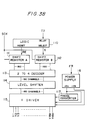
- a simple matrix type of liquid crystal display panel shown in Fig. 5 was fabricated using the liquid crystal cell shown in Fig. 1.
- This liquid crystal display panel is of a transparent type with a backlight 12 positioned at a back surface of a liquid crystal cell 11.
- a scan drive circuit 13 is connected to scan electrodes (row electrodes) of the liquid crystal cell 11, and this scan drive circuit 13 is controlled by a scan control circuit 15.
- signal electrodes (column electrodes) are connected to a signal drive circuit 14 of liquid crystal cell 11, and signal drive circuit 14 is controlled by a signal control circuit 16.
- a predetermined applied voltage from a potential setting circuit 17 is supplied to scan drive circuit 13 and signal drive circuit 14.
- a reference clock signal and a predetermined timing signal are supplied to scan control circuit 15 and signal control circuit 16 from a line sequential scan circuit 18.
- the drive waveform used to drive the simple matrix type of liquid crystal display panel of Fig. 5 is shown in Fig. 6.
- a bias voltage 34 is the same as nonselection voltage 33 during delay period T2 after reset voltage 30, and is inevitably applied when the pixels of other rows are selected.
- the length of selection period T3 matches one horizontal scanning period (1 H).
- the length of delay period T2 is set to be (1 H/2) x n (where n is an integer), from consideration of the fact that the drive alternates once every pulse of pulse width 1 H/2.
- FIG. 7 A graph used to obtain the selection voltage range that enables a 0 uniform orientation state and a 360 twist orientation state, using the drive waveform of Fig. 6, is shown in Fig. 7.
- Delay time is plotted along the X-axis and the voltage of pulses applied to the liquid crystal is plotted along the Y-axis.
- a liquid crystal cell of the same construction as that of the first embodiment was used, with the ratio of cell gap d to pitch p being 0.6.
- the delay time can be chosen to be where the ON voltage shown by the solid line in Fig. 7 lies below the ON selection voltage 3Vb shown by a broken line in Fig. 7 (hatched area in Fig. 7).
- Yn and Yn + 1 indicate scan signals (row electrode signals) for driving the nth and (n + 1)th row electrodes. These scan signals Yn and Yn + 1 are set to the reset potential at the peak value ⁇ Vr during reset period T1, to 0 V during delay period T2, to the selection potential at the peak value ⁇ 2Vb during selection period T3, and to the nonselection potential of 0 V during nonselection period T4.
- Xm indicates the waveform of the data signal supplied to the column electrode of the mth column. The peak value of this data signal is ⁇ Vb.
- the difference signal Yn-Xm indicates the drive waveform applied to the liquid crystal of the pixel at the intersection between the nth row electrode and the mth column electrode.
- This difference signal Yn-Xm is at reset voltage 30, which has a maximum peak value of ⁇ (Vr + Vb), during reset period T1, and at bias voltage 34, which has a maximum peak value of ⁇ Vb, during delay period T2.
- this signal is set to a selection voltage 32 for driving the liquid crystal at a peak value of ⁇ 3Vb during selection period T3, then to nonselection voltage 33 at a peak value of ⁇ Vb during nonselection period T4.
- the first and second embodiments have made it possible to achieve a faster write of 50 ⁇ s/line, which is of several times the prior art speed.
- the basic characteristics of the liquid crystal display device to which the present invention is directed must exceed those of supertwisted nematic (STN): such as a memory capability of several seconds; a contrast ratio in excess of 100; an angle of view from above of 600, from below of 800, and to each side of 800; and a high speed optical response of 8 ms or less.
- STN supertwisted nematic
- this method shows promise for a reflective display, provided it can make use of the characteristic of a contrast ratio of 100 or more. Similarly, if it can achieve an optical response of less than 1 ms, the problem of flickering can be avoided, so that the liquid crystal can make use of its memory capability to implement a high-definition display of 1000 lines or more and a write time of 0.1 second or less.
- Figs. 9A-9B show two types of drive waveform relating to a third embodiment used in the drive of the liquid crystal display panel shown in Fig. 1.
- Each of Figs. 9A and 9B illustrates an alternating drive method that inverts the polarity of a voltage that causes the liquid crystal cell to be charged, in the same manner as in the above described Figs. 2A and 2B, either every frame or every line.
- the drive waveform shown in either Fig. 9A or Fig. 9B differs from the equivalent drive waveform relating to the first embodiment of Fig. 2A or Fig.
- interval period T5 and second selection period T6 are considered to be a pair of periods, this pair of periods can be provided once as shown in the drive waveform of Fig. 9A or Fig. 9B, but the present invention is not limited thereto; this pair of periods could be provided a plurality of times.
- first and second selection periods T3 and T6 are each set to be of the same length and selection voltage 32 is applied to the liquid crystal cell in each period T3 and T6. From considerations of matrix drive, the same bias voltage 34 at that applied during delay period T2 is applied to the liquid crystal cell during interval period T5.
- Results obtained by applying the waveform of Fig. 9A or Fig. 9B are described below. Common conditions were: a reset voltage of ⁇ 25 V, a reset time of 1 ms, a delay time of 200 us, and a bias voltage of ⁇ 1.2 V. With these conditions, if two pulses with a pulse width of 150 us or three pulses with a pulse width of 100 us were applied, with the ON selection voltage being ⁇ 2.4 V, the 0 uniform orientation state was obtained. For an ON selection voltage of ⁇ 2.4 V, this is exactly the same as the application of one pulse with a pulse width of 300 us (as in the drive method of either Fig. 2A or Fig. 2B).
- this liquid crystal display has a response effect to cumulative pulses during an extremely short period, so that the selection pulse can be applied to the liquid crystal within 1 ms to 2 ms after the rest pulse has been turned off as a plurality of selection pulses of short pulse width. If this is explained using Fig. 4, the lengths of the first and second selection periods T3 and T6, delay period T2, and interval period T5 could be adjusted in such a manner that final selection period T6 within one frame period is set at a trigger timing after backflow has occurred in the liquid crystal, as shown in Fig. 4.
- the pulses can be divided into any number of pulses, so long as the total pulse width does not change.
- the peak voltage of the selection pulses applied to the liquid crystal is set to 2.4 V or 3.6 V
- RMS voltages from the reset pulse onward in the former case is 1.67 V and in the latter is 1.88 V. Therefore, it is clear that the RMS voltage can be kept substantially constant if the number of selection pulses and the peak value of the pulse voltage have been changed.
- Figs. 10A to 10E the area calculated from (pulse width x peak voltage) of the selection pulse (or, if there are a plurality of selection pulse, the total area thereof) is made to be the same. Therefore, it is clear that the drive of any of Figs. 10A to 10E ensures that the RMS voltage applied to the liquid crystal is constant, so long as the above described cumulative pulse response effect occurs. If Figs. 10A to 10E are compared from the viewpoint of write speed, the drives of Figs. 10A, 10D, and 10E each provide the same speed, but the drives of Figs. 10B and 10C can each achieve twice the write speed, enabling higher duty ratios.
- a drive waveform of a fourth embodiment of the present invention which applies the drive method of the third embodiment to the pulse inversion type of alternating drive of matrix display shown in Fig. 5 is shown in Figs. 11 A to 11 E.
- Yn, Yn + 1, Yn + 2 indicate the scan signals supplied to the nth, (n + 1)th, and (n + 2)th row electrodes, respectively.
- Each scan signal is provided with a reset period T1, a delay period T2, a first selection period T3, an interval period T5, a second selection period T6, and a nonselection period T4 within one frame period.
- the lengths of the first and second selection periods T3 and T6 are the same at one horizontal scan period (1 H).
- the length of interval period T5 is set to be 1 H x m (where m is an integer); in Fig. 11 it is set to be 2H.
- the row selection in the drive of this embodiment proceeds in the following zigzag sequence of rows: C1, C2, C3, C1, C2, C3, C4, C5, C6, C4, C5, C6....
- the column data signal (Xm) transfers data at a timing of twice every line, and the voltage of the difference signal Yn-Xm between the row and columns signals is applied to the liquid crystal.
- This method has been used to implement a simple matrix drive display with a duty ratio of 1/240 under the following conditions: a reset voltage of the scan signal of ⁇ 25 V, a reset period of 1 ms, a delay period of 200 ⁇ 100 us, a selection voltage of ⁇ 2.4 V, a selection period of 50 us (twice), and a data voltage of the data signal of ⁇ 1.2 V.
- the frame frequency was 42 Hz and no flickering was generating.
- the third and fourth embodiments not only make it possible to shorten the write time of a simple matrix drive, they also implement a flickerless, high duty ratio, simple matrix drive. At the same time, these embodiments are linked to a reduction in power consumption by a lowering of the drive voltage.
- cumulative pulse response effect when a selection pulse is applied a plurality of times to the liquid crystal is not necessarily limited to a case in which delay period T2 is set after reset period T1, as specified by the above described third and fourth embodiments.
- the first selection period T3 could be set immediately after reset period T1, and a pair of periods comprising interval period T5 and second selection period T6 can be provided once or a plurality of times between the first selection period T3 and nonselection period T4, as shown in Fig. 13.
- the lengths of the first and second selection periods T3 and T6, and that of interval period T5 could be adjusted in such a manner that final selection period T6 within one frame period T is set at a trigger timing after backflow has occurred in the liquid crystal, as shown in Fig. 4.
- Figs. 14A-14B show two types of drive waveform relating to a fifth embodiment used in the drive of the liquid crystal display panel shown in Fig. 1.
- Fig. 14A shows a drive waveform in which the voltage applied to the liquid crystal undergoes a polarity inversion every frame;
- Fig. 14B shows one in which the polarity of the voltage applied to the liquid crystal is inverted at each pulse.
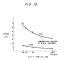
- Results of applying the waveform of either Fig. 14A or Fig. 14B are shown in Fig. 15.
- Drive conditions in this case were a reset voltage of 20 V, a reset time of 1 ms, and a delay time of 150 to 200 us.
- the duty ratio of application pulse width t with respect to selection period T3 is plotted along the X-axis. Peak voltage when the application pulse is on (0 uniform orientation state) or off (360 twist orientation state) is plotted along the Y-axis.
- the pulse duty ratio of the applied voltage is reduced from 50% to 33% and then to 25%, the peak voltage rises by root two, root three, and two. Therefore, this embodiment has the characteristic that the RMS value calculated within selection period T3 is always uniform.
- the ratio of the ON voltage to the OFF voltage is one characteristic that does not change, no matter how the duty ratio changes. The ratio is approximately five for the liquid crystal used for the measurement of Fig. 15.
- Figs. 16A to 16E show matrix drive waveforms relating to a sixth embodiment that applies the drive waveform of Fig. 14B to the alternating drive of a matrix display.
- Yn, Yn + 1, Yn + 2 indicate the scan signals supplied to the nth, (n + 1)th, and (n + 2)th row electrodes, respectively.
- Xm indicates the data signal supplied to the mth column electrode.
- the duty ratio of the total period t of the data potential of this data signal Xm with respect to selection period T3 is set to less than 100%, in the same manner as with the scan signal.
- the difference signal Yn-Xm between the scan and data signals is applied to the liquid crystal.
- the duty ratio of the application period t of the ON or OFF selection voltages with respect to selection period T3 is set to be less than 100%. Therefore, both the selection voltage and the bias voltage are applied to the liquid crystal as intermittent pulses of duty ratio less than 100%.
- the inventors of the present invention have used this method to implement a simple matrix drive display using a 1/5 bias method of duty ratio 1/240 under the following conditions: a reset voltage of ⁇ 25 V, a reset period of 1 ms, a delay period of 200 us, a selection period of 100 us, a pulse selection time of 25 /1.s x 2 (duty ratio 50%), a selection voltage of ⁇ 4 V, and a data voltage of ⁇ 1 V.
- the frame frequency was 42 Hz and no flickering was generated.
- Figs. 17A-17E show another practical example of application to a matrix display of the present invention.
- scan signals Yn, Yn + 1, and Yn + 2 each have the same waveforms as the corresponding waveforms in Fig. 16.
- Data signal Xm shown in Fig. 17 differs from the corresponding one of Fig. 16 in that the duty ratio of the pulse width of the data potential with respect to selection period T3 is set to 100%.
- the voltage of difference signal Yn-Xm is applied to the liquid crystal, but, with this difference signal Yn-Xm, the duty ratio of the application period t of the ON or OFF selection voltages with respect to selection period T3 is set to less than 100%.
- the bias voltage is applied to the liquid crystal without interruptions, and the selection pulse has a pulse duty ratio of less than 100%.
- This method has been used to implement a simple matrix drive display using a 1/5 bias method of duty ratio 1/240 under the following conditions at an ambient temperature of 40 °C: a reset voltage of ⁇ 25 V, a reset period of 1 ms, a delay period of a 200 us, a selection period of 100 us, a pulse selection time of 50 /1.s x 2 (duty ratio 100%), a selection voltage of ⁇ 4 V, and a data voltage of ⁇ 1 V.
- the frame frequency was 42 Hz and no flickering was generated.
- FIG. 19A to 19E A further example of the application of the present invention to a matrix display is shown in Figs. 19A to 19E.
- the duty ratio of the pulse width of the ON selection potential or OFF selection potential with respect to selection period T3 is set to 100%.
- the duty ratio of the pulse width t of the data potential of the data signal Xm with respect to selection period T3 is set to less than 100%.
- the resultant difference signal Yn-Xm is applied to the liquid crystal, and, in this difference signal Yn-Xm too, the duty ratio of the application period t of the ON or OFF selection voltages with respect to selection period T3 is set to less than 100%.
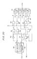
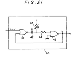
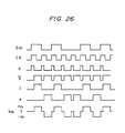
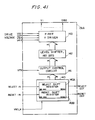
- Fig. 20 shows a circuit that outputs a scan signal Yn having the various potentials shown in Fig. 22, based on a clock signal CLK, a reset signal RE, and a select signal S.
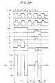
- Fig. 22 shows scan signal Yn has potentials of ⁇ V2 during reset period T1, potentials of ⁇ V1 as selection pulses during selection period T3, and a potential of 0 V in all other periods.
- a monostable circuit 40, a 1/2 divider 46, and various logic gates 50-55 and 60-64 are used to drive these analog switches 70-74 in a switching manner.
- Monostable circuit 40 receives as inputs the reference clock CLK and generates a signal _b_ that is high for a period of time proportional to a time constant CR of its circuitry.
- Monostable circuit 40 has, as shown in Fig. 21, a first NOR circuit 41, a capacitor 42, a variable resistor 43, a resistor 44, and a second NOR circuit 45.
- the time constant of monostable circuit 40 is determined by the capacitance C of capacitor 42 and the resistance R of variable resistor 43, so that it is possible to vary the duty ratio of the pulse width of the selection pulse with respect with selection period T3 of scan signal Yn by varying the resistance R of variable resistor 43, as described below.
- the 1/2 divider 46 receives as inputs the reference clock CLK and generates a signal _a_ of half the frequency of the reference clock CLK, or rather of twice the period thereof.
- a first AND circuit 52 receives as inputs signals that are the above described signals a and _b_ after being inverted by first and second inverters 50, 51, and generates a signal _d_ shown in Fig. 22.
- a third AND circuit 54 receives as inputs the signal _d_ and the select signal S, and generates a signal _e_ that switches over first analog switch 70.
- Signal _e_ is high throughout a period corresponding to the pulse width of the selection pulse when it has negative polarity within selection period T3 of scan signal Yn, as shown in Fig. 22.
- a second AND circuit 53 receives as inputs the signal _a_ and a signal that is the signal _b_ after being inverted by second inverter 51, and generates a signal _c_ shown in Fig. 22.
- a fourth AND circuit 55 receives as inputs the signal _c and select signal S, and generates a signal _f_ for switching second analog switch 71.
- Signal _f_ is high throughout a period corresponding to the pulse width of the selection pulse when it has positive polarity within selection period T3 of scan signal Yn, as shown in Fig. 22.
- Signals _e_ and _f_ used to drive first and second analog switches 70, 71 determine the duty ratio of the pulse width of the selection pulse with respect to selection period T3 of scan signal Yn.
- the pulse width of each of these signals _e_ and _f_ is determined based on the signal _b_ from monostable circuit 40, and thus it is clear that, by varying the time constant CR of monostable circuit 40, the duty ratio of the pulse width of the selection pulse with respect to selection period T3 of scan signal Yn can be varied.
- Signals _g_ to _i_ that drive third to fifth analog switches 72 to 74 to switch the potential of the scan signal outside of the selection pulse are now described.
- Signal _g_ that is used to switch over third analog switch 72 is generated by a fifth AND circuit 60 that receives as inputs the signal _a_ and reset signal RE.
- Signal _g_ is high throughout periods corresponding to periods during which the reset potential has positive polarity at +V2 within reset period T1 of scan signal Yn, as shown in Fig. 22.
- Signal _ h _ that is used to switch over fourth analog switch 73 is generated by a sixth AND circuit 61 that receives as inputs reset signal RE and a signal that is the signal _a_ after being inverted by first inverter 50.
- Signal _h_ is high throughout periods corresponding to periods during which the reset potential has negative polarity at -V2 within reset period T1 of scan signal Yn, as shown in Fig. 22.
- Signal _i_ that is used to switch fifth analog switch 74 is generated by sixth AND circuit 61, a seventh AND circuit 62, a third NOR circuit 63, and an OR circuit 64, based on signal _b_, reset signal RE, and select signal S.
- Signal _i_ is high throughout periods corresponding to periods of scan signal Yn during which the selection pulse is not output within delay period T2, nonselection period T4, and selection period T3, as shown in Fig. 22.
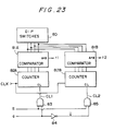
- the tenth embodiment of the present invention differs in that the varying of the duty ratio is done in a digital manner from the ninth embodiment in which the duty ratio is changed in a continuous manner by varying the resistance R.
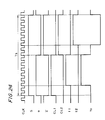
- a block diagram of a circuit that outputs signals t1 and t2 used for determining the pulse width of positive and negative selection pulses within selection period T3 of scan signal Yn is shown in Fig. 23, and a timing chart of this circuit is shown in Fig. 24.
- DIP switches 80, first and second magnitude comparators 81A, 81B, and first and second counters 82A, 82B are provided as the circuitry that generates signals t1 and t2.
- the pulse width that makes signals t1 and t2 high is set, e.g., by binary DIP switches 80.
- DIP switches 80 are connected to first and second magnitude comparators 81A, 81 B which could, be 4-bit comparators.
- First and second counters 82A, 82B count reference clock CLK, as shown in Fig. 24.
- Signals CL1 and CL2 shown in Fig. 24 are input to clear pins CL of first and second counters 82A, 82B.
- Signal CL1 is output from an AND circuit 83 that receives as inputs select signal S and signal _a_.
- Signal CL2 is output by an AND circuit 85 that receives as inputs select signal S and a signal that is the signal _a_ after being inverted by an inverter 84.
- first and second counters 82A, 82B are designed to be cleared by signals CL1 and CL2 going high.
- An eleventh embodiment of the present invention is designed to vary the duty ratio of the period of the ON potential or OFF potential with respect to selection period T3 of the data signal Xm.
- a data signal drive circuit 90 for outputting the data signal Xm supplied to the column electrode of the mth column is shown in Fig. 25, and a timing chart of this circuit is shown in Fig. 26.
- This data signal drive circuit 90 has a sixth analog switch 94 for outputting a potential -V3 as the data signal Xm, a seventh analog switch 95 for outputting a potential V3, and an eighth analog switch 96 for outputting a potential 0.
- Analog switches 94-96 are provided with logic gates 91-93 for providing switching drive.
- An eighth AND circuit 91 is provided for switching seventh analog switch 95.
- Eighth AND circuit 91 receives data Dm for the mth column and a signal that is the signal _b_ from monostable circuit 40 of Fig. 20, after it has been inverted by the second inverter 51.
- an output signal - j - of eighth AND circuit 91 is high throughout a period corresponding to the width of a pulse that has a potential of +V3, during selection period T3 corresponding to one horizontal scanning period of the data signal Xm.
- a ninth AND circuit 93 is provided for switching first analog switch 94.
- Ninth AND circuit 93 receives a signal that is the data Dm after being inverted by a third inverter 92 and the signal that is the signal _b_ after it has been inverted by second inverter 51, and generates a signal _k_.
- Signal k is high throughout a period corresponding to the width of a pulse that has a potential of -V3, during selection period T3 of the data signal Xm, as shown in Fig. 26.
- Eighth analog switch 96 is switched by signal _b_ from monostable circuit 40. In this way, the duty ratio of the data potential with respect to the selection period of the data signal Xm can be varied based the time constant CR of monostable circuit 40.
- the means of varying the duty ratio of the data potential period with respect to the selection period of data signal Xm could be done in a digital manner, in the same way as in embodiment ten.
- Fig. 27 shows a block diagram of a matrix liquid crystal display device that can vary the duty ratio of the selection pulse width with respect to selection period T3.
- the data necessary for the display is stored temporarily in a memory 100, then is transferred through a display controller 101 to an X driver 102 and a Y driver 103.
- a duty ratio controller 107 that causes a change in the pulse width duty ratio of X driver 102 or Y driver 103 in accordance with a signal from a temperature sensor 104 or a manual switch 106, so that the duty ratio of the pulses from the X driver or Y driver are determined either automatically or manually by this setting.
- This setting could be the continuous variation of the ninth and eleventh embodiments or the stepwise variation of the tenth embodiment.
- the pulse train applied to liquid crystal panel 108 can be adjusted in correspondence with the ambient temperature, and is a waveform optimized for ease of viewing.
- duty ratio controller 107 to display controller 101 enables either continuous or stepwise variation of the pulses applied to the liquid crystal during selection period T3, so that the RMS voltages of the pulse applied to the liquid crystal can be varied thereby.
- This of course means that irregularities in drive voltage between individual liquid crystal panels are absorbed, and changes in drive voltage due to variations in ambient temperature can be adjusted for without changing the power supply voltage.
- the configuration is such that the user of the liquid crystal display panel can apply direct adjustment by an external operating switch, the display can be adjusted to the user's own optimal state. If it is found during circuit fabrication that the difference between the reset voltage and the data voltage is large and thus it is difficult to provide an accurate power supply voltage, this problem can be solved by lowering the pulse duty ratio and raising the peak value. With a color display, the pulse duty ratio could be adjusted for each of the RGB drive voltages, even if there are differences in cell gap or threshold value due to difference in RGB filter thickness.
- At least one of the scan signals (row electrode signals) supplied to a plurality of row electrodes can be set such that the duty ratio of the period of the selection potential with respect to the selection period has a different value from that of the other row electrode signals. For example, varying the above described duty ratio for the row electrodes at the upper and lower parts of the liquid crystal panel can compensate for irregularities in the threshold value of the liquid crystal at the upper and lower parts of the liquid crystal panel. Similarly, at least one of the data signals (column electrode signals) supplied to a plurality of column electrodes can be set such that the duty ratio of the data potential period with respect to the selection period has a different value from that of the other column electrode signals.
- varying the above described duty ratio for the column electrodes at the left and right of the liquid crystal panel can compensate for irregularities in the threshold value of the liquid crystal at the left and right sides of the liquid crystal panel.
- an individual column electrode signal supplied to the column electrode of one column could be observed, and the column electrode signal could be adjusted such that the duty ratio of the period of the data potential with respect to the selection period corresponding to one pixel on one of the column electrodes that is supplied with one of the column electrode signals is set to be different from that of the selection periods corresponding to the other pixels on that column electrode. This can compensate for differences in drive voltage at the top and bottom of the liquid crystal screen attributed to irregularities in the threshold value at each pixel.
- the above described drive method that modifies the duty ratio can be applied in the same way to a drive method in which no delay period is provided, such as that shown in Fig. 3 or Fig. 13.
- Embodiments nine through twelve compensated for irregularities in the threshold value of the liquid crystal medium making up the liquid crystal panel or irregularities in the threshold value caused by ambient temperature by varying the duty ratio of the period of the selection pulse with respect to the selection period, but any of the several parameters described below can be varied to change the threshold value of the liquid crystal.
- the pulse height of the selection pulse could be varied to suit the threshold value of the liquid crystal.
- Further examples of parameters that could be used to vary the threshold value of the liquid crystal are the width of the selection pulse and the length of delay period T2 that sets the timing for applying the selection pulse.
- the critical value is the heights of the selection pulses, which are shown by Vth1 and Vth2 in Fig. 28.
- a1 and a2 represent regions in which one of the metastable states (e.g., the state in which the angle of twist is zero) occurs (_ Ve _ > VO and _ Vth1 _ ⁇ _ Vs _ ⁇ _ Vth2 _).
- b1, b2, and b3 represent regions in which the other of the metastable states (e.g., the state in which the angle of twist is 360°) occurs ( _ Ve _ > VO and_ Vs _ ⁇ _ Vth1 _, or _ Ve _ > VO and_ Vs _ > _ Vth2 _ ).
- Vth1 and Vth2 are threshold values with respect to the selection pulse voltage, and in actual practice there can be three or more of these threshold values.
- Vth1 acts as threshold value for driving the liquid crystal.
- a critical value could be obtained from a combination of the above three parameters.
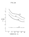
- a negative correlation between temperature T and threshold values Vth and Vsat is shown in Fig. 29
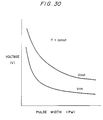
- a negative correlation between pulse width Pw and threshold values Vth and Vsat is shown in Fig. 30
- a correlation between delay time t and threshold values Vth and Vsat is shown in Fig. 31.
- the thirteenth to fifteenth embodiments described below relate to temperature compensation implemented by changing one of the above described parameters, using temperature sensor 21 and temperature compensation circuit 22 of Fig. 5.
- Temperature sensor 21 measures the ambient temperature of liquid crystal cell 11 and sends a corresponding measurement signal to temperature compensation circuit 22.
- Temperature compensation circuit 22 outputs a compensation control signal _x_ or _y_ to potential setting circuit 17 or line sequential scan circuit 18, to correspond to one of a plurality of temperature compensation methods described below. This is designed to modify the output potential of potential setting circuit 17 or change control frequency or control pattern of the line sequential scan circuit.
- a working temperature region could be divided into a plurality of temperature ranges, one of the above parameters could be preset to have a different value within each of these temperature ranges, and temperature compensation could be provided by selecting a setting for the parameter in the temperature range that the ambient temperature belongs to.
- the drive waveform that drives the simple matrix type of liquid crystal display panel shown in Fig. 5 could be that shown in either Fig. 2A or Fig. 2B.
- the drive waveform shown in Fig. 3 that applies the selection pulse immediately after the reset period has elapsed could be used.
- a thirteenth embodiment of the present invention provides optimal liquid crystal drive that is tailored to the threshold value of the liquid crystal, by changing the pulse height of the selection pulse.
- the duty ratio of selection period T3 with respect to one frame period T was set to 1/240, the pulse width (length of the selection period T2) to 40 us, delay period T2 to 200 us, and the signal potential Vd to ⁇ 1.2 V.
- Changes with respect to temperature of threshold values Vth and Vsat when an ON state (corresponding to a uniform orientation state where the angle of twist is zero) and an OFF state (corresponding to a twist orientation state where the angle of twist is 360°) were obtained were investigated in a normal temperature region within the range of 0°C to 50 °C.
- This adjustment of the scan potential Vw adjusted the setting potential of potential setting circuit 17 by an output signal from temperature compensation circuit 22, in other words, the drive voltage.
- the absolute value of the selection voltage could be set to be large if the threshold value of the liquid crystal is high, or small if the threshold value of the liquid crystal is low.
- a fourteenth embodiment of the present invention implements temperature compensation by using the output signal from temperature compensation circuit 22 to adjust the control frequency of line sequential scan circuit 18 (i.e., the drive frequency of the liquid crystal display panel) in a stepwise fashion.
- the duty ratio of selection period T3 with respect to one frame period T was set to 1/240, the signal potential Vd to ⁇ 1.2 V, and the potential Vw of the scan signal in the selection period to ⁇ 4.2 V.
- the adjustment method was such that, in the temperature region 15 to 35 °C, pulse width Pw was 40 us and the delay time t was 200 us.
- the drive frequency could be set to be low or selection period T3 long when the threshold value of the liquid crystal is high; or the drive frequency could be set to be low or selection period T3 short when the threshold value of the liquid crystal is low.
- a fifteenth embodiment of the present invention implements temperature compensation by using the output signal from temperature compensation circuit 22 to adjust the control pattern of line sequential scan circuit 18 in a stepwise fashion, to adjust the length of delay period T2.
- the duty ratio of selection period T3 with respect to one frame period T was set to 1/240, signal potential Vd to ⁇ 1.2 V, potential Vw of the scan signal in selection period T3 to ⁇ 4.2 V, and pulse width Pw of the selection pulse to 40 us.
- delay period T2 can be set to be long when the threshold value of the liquid crystal is high; or short when the threshold value of the liquid crystal is low.
- TP indicates the type of drive waveform, where type 1 is the drive waveform shown in Fig. 3, both type 2 and type 4 are the drive waveform shown in Fig. 2A, and both type 3 and type 5 are the drive waveform shown in Fig. 2B.
- Adjustment of the delay time t corresponding to delay period T2 enables a shortening of the pulse width Pw while controlling the ON voltage, and can thus shorten the write time, so that the number of scan lines can be increased.
- a chiral nematic liquid crystal having characteristics superior to those of STN liquid crystal, such as a memory capability (of 1 second, roughly) in metastable states, a high contrast ratio (of at least 100), wide viewing angle (of 60 to 800), and rapid response (of 8 ms or less), will be extremely effective in producing the kinds of 640 x 400 and 640 x 480 pixel matrix display panel that are in such demand, without seeking the help of active elements.
- critical values used as reference when either of two metastable states are selected were determined from the three parameters of voltage value, pulse width, and delay time that indicate the imposed state of the selection pulse, and stable liquid crystal display can be implemented by adjusting them so that changes in the critical value due to temperature variations can be compensated for.
- temperature compensation within the working temperature region can be controlled by controlling any one of the above described three parameters, these embodiments are extremely significant in that they ensure a large degree of freedom over drive conditions.
- the present invention enables the stable drive of a display panel with a simple circuit configuration by adjusting the drive voltage or drive frequency.
- a temperature sensor is provided in the circuit to provide automatic temperature compensation, voltage or frequency could be adjusted in an analog fashion in accordance with a detection signal from the temperature sensor, but the resultant circuit configuration would be complicated.
- a simple form of temperature compensation could be enabled by having a selection circuit select and switch the drive voltage in a digital fashion, or by having a switching circuit switch the drive clock in a digital fashion.
- This type of temperature compensation is not limited to being based automatically on the output of a temperature sensor; a manual operation by a manual switch could also be performed instead.
- the present invention is not necessarily limited to the above described temperature compensation based on the variation of aforementioned parameters; it can also be used to compensate for the irregularities in the threshold value of the liquid crystal shown in Fig. 49.
- Fig. 8 shows a drive waveform using seven voltage levels that are voltage levels of the scan and data signals.
- the voltage level Vr of scan signal Yn in reset period T1 must exceed 20 V.
- a voltage in the vicinity of 1 V is sufficient as the voltage level Vb of the data signal Yn. Therefore, with the drive waveform shown in Fig. 8, a large potential difference is created between scan signal Yn and the data signal Xm. Further, even within the same scan signal Yn waveform, a voltage difference in the vicinity of 20 V is created between the voltage Vr and the voltage 2Vb.
- a six-level drive method has been proposed as a voltage-averaging drive method for a matrix liquid crystal display device (refer to p. 401 of the Liquid Crystal Device Handbook, published by Nikkan Kogyo Shimbun, Ltd.).
- This six-level drive method is effective in balancing the drive voltages of the waveforms of the scan and data signals, and making the ratio of the ON voltage to the bias voltage large.
- a reset voltage of a comparatively large value is necessary to drive the liquid crystal that is the target of the present invention, so this six-level drive method is unable to solve the above described problem.
- delay period T2 is provided between reset period T1 and selection period T3 of the scan signal, but the eight-level drive method can also be applied to drive methods in which this delay period T2 is not provided, such as that shown in Fig. 3 or Fig. 13.
- Scan signals Yn and Yn + 1 indicate the scan signals supplied to the nth and the (n + 1)th row electrodes, respectively.
- Eight levels of potential that set these scan and data signals are provided: four levels in a first, low-voltage group (V1, V2, V3, and V4, where V1 ⁇ V2 ⁇ V3 ⁇ V4) and four levels in a second, high-voltage group (V5, V6, V7, and V8, where V4 ⁇ V5 ⁇ V6 ⁇ V7 ⁇ V8).
- the data signal Yn for the kth frame (where k is an integer) is set to voltage V1 during reset period T1, voltage V6 during delay period T2, voltage V8 during selection period T3, and voltage V6 during nonselection period T4.
- the equivalent levels are symmetrical with those of the kth frame about a voltage midway between V4 and V5.
- scan signal Yn for the (k + 1)th frame is set to voltage V8 during reset period T1, voltage V3 during delay period T2, voltage V1 during selection period T3, and voltage V3 during nonselection period T4.
- the subsequent (k + 2)th frame has the same waveform as that of the kth frame, and the waveform repeats the same relationship thereafter.
- Scan signal Yn + 1 is the waveform of the next row's scan signal. It differs from scan signal Yn in that each of reset period T1, delay period T2, and selection period T3 are shifted by the time (1 H) required for one line. The beginning and end of the first frame are at the same point as in scan signal Yn, but the waveform of the scan signal is shifted by 1 H otherwise.
- the ON voltage on the display of the data signal Xm is set to either V4 or V5, and the OFF voltage to either V2 or V7.
- V5 on the high-potential side is ON and V7 is OFF, to ensure that the largest potential difference with the reset voltage V1 is achieved.
- the phases of the waveforms of the scan and data signals are in a 180 ° shifted relationship.
- V4 on the low-potential side is ON and V2 is OFF, which ensures that the maximum potential difference with the reset voltage V8 is generated.
- the voltages can be set further apart in the positive and negative directions, so as to make the potential difference between the voltage V4 of the first group and the voltage V5 of the second group even wider, so that a reset voltage of 30 V or 40 V with a bias voltage of 1 V can be implemented.
- Scan signal Yn in Fig. 33 is at voltage V1 (frame k) or voltage V8 (frame k + 1) during reset period T1, voltage V7 (frame k) or voltage V2 (frame k + 1) during delay period T2, voltage V5 (frame k) or voltage V4 (frame k + 1) during selection period T3, and the voltage V7 (frame k) or voltage V2 (frame k + 1) during nonselection period T4.
- This scan signal Yn is symmetrical about an axis at an intermediate point between the voltages V4 and V5, and inverts every frame.
- the ON voltage of the data signal Xm is V8 and the OFF voltage is V6; in frame k + 1, the ON voltage is V1 and the OFF voltage is V3.
- the reset voltage becomes ⁇ 26 V and the other voltage amplitudes can be expanded by ⁇ 1 V over those of the sixteenth embodiment.
- the ON voltage, OFF voltage, and bias voltage are the same as those of the sixteenth embodiment.
- Fig. 34 The drive waveform of an eighteenth embodiment of the present invention that inverts the polarity of the voltage applied to the liquid crystal at each pulse is shown in Fig. 34.
- scan signal Yn is set to repeatedly alternate between two types of potential, voltages V1 and V8, every 1 H/2 (where 1 H is the length of selection period T3) during reset period T1.
- scan signal Yn is set to repeatedly alternate between two types of potential, voltages V3 and V6, every 1 H/2 during delay period T2.
- the pulses are 180 ° out of phase in comparison with the reset pulses.
- Scan signal Yn is again set to repeatedly alternate between two types of potential, voltages V1 and V8, every 1 H/2 during selection period T3. Finally, it is set to alternate repeatedly between two types of potential, voltages V3 and V6, every 1 H/2 during nonselection period T4. Similarly, data signal Xm is set to repeatedly alternate between two types of potential, voltages V4 and V5, every 1 H/2 as the ON voltage, and between two types of potential, voltages V2 and V7, every 1 H/2 as the OFF voltage.
- the drive waveform of a nineteenth embodiment that inverts the polarity of the voltage applied to the liquid crystal at each pulse, in the same manner as in the eighteenth embodiment, is shown in Fig. 35.
- Scan signal Yn in this figure differs from that of Fig. 34 in the potentials set during delay period T2, selection period T3, and nonselection period T4.
- Scan signal Yn shown in Fig. 35 is set to repeatedly alternate between two types of potential, voltages V2 and V7, every 1 H/2 during delay period T2 and nonselection period T4.
- scan signal Yn is set to repeatedly alternate between two types of potential, voltages V4 and V5, every 1 H/2 during selection period T3.
- this data signal Xm is completely different from that of the eighteenth embodiment in that the ON voltage thereof has two types of potential, voltages V1 and V8, and the OFF voltage thereof also has two types of potential, voltages V3 and V6.
- the resultant difference signal Yn-Xm between scan signal Yn and data signal Xm is designed to apply voltages of the same absolute value as those of the difference signal of the eighteenth embodiment during delay period T2, selection period T3, and nonselection period T4.
- the maximum amplitude of the difference signal Yn-Xm of the nineteenth embodiment is either V1 - V8 or V8 - V1 during reset period T1
- the amplitude of the reset voltage can be made even larger than that of the eighteenth embodiment.
- this drive method is superior to the drive method of the eighteenth embodiment.
- a twentieth embodiment of the present invention provides a method that controls the pulse drive frequency to reduce the number of inversions within one frame to approximately half that of the eighteenth embodiment.
- a signal FR that determines the timing of the pulse inversions of the scan and data signals turns on and off in every 1 H.
- the phase of this FR signal is shifted by 1 H/2 from the rise of selection period T3.
- the pulse inversion of the waveforms of scan signal Yn and the data signal Xm are in synchronization with signal FR, the number of pulse inversions within one frame is half that of the waveform shown in Fig. 34.
- the waveform of this difference signal Yn-Xm undergoes a pulse inversion every 1 H/2, in the same manner as the eighteenth embodiment, and this can ensure a long lifetime for the liquid crystal.
- the drive frequency for each driver for the scan and data signals can be halved, making it easier to shape the waveform and reducing power consumption. This is particularly advantageous for the circuitry that causes the power supply voltage required for the alternation to swing between positive and negative.
- the voltage settings in each of the periods T1 to T4 of the scan and data signals were made the same as in the eighteenth embodiment, but they can equally well be the same as in the nineteenth embodiment.
- FIG. 37 A drive method in which the pulse inversion is performed every 1 H is shown in Fig. 37.
- the FR signal is similar to that of the twentieth embodiment shown in Fig. 36 in that it turns on and off every 1 H, but differs from the twentieth embodiment in that this FR signal is in synchronism with selection period T3.
- scan signal Yn is set to voltage V1 in frame k and voltage V8 in frame (k + 1), and thus the voltages V1 and V8 alternate every frame.
- the waveform of the data signal Xm has voltage V4 as the ON voltage and voltage V2 as the OFF voltage.
- the waveform of the data signal Xm has voltage V5 as the ON voltage and voltage V7 as the OFF voltage. If the resultant difference signal Yn-Xm between the scan and data signals is observed in frame k, it is clear that a voltage of negative polarity is applied to the liquid crystal a large number of times, and thus the polarity of the voltages applied to each pixel within any one frame cannot be balanced. However, in the next frame (k + 1), the number of times a voltage of a positive polarity is applied to the liquid crystal is increased, so that the polarity of the voltages applied to the liquid crystal can be balanced over a sequence of two frames.
- the twenty-first embodiment combines the frame inversion of the sixteenth and seventeenth embodiments with the pulse inversion of the eighteenth and nineteenth embodiments.
- the advantage of this twenty-first embodiment lies in the way in which selection period T3 (1 H) can be lengthened even when driving a liquid crystal display apparatus with high duty ratio, so that the length of time that the direct-current portion of the voltage is applied to the liquid crystal can be set to be shorter than in embodiments that employ frame inversion alone.
- the voltage of each of the periods T1 to T4 of the scan and data signals of this twenty-first embodiment are set to be the same as those in the seventeenth embodiment, but they can be set to be the same as those in the eighteenth embodiment instead.
- FIG. 38 A block diagram of a drive circuit for scan signal electrodes (row electrodes), for implementing the drive methods of the sixteenth to the twenty-first embodiments, is shown in Fig. 38.
- a logic circuit 110 generates a reset signal RE that specifies reset period T1 and a select signal S that specifies selection period T3 after delay period T2 has elapsed after reset period T1, based on information on delay period T2.
- Signals RE and S are input to shift registers 111 and 112, respectively.
- Each of these registers 111 and 112 transfer signals RE and S in accordance with a shift clock SCK, and at the same time the internal states of the registers are simultaneously output in parallel to 160 channels.
- Y driver 115 receives three voltages from a power supply circuit 116 and a phase converter 117. If the power supply voltage of power supply circuit 116 acts as the alternation signal FR, each of the voltages can be made to swing ⁇ Va or ⁇ Vb.
- FIG. 39 A block diagram of the drive circuit for the data signal electrodes (column electrodes) is shown in Fig. 39.
- 8-bit image data DO to D7 is input to a data latch circuit 121 through a multiplexer 120, and it is converted into 160 channels of parallel data in the data latch circuit 121.
- the latch timing of the data latch circuit 121 is determined by latch pulses output by a control circuit 122 to which the clock SCK is input.
- the 160 channels of image data are sent from data latch circuit 121 to a level shifter 123, and at the same time an inversion operation is added by a signal from a logic circuit 125, based on the alternation signal FR.
- An X driver 124 to which these four states for each of the channels are input selects one level from power supply voltages VL1 to VL4 in accordance with the state of each channel, and outputs it.
- VL1 V7
- VL2 V2
- VL3 V5
- VL V4
- a waveform that is the same as data signal Xm of Fig. 37 which shows the drive waveform of the twenty-first embodiment, can be generated.
- a liquid crystal panel 130 has a 320 x 320-pixel structure, and first and second Y driver circuits 131A and 131B and first and second X drivers 132A and 132B are provided in order to drive this liquid crystal panel 130.
- First and second Y driver circuits 131A and 131B each have the same configuration, which is shown in Fig. 41.
- X driver circuits 132A and 132B have the same configuration, which is shown in Fig. 42.
- Y driver circuit 131A has a shift register 140 that comprises a select shift register 140A and a reset shift register 140B.
- Select shift register 140A has registers SR1 to SR160 and reset shift register 140B has registers RR1 to RR160.
- Select signal S that specifies selection period T3, is input to select shift register 140A and is sequentially shifted by shift clock YSCL in the next-stage register.
- the contents of register SR160 are output from a select out pin, enabling a cascade connection with second Y driver circuit 131 B.
- Reset signal RE which specifies reset period T1, is input to reset shift register 140B and is sequentially shifted by shift clock YSCL in the next-stage shift register.
- the contents of register RR160 are output through the reset out pin, enabling a cascade connection with second Y driver circuit 131 B.
- All 160 channels of the contents of each of shift registers 140A and 140B are input to output control circuit 141.
- V1Y, V2Y, V3Y, and V4Y are input to Y driver 143, and one drive voltage is output to each of the channels in accordance with the logical chart of Table 7, based on the six states identified and output by output control circuit 141.
- Fig. 43 The states of the input and output signals to and from the various components of first and second Y driver circuits 131A and 131B are shown in Fig. 43.
- Fig 43 if the length of selection period T3 is taken to be 1 H, a signal YFR is repeatedly turned on and off every 1 H and the polarity of the voltage applied to the liquid crystal inverts every 1 H. Since each row has 320 pixels, the duty ratio is 1/320, and reset period T1 is set to 5H and delay period T2 to 2H.
- the signal waveform of the nth scan signal Yn output by the operation of this drive circuit is shown in Fig. 45.
- First X driver circuit 132A is described with reference to Fig. 42.
- First X driver circuit 132A has a shift register 150 that has 160 registers, and data is sequentially shifted in a next-stage register in accordance with an input signal EI and a shift clock XSCL.
- the contents of the 160th register are output to the outside through an EO pin, enabling a cascade connection with second X driver circuit 132B.
- Signal EI input to shift register 150 is at a logical one once every period 1 H, as shown in Fig. 44. Therefore, a logical one is output in sequence from each register of shift register 150, and this causes a first latch circuit 151 to latch image data at addresses corresponding to its registers.
- the 160 channels of data of first latch circuit 151 is latched in a second latch circuit 152 at the timing at which a latch pulse LP is input.
- X driver 155 receives four types of drive voltage V1X, V2X, V3X, and V4X, and outputs one of the four types of drive voltage to each channel in accordance with the logical chart of Table 8, based on information from output control circuit 153.
- This difference signal inverts the voltage applied to the liquid crystal every 1 H, in the same manner as in the difference signal of Fig. 37 which shows the drive waveforms of the twenty-first embodiment. Since the voltage applied to the liquid crystal within one frame cannot be balanced between positive and negative, a balance between positive and negative in the voltage applied to the liquid crystal is achieved in the (k + 1)-th frame subsequent to the kth frame. This means that the difference signal shown in Fig. 45 combines a polarity inversion every 1 H and a polarity inversion every frame, as in the twenty-first embodiment.
- the twenty-third embodiment is more advantageous than the twenty-second embodiment from a circuit configuration viewpoint, in that switching of the voltages of each of the scan and data signals is performed by logic means.
- a drive method that enables modification of delay period T2 within the signal, using the drive circuit shown for the twenty-third embodiment, is described with reference to Figs. 46-47.
- the means of changing delay period T2 must not only change the delay period without affecting the specified position of selection period T3 within one frame T, it must also change reset period T1 before delay period T2.
- reset period T1 is set to 5H and delay period T2 to 2H
- a combination reset plus delay signal having a pulse width that is the sum of the pulse widths of reset period T1 and delay period T2 (7H) is generated before selection period T3.
- the reset signal input to reset shift register 140B of Y driver circuits 131A and 131 B can be shaped by an exclusive OR of this reset plus delay signal and the delay signal that specifies the delay period.
- delay period T2 if it becomes necessary to change delay period T2 to compensate for irregularities of the threshold value of the liquid crystal at individual pixels making up the liquid crystal panel, or for variations in the threshold value of the liquid crystal caused by ambient temperature, the specifications of delay period T2 and reset period T1 before it can be changed by the above means.
- a reset signal having the same 5H reset period T1 of Fig. 46 could be shaped by an exclusive OR of the thus modified delay signal and the reset plus delay signal.
- the method of the present invention to be described in the foregoing embodiments is suitable for driving a liquid crystal display device such as a TV, the display of a personal computer, a projector, a head mounted display, the viewfinder of a video camera, or a printer having a liquid crystal shutter.
- a liquid crystal display device such as a TV, the display of a personal computer, a projector, a head mounted display, the viewfinder of a video camera, or a printer having a liquid crystal shutter.
Landscapes
- Engineering & Computer Science (AREA)
- Physics & Mathematics (AREA)
- General Physics & Mathematics (AREA)
- Chemical & Material Sciences (AREA)
- Crystallography & Structural Chemistry (AREA)
- Theoretical Computer Science (AREA)
- Computer Hardware Design (AREA)
- Nonlinear Science (AREA)
- Optics & Photonics (AREA)
- Mathematical Physics (AREA)
- Liquid Crystal Display Device Control (AREA)
- Liquid Crystal (AREA)
- Control Of Indicators Other Than Cathode Ray Tubes (AREA)
Priority Applications (1)
| Application Number | Priority Date | Filing Date | Title |
|---|---|---|---|
| EP98110226A EP0866441B1 (de) | 1993-02-25 | 1994-02-24 | Steuerungsverfahren für Flüssigkristallanzeigeeinrichtung mit 8 Spannungspegeln |
Applications Claiming Priority (18)
| Application Number | Priority Date | Filing Date | Title |
|---|---|---|---|
| JP37057/93 | 1993-02-25 | ||
| JP3705793 | 1993-02-25 | ||
| JP3705793 | 1993-02-25 | ||
| JP12170693 | 1993-05-24 | ||
| JP12170693 | 1993-05-24 | ||
| JP121706/93 | 1993-05-24 | ||
| JP198604/93 | 1993-08-10 | ||
| JP19860493 | 1993-08-10 | ||
| JP19860493 | 1993-08-10 | ||
| JP26389893 | 1993-10-21 | ||
| JP26389893 | 1993-10-21 | ||
| JP263898/93 | 1993-10-21 | ||
| JP27573693 | 1993-11-04 | ||
| JP27573693 | 1993-11-04 | ||
| JP275736/93 | 1993-11-04 | ||
| JP35249393 | 1993-12-29 | ||
| JP35249393A JP3489169B2 (ja) | 1993-02-25 | 1993-12-29 | 液晶表示装置の駆動方法 |
| JP352493/93 | 1993-12-29 |
Related Child Applications (1)
| Application Number | Title | Priority Date | Filing Date |
|---|---|---|---|
| EP98110226A Division EP0866441B1 (de) | 1993-02-25 | 1994-02-24 | Steuerungsverfahren für Flüssigkristallanzeigeeinrichtung mit 8 Spannungspegeln |
Publications (3)
| Publication Number | Publication Date |
|---|---|
| EP0613116A2 true EP0613116A2 (de) | 1994-08-31 |
| EP0613116A3 EP0613116A3 (en) | 1995-09-13 |
| EP0613116B1 EP0613116B1 (de) | 2000-05-10 |
Family
ID=27549841
Family Applications (2)
| Application Number | Title | Priority Date | Filing Date |
|---|---|---|---|
| EP98110226A Expired - Lifetime EP0866441B1 (de) | 1993-02-25 | 1994-02-24 | Steuerungsverfahren für Flüssigkristallanzeigeeinrichtung mit 8 Spannungspegeln |
| EP94102831A Expired - Lifetime EP0613116B1 (de) | 1993-02-25 | 1994-02-24 | Verfahren zum Steuern eines Flüssigkristallanzeigegeräts |
Family Applications Before (1)
| Application Number | Title | Priority Date | Filing Date |
|---|---|---|---|
| EP98110226A Expired - Lifetime EP0866441B1 (de) | 1993-02-25 | 1994-02-24 | Steuerungsverfahren für Flüssigkristallanzeigeeinrichtung mit 8 Spannungspegeln |
Country Status (7)
| Country | Link |
|---|---|
| US (3) | US5684503A (de) |
| EP (2) | EP0866441B1 (de) |
| JP (1) | JP3489169B2 (de) |
| KR (1) | KR100238903B1 (de) |
| DE (2) | DE69424330T2 (de) |
| HK (1) | HK1014288A1 (de) |
| SG (1) | SG72608A1 (de) |
Cited By (12)
| Publication number | Priority date | Publication date | Assignee | Title |
|---|---|---|---|---|
| EP0768557A1 (de) * | 1995-04-25 | 1997-04-16 | Citizen Watch Co. Ltd. | Verfahren und apparat zur ansteuerung einer antiferroelektrischen flüssigkristallanzeigevorrichtung |
| EP0772067A1 (de) * | 1995-05-17 | 1997-05-07 | Seiko Epson Corporation | Flüssigkristall-anzeigevorrichtung, verfahren zu ihrer ansteuerung und steuerschaltkreis sowie dafür verwendete stromversorgung |
| EP0780825A1 (de) * | 1995-12-20 | 1997-06-25 | Denso Corporation | Flüssigkristallanzeigeeinrichtung mit Matrix-Elektrodenstruktur mit reduziertem Flimmern |
| EP0911793A1 (de) * | 1997-10-22 | 1999-04-28 | Seiko Epson Corporation | Verbessertes Polaritätsumkehrungsschema für bistable nematische Flüssigkristallanzeige |
| EP0954841A4 (de) * | 1997-05-07 | 1999-11-10 | ||
| US6307533B1 (en) | 1997-08-21 | 2001-10-23 | Denso Corporation | Liquid crystal display device with matrix electrode structure |
| GB2367177A (en) * | 2000-09-23 | 2002-03-27 | Sharp Kk | Operating a bistable liquid crystal display |
| WO2005027088A1 (en) * | 2003-09-18 | 2005-03-24 | Koninklijke Philips Electronics, N.V. | An electrophoretic display with reduced look-up-table memory |
| WO2005027087A1 (en) * | 2003-09-12 | 2005-03-24 | Koninklijke Philips Electronics, N.V. | Method of compensating temperature dependence of driving schemes for electrophoretic displays |
| US7023409B2 (en) | 2001-02-09 | 2006-04-04 | Kent Displays, Incorporated | Drive schemes for gray scale bistable cholesteric reflective displays utilizing variable frequency pulses |
| CN100557676C (zh) * | 2003-09-12 | 2009-11-04 | 皇家飞利浦电子股份有限公司 | 补偿电泳显示器驱动方案的温度依赖性的方法 |
| WO2011031509A2 (en) | 2009-08-27 | 2011-03-17 | 3M Innovative Properties Company | Fast transitions of large area cholesteric displays |
Families Citing this family (101)
| Publication number | Priority date | Publication date | Assignee | Title |
|---|---|---|---|---|
| IT1271866B (it) * | 1994-02-25 | 1997-06-09 | Univ Roma | Metodo di comando di un pannello matriciale a cristallo liquido ferroelettrico. |
| JP3669708B2 (ja) * | 1995-07-03 | 2005-07-13 | シチズン時計株式会社 | 液晶表示装置 |
| US7999787B2 (en) | 1995-07-20 | 2011-08-16 | E Ink Corporation | Methods for driving electrophoretic displays using dielectrophoretic forces |
| US7193625B2 (en) * | 1999-04-30 | 2007-03-20 | E Ink Corporation | Methods for driving electro-optic displays, and apparatus for use therein |
| JP3442581B2 (ja) * | 1996-08-06 | 2003-09-02 | 株式会社ヒューネット | ネマティック液晶の駆動方法 |
| EP0863427B1 (de) | 1996-08-19 | 2001-04-18 | Seiko Epson Corporation | Verfahren zur ansteuerung einer flüssigkristall-anzeigevorrichtung |
| JP3529999B2 (ja) * | 1997-02-06 | 2004-05-24 | 株式会社リコー | 液晶セルおよびその駆動方法 |
| JP3342341B2 (ja) * | 1997-03-13 | 2002-11-05 | キヤノン株式会社 | 液晶装置及び液晶装置の駆動方法 |
| GB9717597D0 (en) * | 1997-08-21 | 1997-10-22 | Sharp Kk | Liquid crystal device |
| US20010052885A1 (en) * | 1997-09-12 | 2001-12-20 | Masaya Okita | Method for driving a nematic liquid crystal |
| EP1577874A3 (de) * | 1998-02-09 | 2006-09-13 | Seiko Epson Corporation | Elektrooptische Vorrichtung und Verfahren zu ihrer Steuerung, Flüssigkristallvorrichtung und Verfahren zu ihrer Steuerung, Treiberschaltung für elektrooptische Vorrichtung und elektronisches Gerät |
| JPH11296150A (ja) | 1998-04-10 | 1999-10-29 | Masaya Okita | 液晶の高速駆動方法 |
| EP1026658A4 (de) * | 1998-08-03 | 2005-02-09 | Seiko Epson Corp | Elektrooptische vorrichtung, substrat dafür, elektronische vorrichtung und projektionsanzeigegerät |
| US6323834B1 (en) * | 1998-10-08 | 2001-11-27 | International Business Machines Corporation | Micromechanical displays and fabrication method |
| JP2000310969A (ja) * | 1999-02-25 | 2000-11-07 | Canon Inc | 画像表示装置及び画像表示装置の駆動方法 |
| JP2000267070A (ja) * | 1999-03-18 | 2000-09-29 | Alps Electric Co Ltd | 液晶表示装置およびその駆動方法 |
| US7012600B2 (en) | 1999-04-30 | 2006-03-14 | E Ink Corporation | Methods for driving bistable electro-optic displays, and apparatus for use therein |
| US7119772B2 (en) * | 1999-04-30 | 2006-10-10 | E Ink Corporation | Methods for driving bistable electro-optic displays, and apparatus for use therein |
| US6507330B1 (en) * | 1999-09-01 | 2003-01-14 | Displaytech, Inc. | DC-balanced and non-DC-balanced drive schemes for liquid crystal devices |
| KR100641729B1 (ko) * | 1999-09-22 | 2006-11-02 | 엘지.필립스 엘시디 주식회사 | 액정표시장치의 리셋 방법 및 장치 |
| JP3618066B2 (ja) * | 1999-10-25 | 2005-02-09 | 株式会社日立製作所 | 液晶表示装置 |
| JP3606138B2 (ja) * | 1999-11-05 | 2005-01-05 | セイコーエプソン株式会社 | ドライバic、電気光学装置及び電子機器 |
| JP2001215932A (ja) * | 1999-11-22 | 2001-08-10 | Sharp Corp | 表示装置およびその駆動方法 |
| KR100734927B1 (ko) * | 1999-12-27 | 2007-07-03 | 엘지.필립스 엘시디 주식회사 | 액정표시장치 |
| WO2001056004A1 (en) * | 2000-01-31 | 2001-08-02 | Three-Five Systems, Inc. | Methods and apparatus for driving a display |
| US6812913B2 (en) * | 2000-02-17 | 2004-11-02 | Minolta Co., Ltd. | Liquid crystal display driving method and liquid crystal display device |
| JP3486599B2 (ja) * | 2000-03-31 | 2004-01-13 | キヤノン株式会社 | 液晶素子の駆動方法 |
| KR20020032439A (ko) * | 2000-04-25 | 2002-05-03 | 요트.게.아. 롤페즈 | 그레이 스케일을 얻기 위한 디스플레이 디바이스의 구동 |
| GB0010825D0 (en) * | 2000-05-04 | 2000-06-28 | Varintelligent Bvi Ltd | Matrix driving schemes for cholesteric liquid crystal displays |
| JP4706123B2 (ja) * | 2000-05-29 | 2011-06-22 | コニカミノルタホールディングス株式会社 | 液晶表示装置及び液晶表示素子の駆動方法 |
| JP4166448B2 (ja) * | 2000-10-06 | 2008-10-15 | シャープ株式会社 | アクティブマトリクス型液晶表示装置およびその駆動方法 |
| JP4258128B2 (ja) * | 2001-03-13 | 2009-04-30 | コニカミノルタホールディングス株式会社 | 液晶表示素子の駆動方法及び液晶表示装置 |
| TW574512B (en) * | 2001-03-14 | 2004-02-01 | Koninkl Philips Electronics Nv | Electrophoretic display device |
| JP3804502B2 (ja) * | 2001-09-27 | 2006-08-02 | カシオ計算機株式会社 | 液晶表示装置の駆動方法 |
| JP2003134520A (ja) * | 2001-10-19 | 2003-05-09 | Minolta Co Ltd | デジタルカメラ |
| CN102789758B (zh) * | 2001-11-20 | 2016-05-18 | 伊英克公司 | 驱动双稳态电光显示器的方法 |
| US8593396B2 (en) | 2001-11-20 | 2013-11-26 | E Ink Corporation | Methods and apparatus for driving electro-optic displays |
| US9412314B2 (en) | 2001-11-20 | 2016-08-09 | E Ink Corporation | Methods for driving electro-optic displays |
| US8558783B2 (en) | 2001-11-20 | 2013-10-15 | E Ink Corporation | Electro-optic displays with reduced remnant voltage |
| US7528822B2 (en) * | 2001-11-20 | 2009-05-05 | E Ink Corporation | Methods for driving electro-optic displays |
| US8125501B2 (en) | 2001-11-20 | 2012-02-28 | E Ink Corporation | Voltage modulated driver circuits for electro-optic displays |
| US7952557B2 (en) * | 2001-11-20 | 2011-05-31 | E Ink Corporation | Methods and apparatus for driving electro-optic displays |
| US9530363B2 (en) | 2001-11-20 | 2016-12-27 | E Ink Corporation | Methods and apparatus for driving electro-optic displays |
| JP3928438B2 (ja) * | 2001-11-30 | 2007-06-13 | コニカミノルタホールディングス株式会社 | 液晶表示素子の駆動方法、駆動装置及び液晶表示装置 |
| AU2003205965A1 (en) | 2002-03-15 | 2003-09-29 | Koninklijke Philips Electronics N.V. | Electrophoretic active matrix display device |
| JP3637911B2 (ja) * | 2002-04-24 | 2005-04-13 | セイコーエプソン株式会社 | 電子装置、電子機器、および電子装置の駆動方法 |
| JP4486319B2 (ja) * | 2002-05-09 | 2010-06-23 | 三星電子株式会社 | 階調電圧発生装置及び階調電圧発生方法及びこれを利用した反射−透過型液晶表示装置 |
| AU2003230108A1 (en) * | 2002-05-24 | 2003-12-12 | Koninklijke Philips Electronics N.V. | An electrophoretic display and a method of driving an electrophoretic display |
| US20080024482A1 (en) | 2002-06-13 | 2008-01-31 | E Ink Corporation | Methods for driving electro-optic displays |
| US20110199671A1 (en) * | 2002-06-13 | 2011-08-18 | E Ink Corporation | Methods for driving electrophoretic displays using dielectrophoretic forces |
| JP2004029477A (ja) * | 2002-06-26 | 2004-01-29 | Fujitsu Ltd | 液晶表示装置の駆動方法及び液晶表示装置 |
| TW586105B (en) * | 2002-07-09 | 2004-05-01 | Au Optronics Corp | Continuous pulse array generator using low-voltage clock signal |
| TW580681B (en) * | 2002-08-13 | 2004-03-21 | Toppoly Optoelectronics Corp | Power-saving liquid crystal display and power-saving operation method |
| JP3887285B2 (ja) * | 2002-08-27 | 2007-02-28 | ローム株式会社 | 表示装置 |
| JP3812558B2 (ja) * | 2002-09-20 | 2006-08-23 | セイコーエプソン株式会社 | 液晶装置、その駆動方法および電子機器 |
| GB0223556D0 (en) * | 2002-10-10 | 2002-11-20 | Central Research Lab Ltd | Driving DAP liquid crystal devices |
| US20130063333A1 (en) | 2002-10-16 | 2013-03-14 | E Ink Corporation | Electrophoretic displays |
| JP4136670B2 (ja) * | 2003-01-09 | 2008-08-20 | キヤノン株式会社 | マトリクスパネルの駆動制御装置及び駆動制御方法 |
| AU2003233105A1 (en) * | 2003-01-23 | 2004-08-13 | Koninklijke Philips Electronics N.V. | Electrophoretic display device and driving method therefor |
| WO2004066257A1 (en) * | 2003-01-23 | 2004-08-05 | Koninklijke Philips Electronics N.V. | Driving an electrophoretic display |
| JP4634996B2 (ja) | 2003-01-23 | 2011-02-16 | コーニンクレッカ フィリップス エレクトロニクス エヌ ヴィ | 双安定マトリクス型ディスプレイ装置の駆動 |
| WO2004066254A1 (en) * | 2003-01-23 | 2004-08-05 | Koninklijke Philips Electronics N.V. | Driving a bi-stable matrix display device |
| US10726798B2 (en) | 2003-03-31 | 2020-07-28 | E Ink Corporation | Methods for operating electro-optic displays |
| US9230492B2 (en) | 2003-03-31 | 2016-01-05 | E Ink Corporation | Methods for driving electro-optic displays |
| WO2004104979A2 (en) * | 2003-05-16 | 2004-12-02 | Sipix Imaging, Inc. | Improved passive matrix electrophoretic display driving scheme |
| US8174490B2 (en) | 2003-06-30 | 2012-05-08 | E Ink Corporation | Methods for driving electrophoretic displays |
| US7034783B2 (en) * | 2003-08-19 | 2006-04-25 | E Ink Corporation | Method for controlling electro-optic display |
| WO2005027086A1 (en) * | 2003-09-18 | 2005-03-24 | Koninklijke Philips Electronics N.V. | Temperature compensation method for bi-stable display using drive sub-pulses |
| EP1665214A4 (de) * | 2003-09-19 | 2008-03-19 | E Ink Corp | Verfahren zur verringerung von randeffekten in elektrooptischen displays |
| US7633470B2 (en) * | 2003-09-29 | 2009-12-15 | Michael Gillis Kane | Driver circuit, as for an OLED display |
| US8928562B2 (en) * | 2003-11-25 | 2015-01-06 | E Ink Corporation | Electro-optic displays, and methods for driving same |
| KR101026809B1 (ko) * | 2003-12-19 | 2011-04-04 | 삼성전자주식회사 | 임펄시브 구동 액정 표시 장치 및 그 구동 방법 |
| CN100458906C (zh) * | 2004-02-20 | 2009-02-04 | 三星电子株式会社 | 脉冲补偿器、显示装置及驱动该显示装置的方法 |
| US7492339B2 (en) * | 2004-03-26 | 2009-02-17 | E Ink Corporation | Methods for driving bistable electro-optic displays |
| KR101021444B1 (ko) * | 2004-04-16 | 2011-03-15 | 엘지디스플레이 주식회사 | 저온 보상 구동회로를 구비한 에프에스씨 모드액정표시장치 및 그 구동방법 |
| US11250794B2 (en) | 2004-07-27 | 2022-02-15 | E Ink Corporation | Methods for driving electrophoretic displays using dielectrophoretic forces |
| US7453445B2 (en) | 2004-08-13 | 2008-11-18 | E Ink Corproation | Methods for driving electro-optic displays |
| US7948464B2 (en) * | 2004-09-29 | 2011-05-24 | Citizen Holdings Co., Ltd. | Memory-type liquid crystal display device |
| KR100685817B1 (ko) * | 2005-02-18 | 2007-02-22 | 삼성에스디아이 주식회사 | 필드순차방식 액정표시장치 |
| KR100685819B1 (ko) * | 2005-02-18 | 2007-02-22 | 삼성에스디아이 주식회사 | 초기화를 수행하는 필드순차 구동형 액정표시장치 |
| KR100685816B1 (ko) * | 2005-02-18 | 2007-02-22 | 삼성에스디아이 주식회사 | 필드순차 구동방법 및 필드순차 구동형 액정표시장치 |
| JP2007094008A (ja) * | 2005-09-29 | 2007-04-12 | Hitachi Displays Ltd | 表示装置 |
| US20080278434A1 (en) * | 2005-11-15 | 2008-11-13 | Koninklije Philips Electronics N.V. | Driving Means for Electrowetting Displays |
| US8106674B2 (en) * | 2006-10-31 | 2012-01-31 | Lc Vision, Llc | Automated liquid crystal analysis instrument |
| KR101384283B1 (ko) * | 2006-11-20 | 2014-04-11 | 삼성디스플레이 주식회사 | 액정 표시 장치 및 그 구동 방법 |
| JP4968262B2 (ja) * | 2006-12-20 | 2012-07-04 | 富士通株式会社 | 液晶表示素子及びそれを用いた電子ペーパー |
| EP2124098A4 (de) * | 2007-02-21 | 2011-07-27 | Konica Minolta Holdings Inc | Anzeigeelement-ansteuerverfahren |
| JP2008242379A (ja) * | 2007-03-29 | 2008-10-09 | Seiko Epson Corp | 表示駆動装置、表示装置および電子機器 |
| US8068079B2 (en) * | 2007-10-18 | 2011-11-29 | Canon Kabushiki Kaisha | Liquid crystal display apparatus |
| US8933869B2 (en) * | 2008-03-27 | 2015-01-13 | Citizen Holdings Co., Ltd. | Ferroelectric liquid crystal panel driving method and liquid crystal display device |
| TW201039307A (en) * | 2009-04-24 | 2010-11-01 | Princeton Technology Corp | Liquid crystal display |
| JP5437737B2 (ja) * | 2009-08-19 | 2014-03-12 | セイコーインスツル株式会社 | 双安定液晶表示パネル及びその駆動方法 |
| JP5293532B2 (ja) * | 2009-09-24 | 2013-09-18 | セイコーエプソン株式会社 | 集積回路装置及び電子機器 |
| JP5341826B2 (ja) * | 2010-06-18 | 2013-11-13 | セイコーインスツル株式会社 | 双安定液晶表示パネルの駆動方法及び駆動デバイス |
| TWI415051B (zh) * | 2010-09-15 | 2013-11-11 | Au Optronics Corp | 液晶顯示器驅動電路及相關驅動方法 |
| KR101773950B1 (ko) * | 2010-11-08 | 2017-09-13 | 삼성디스플레이 주식회사 | 디스플레이 장치 및 그 구동 방법 |
| US9978325B2 (en) * | 2013-10-21 | 2018-05-22 | Nxp Usa, Inc. | Control unit for a segment liquid crystal display and a method thereof |
| TWI524324B (zh) * | 2014-01-28 | 2016-03-01 | 友達光電股份有限公司 | 液晶顯示器 |
| KR102460546B1 (ko) * | 2016-09-30 | 2022-10-31 | 엘지디스플레이 주식회사 | 유기발광표시장치 및 그 제어방법 |
| CN111951696B (zh) * | 2020-07-30 | 2022-10-25 | 深圳市艾比森光电股份有限公司 | 一种led显示屏的校正方法及相关装置 |
| JP2022545991A (ja) * | 2020-07-30 | 2022-11-02 | 深▲せん▼市艾比森光電股▲ふん▼有限公司 | Ledディスプレイの補正方法及び関連装置 |
Citations (6)
| Publication number | Priority date | Publication date | Assignee | Title |
|---|---|---|---|---|
| EP0197743A2 (de) * | 1985-04-03 | 1986-10-15 | Stc Plc | Flüssigkristall-Zellenadressierung |
| US4701026A (en) * | 1984-06-11 | 1987-10-20 | Seiko Epson Kabushiki Kaisha | Method and circuits for driving a liquid crystal display device |
| EP0285402A2 (de) * | 1987-03-31 | 1988-10-05 | Canon Kabushiki Kaisha | Anzeigegerät |
| US4850676A (en) * | 1985-07-31 | 1989-07-25 | Seiko Epson Corporation | Method for driving a liquid crystal element |
| EP0479530A2 (de) * | 1990-10-01 | 1992-04-08 | Gec-Marconi (Holdings) Limited | Ferroelektrische Flüssigkristallvorrichtungen |
| EP0569029A2 (de) * | 1992-05-07 | 1993-11-10 | Seiko Epson Corporation | Flüssigkristallanzeigegerät mit zwei metastabilen Zuständen und Steuerverfahren dafür |
Family Cites Families (5)
| Publication number | Priority date | Publication date | Assignee | Title |
|---|---|---|---|---|
| US5010328A (en) * | 1987-07-21 | 1991-04-23 | Thorn Emi Plc | Display device |
| JP2770365B2 (ja) * | 1989-01-17 | 1998-07-02 | 富士通株式会社 | 液晶表示素子 |
| DE69220173T2 (de) * | 1991-10-07 | 1997-09-18 | Fujitsu Ltd | Verfahren zum Steuern eines oberflächenstabilisierten ferroelektrischen Flüssigkristallanzeigeelements zur Erhöhung der Graupegelzahl |
| JP3753440B2 (ja) * | 1992-05-07 | 2006-03-08 | セイコーエプソン株式会社 | 液晶表示装置及び液晶表示装置の駆動方法 |
| JP3634390B2 (ja) * | 1992-07-16 | 2005-03-30 | セイコーエプソン株式会社 | 液晶電気光学素子 |
-
1993
- 1993-12-29 JP JP35249393A patent/JP3489169B2/ja not_active Expired - Fee Related
-
1994
- 1994-02-18 US US08/199,369 patent/US5684503A/en not_active Expired - Lifetime
- 1994-02-24 DE DE69424330T patent/DE69424330T2/de not_active Expired - Lifetime
- 1994-02-24 SG SG1996001227A patent/SG72608A1/en unknown
- 1994-02-24 EP EP98110226A patent/EP0866441B1/de not_active Expired - Lifetime
- 1994-02-24 DE DE69428465T patent/DE69428465T2/de not_active Expired - Fee Related
- 1994-02-24 EP EP94102831A patent/EP0613116B1/de not_active Expired - Lifetime
- 1994-02-25 KR KR1019940003696A patent/KR100238903B1/ko active IP Right Grant
-
1997
- 1997-04-18 US US08/837,506 patent/US5835075A/en not_active Expired - Fee Related
-
1998
- 1998-10-29 US US09/183,602 patent/US6236385B1/en not_active Expired - Fee Related
- 1998-12-24 HK HK98115542A patent/HK1014288A1/xx not_active IP Right Cessation
Patent Citations (6)
| Publication number | Priority date | Publication date | Assignee | Title |
|---|---|---|---|---|
| US4701026A (en) * | 1984-06-11 | 1987-10-20 | Seiko Epson Kabushiki Kaisha | Method and circuits for driving a liquid crystal display device |
| EP0197743A2 (de) * | 1985-04-03 | 1986-10-15 | Stc Plc | Flüssigkristall-Zellenadressierung |
| US4850676A (en) * | 1985-07-31 | 1989-07-25 | Seiko Epson Corporation | Method for driving a liquid crystal element |
| EP0285402A2 (de) * | 1987-03-31 | 1988-10-05 | Canon Kabushiki Kaisha | Anzeigegerät |
| EP0479530A2 (de) * | 1990-10-01 | 1992-04-08 | Gec-Marconi (Holdings) Limited | Ferroelektrische Flüssigkristallvorrichtungen |
| EP0569029A2 (de) * | 1992-05-07 | 1993-11-10 | Seiko Epson Corporation | Flüssigkristallanzeigegerät mit zwei metastabilen Zuständen und Steuerverfahren dafür |
Non-Patent Citations (1)
| Title |
|---|
| IEEE TRANSACTIONS ON ELECTRON DEVICES, vol. 36, no. 9-i, September 1989 NEW YORK US, pages 1895-1899, W.J.A.M. HARTMANN 'ferroelectric Liquid-Crystal Video Display' * |
Cited By (22)
| Publication number | Priority date | Publication date | Assignee | Title |
|---|---|---|---|---|
| US6154190A (en) * | 1995-02-17 | 2000-11-28 | Kent State University | Dynamic drive methods and apparatus for a bistable liquid crystal display |
| EP0768557A4 (de) * | 1995-04-25 | 1998-08-05 | Citizen Watch Co Ltd | Verfahren und apparat zur ansteuerung einer antiferroelektrischen flüssigkristallanzeigevorrichtung |
| EP0768557A1 (de) * | 1995-04-25 | 1997-04-16 | Citizen Watch Co. Ltd. | Verfahren und apparat zur ansteuerung einer antiferroelektrischen flüssigkristallanzeigevorrichtung |
| US6252571B1 (en) | 1995-05-17 | 2001-06-26 | Seiko Epson Corporation | Liquid crystal display device and its drive method and the drive circuit and power supply circuit device used therein |
| EP0772067A4 (de) * | 1995-05-17 | 1999-03-17 | Seiko Epson Corp | Flüssigkristall-anzeigevorrichtung, verfahren zu ihrer ansteuerung und steuerschaltkreis sowie dafür verwendete stromversorgung |
| EP0772067A1 (de) * | 1995-05-17 | 1997-05-07 | Seiko Epson Corporation | Flüssigkristall-anzeigevorrichtung, verfahren zu ihrer ansteuerung und steuerschaltkreis sowie dafür verwendete stromversorgung |
| US5880706A (en) * | 1995-12-20 | 1999-03-09 | Denso Corporation | Liquid crystal display device with matrix electrode structure |
| EP0780825A1 (de) * | 1995-12-20 | 1997-06-25 | Denso Corporation | Flüssigkristallanzeigeeinrichtung mit Matrix-Elektrodenstruktur mit reduziertem Flimmern |
| EP0954841A4 (de) * | 1997-05-07 | 1999-11-10 | ||
| EP0954841A2 (de) * | 1997-05-07 | 1999-11-10 | Kent State University | Dynamische antriebsverfahren und gerät für eine bistabile flüssigkristallanzeige |
| US6307533B1 (en) | 1997-08-21 | 2001-10-23 | Denso Corporation | Liquid crystal display device with matrix electrode structure |
| EP0911793A1 (de) * | 1997-10-22 | 1999-04-28 | Seiko Epson Corporation | Verbessertes Polaritätsumkehrungsschema für bistable nematische Flüssigkristallanzeige |
| GB2367177A (en) * | 2000-09-23 | 2002-03-27 | Sharp Kk | Operating a bistable liquid crystal display |
| US7023409B2 (en) | 2001-02-09 | 2006-04-04 | Kent Displays, Incorporated | Drive schemes for gray scale bistable cholesteric reflective displays utilizing variable frequency pulses |
| WO2005027087A1 (en) * | 2003-09-12 | 2005-03-24 | Koninklijke Philips Electronics, N.V. | Method of compensating temperature dependence of driving schemes for electrophoretic displays |
| CN100557676C (zh) * | 2003-09-12 | 2009-11-04 | 皇家飞利浦电子股份有限公司 | 补偿电泳显示器驱动方案的温度依赖性的方法 |
| US7623113B2 (en) | 2003-09-12 | 2009-11-24 | Koninklijke Philips Electronics N.V. | Method of compensating temperature dependence of driving schemes for electrophoretic displays |
| WO2005027088A1 (en) * | 2003-09-18 | 2005-03-24 | Koninklijke Philips Electronics, N.V. | An electrophoretic display with reduced look-up-table memory |
| WO2011031509A2 (en) | 2009-08-27 | 2011-03-17 | 3M Innovative Properties Company | Fast transitions of large area cholesteric displays |
| CN102483901A (zh) * | 2009-08-27 | 2012-05-30 | 3M创新有限公司 | 大面积胆甾型显示器的快速转变 |
| EP2471058A2 (de) * | 2009-08-27 | 2012-07-04 | 3M Innovative Properties Company | Schnellere übergänge für grossflächige cholesterische anzeigen |
| EP2471058A4 (de) * | 2009-08-27 | 2013-11-20 | 3M Innovative Properties Co | Schnellere übergänge für grossflächige cholesterische anzeigen |
Also Published As
| Publication number | Publication date |
|---|---|
| US5684503A (en) | 1997-11-04 |
| JPH07175041A (ja) | 1995-07-14 |
| DE69424330D1 (de) | 2000-06-15 |
| EP0866441B1 (de) | 2001-09-26 |
| US5835075A (en) | 1998-11-10 |
| DE69428465D1 (de) | 2001-10-31 |
| EP0613116B1 (de) | 2000-05-10 |
| US6236385B1 (en) | 2001-05-22 |
| DE69424330T2 (de) | 2000-11-09 |
| KR100238903B1 (ko) | 2000-01-15 |
| JP3489169B2 (ja) | 2004-01-19 |
| SG72608A1 (en) | 2000-05-23 |
| DE69428465T2 (de) | 2002-04-25 |
| EP0866441A1 (de) | 1998-09-23 |
| EP0613116A3 (en) | 1995-09-13 |
| HK1014288A1 (en) | 1999-09-24 |
| KR940020154A (ko) | 1994-09-15 |
Similar Documents
| Publication | Publication Date | Title |
|---|---|---|
| EP0613116B1 (de) | Verfahren zum Steuern eines Flüssigkristallanzeigegeräts | |
| US6229583B1 (en) | Liquid crystal display device and method for driving the same | |
| US6154191A (en) | System and method for driving a nematic liquid crystal | |
| KR101235698B1 (ko) | 액정표시장치 및 이의 화상구현방법 | |
| US5488388A (en) | Liquid crystal apparatus | |
| JPH01134346A (ja) | 強誘電性液晶表示装置及びその駆動方法並びに駆動波形発生方法 | |
| EP0772067B1 (de) | Flüssigkristall-anzeigevorrichtung und verfahren und steuerschaltkreis zu ihrer ansteuerung | |
| JP3603904B2 (ja) | 反強誘電性液晶表示素子の駆動方法及び装置 | |
| JP4879379B2 (ja) | 液晶表示装置の駆動方法 | |
| US7218299B2 (en) | Liquid crystal display apparatus | |
| JP3555578B2 (ja) | 液晶表示装置の駆動方法 | |
| JP3525895B2 (ja) | 液晶表示装置の駆動方法 | |
| US6307533B1 (en) | Liquid crystal display device with matrix electrode structure | |
| JP2637517B2 (ja) | 液晶装置 | |
| JPH02116823A (ja) | 表示装置の駆動法 | |
| JPH07248485A (ja) | 液晶表示装置およびその駆動方法 | |
| JP2001228462A (ja) | 液晶表示装置の駆動方法 | |
| JPH11212062A (ja) | 反強誘電性液晶表示装置およびその駆動方法 | |
| KR100350533B1 (ko) | 쌍안정 트위스티드네마틱 액정소자의 계조 방법 | |
| CA2215226C (en) | System and method for driving a nematic liquid crystal | |
| JPH02113219A (ja) | 表示装置の駆動法 | |
| JPH01145633A (ja) | 液晶表示パネルの駆動方法 | |
| JPS63249130A (ja) | 液晶装置の駆動法 | |
| JPH08313878A (ja) | 液晶表示装置の駆動方法及び液晶表示装置 | |
| KR20010107315A (ko) | 쌍안정 트위스티드 네마틱 액정소자의 계조 표시 방법 |
Legal Events
| Date | Code | Title | Description |
|---|---|---|---|
| PUAI | Public reference made under article 153(3) epc to a published international application that has entered the european phase |
Free format text: ORIGINAL CODE: 0009012 |
|
| AK | Designated contracting states |
Kind code of ref document: A2 Designated state(s): DE FR GB |
|
| PUAL | Search report despatched |
Free format text: ORIGINAL CODE: 0009013 |
|
| AK | Designated contracting states |
Kind code of ref document: A3 Designated state(s): DE FR GB |
|
| 17P | Request for examination filed |
Effective date: 19960226 |
|
| 17Q | First examination report despatched |
Effective date: 19970708 |
|
| GRAG | Despatch of communication of intention to grant |
Free format text: ORIGINAL CODE: EPIDOS AGRA |
|
| GRAG | Despatch of communication of intention to grant |
Free format text: ORIGINAL CODE: EPIDOS AGRA |
|
| GRAH | Despatch of communication of intention to grant a patent |
Free format text: ORIGINAL CODE: EPIDOS IGRA |
|
| GRAH | Despatch of communication of intention to grant a patent |
Free format text: ORIGINAL CODE: EPIDOS IGRA |
|
| GRAA | (expected) grant |
Free format text: ORIGINAL CODE: 0009210 |
|
| AK | Designated contracting states |
Kind code of ref document: B1 Designated state(s): DE FR GB |
|
| REF | Corresponds to: |
Ref document number: 69424330 Country of ref document: DE Date of ref document: 20000615 |
|
| ET | Fr: translation filed | ||
| PLBE | No opposition filed within time limit |
Free format text: ORIGINAL CODE: 0009261 |
|
| STAA | Information on the status of an ep patent application or granted ep patent |
Free format text: STATUS: NO OPPOSITION FILED WITHIN TIME LIMIT |
|
| 26N | No opposition filed | ||
| REG | Reference to a national code |
Ref country code: GB Ref legal event code: IF02 |
|
| PGFP | Annual fee paid to national office [announced via postgrant information from national office to epo] |
Ref country code: FR Payment date: 20120221 Year of fee payment: 19 |
|
| PGFP | Annual fee paid to national office [announced via postgrant information from national office to epo] |
Ref country code: DE Payment date: 20120222 Year of fee payment: 19 |
|
| PGFP | Annual fee paid to national office [announced via postgrant information from national office to epo] |
Ref country code: GB Payment date: 20120222 Year of fee payment: 19 |
|
| GBPC | Gb: european patent ceased through non-payment of renewal fee |
Effective date: 20130224 |
|
| REG | Reference to a national code |
Ref country code: FR Ref legal event code: ST Effective date: 20131031 |
|
| REG | Reference to a national code |
Ref country code: DE Ref legal event code: R119 Ref document number: 69424330 Country of ref document: DE Effective date: 20130903 |
|
| PG25 | Lapsed in a contracting state [announced via postgrant information from national office to epo] |
Ref country code: FR Free format text: LAPSE BECAUSE OF NON-PAYMENT OF DUE FEES Effective date: 20130228 Ref country code: DE Free format text: LAPSE BECAUSE OF NON-PAYMENT OF DUE FEES Effective date: 20130903 Ref country code: GB Free format text: LAPSE BECAUSE OF NON-PAYMENT OF DUE FEES Effective date: 20130224 |