EP0603296B1 - Solder bump fabrication method and solder bumps formed thereby - Google Patents
Solder bump fabrication method and solder bumps formed thereby Download PDFInfo
- Publication number
- EP0603296B1 EP0603296B1 EP92919808A EP92919808A EP0603296B1 EP 0603296 B1 EP0603296 B1 EP 0603296B1 EP 92919808 A EP92919808 A EP 92919808A EP 92919808 A EP92919808 A EP 92919808A EP 0603296 B1 EP0603296 B1 EP 0603296B1
- Authority
- EP
- European Patent Office
- Prior art keywords
- solder
- under
- contact pads
- bump
- bump metallurgy
- Prior art date
- Legal status (The legal status is an assumption and is not a legal conclusion. Google has not performed a legal analysis and makes no representation as to the accuracy of the status listed.)
- Expired - Lifetime
Links
Images
Classifications
-
- H—ELECTRICITY
- H01—ELECTRIC ELEMENTS
- H01L—SEMICONDUCTOR DEVICES NOT COVERED BY CLASS H10
- H01L21/00—Processes or apparatus adapted for the manufacture or treatment of semiconductor or solid state devices or of parts thereof
- H01L21/02—Manufacture or treatment of semiconductor devices or of parts thereof
- H01L21/04—Manufacture or treatment of semiconductor devices or of parts thereof the devices having potential barriers, e.g. a PN junction, depletion layer or carrier concentration layer
- H01L21/50—Assembly of semiconductor devices using processes or apparatus not provided for in a single one of the groups H01L21/18 - H01L21/326 or H10D48/04 - H10D48/07 e.g. sealing of a cap to a base of a container
- H01L21/60—Attaching or detaching leads or other conductive members, to be used for carrying current to or from the device in operation
-
- H—ELECTRICITY
- H01—ELECTRIC ELEMENTS
- H01L—SEMICONDUCTOR DEVICES NOT COVERED BY CLASS H10
- H01L24/00—Arrangements for connecting or disconnecting semiconductor or solid-state bodies; Methods or apparatus related thereto
- H01L24/01—Means for bonding being attached to, or being formed on, the surface to be connected, e.g. chip-to-package, die-attach, "first-level" interconnects; Manufacturing methods related thereto
- H01L24/10—Bump connectors ; Manufacturing methods related thereto
- H01L24/11—Manufacturing methods
-
- H—ELECTRICITY
- H01—ELECTRIC ELEMENTS
- H01L—SEMICONDUCTOR DEVICES NOT COVERED BY CLASS H10
- H01L24/00—Arrangements for connecting or disconnecting semiconductor or solid-state bodies; Methods or apparatus related thereto
- H01L24/01—Means for bonding being attached to, or being formed on, the surface to be connected, e.g. chip-to-package, die-attach, "first-level" interconnects; Manufacturing methods related thereto
- H01L24/02—Bonding areas ; Manufacturing methods related thereto
- H01L24/03—Manufacturing methods
-
- H—ELECTRICITY
- H01—ELECTRIC ELEMENTS
- H01L—SEMICONDUCTOR DEVICES NOT COVERED BY CLASS H10
- H01L2224/00—Indexing scheme for arrangements for connecting or disconnecting semiconductor or solid-state bodies and methods related thereto as covered by H01L24/00
- H01L2224/01—Means for bonding being attached to, or being formed on, the surface to be connected, e.g. chip-to-package, die-attach, "first-level" interconnects; Manufacturing methods related thereto
- H01L2224/02—Bonding areas; Manufacturing methods related thereto
- H01L2224/03—Manufacturing methods
- H01L2224/036—Manufacturing methods by patterning a pre-deposited material
- H01L2224/0361—Physical or chemical etching
-
- H—ELECTRICITY
- H01—ELECTRIC ELEMENTS
- H01L—SEMICONDUCTOR DEVICES NOT COVERED BY CLASS H10
- H01L2224/00—Indexing scheme for arrangements for connecting or disconnecting semiconductor or solid-state bodies and methods related thereto as covered by H01L24/00
- H01L2224/01—Means for bonding being attached to, or being formed on, the surface to be connected, e.g. chip-to-package, die-attach, "first-level" interconnects; Manufacturing methods related thereto
- H01L2224/02—Bonding areas; Manufacturing methods related thereto
- H01L2224/03—Manufacturing methods
- H01L2224/039—Methods of manufacturing bonding areas involving a specific sequence of method steps
- H01L2224/03912—Methods of manufacturing bonding areas involving a specific sequence of method steps the bump being used as a mask for patterning the bonding area
-
- H—ELECTRICITY
- H01—ELECTRIC ELEMENTS
- H01L—SEMICONDUCTOR DEVICES NOT COVERED BY CLASS H10
- H01L2224/00—Indexing scheme for arrangements for connecting or disconnecting semiconductor or solid-state bodies and methods related thereto as covered by H01L24/00
- H01L2224/01—Means for bonding being attached to, or being formed on, the surface to be connected, e.g. chip-to-package, die-attach, "first-level" interconnects; Manufacturing methods related thereto
- H01L2224/02—Bonding areas; Manufacturing methods related thereto
- H01L2224/04—Structure, shape, material or disposition of the bonding areas prior to the connecting process
- H01L2224/0401—Bonding areas specifically adapted for bump connectors, e.g. under bump metallisation [UBM]
-
- H—ELECTRICITY
- H01—ELECTRIC ELEMENTS
- H01L—SEMICONDUCTOR DEVICES NOT COVERED BY CLASS H10
- H01L2224/00—Indexing scheme for arrangements for connecting or disconnecting semiconductor or solid-state bodies and methods related thereto as covered by H01L24/00
- H01L2224/01—Means for bonding being attached to, or being formed on, the surface to be connected, e.g. chip-to-package, die-attach, "first-level" interconnects; Manufacturing methods related thereto
- H01L2224/10—Bump connectors; Manufacturing methods related thereto
- H01L2224/11—Manufacturing methods
- H01L2224/1147—Manufacturing methods using a lift-off mask
-
- H—ELECTRICITY
- H01—ELECTRIC ELEMENTS
- H01L—SEMICONDUCTOR DEVICES NOT COVERED BY CLASS H10
- H01L2224/00—Indexing scheme for arrangements for connecting or disconnecting semiconductor or solid-state bodies and methods related thereto as covered by H01L24/00
- H01L2224/01—Means for bonding being attached to, or being formed on, the surface to be connected, e.g. chip-to-package, die-attach, "first-level" interconnects; Manufacturing methods related thereto
- H01L2224/10—Bump connectors; Manufacturing methods related thereto
- H01L2224/11—Manufacturing methods
- H01L2224/115—Manufacturing methods by chemical or physical modification of a pre-existing or pre-deposited material
- H01L2224/11502—Pre-existing or pre-deposited material
-
- H—ELECTRICITY
- H01—ELECTRIC ELEMENTS
- H01L—SEMICONDUCTOR DEVICES NOT COVERED BY CLASS H10
- H01L2224/00—Indexing scheme for arrangements for connecting or disconnecting semiconductor or solid-state bodies and methods related thereto as covered by H01L24/00
- H01L2224/01—Means for bonding being attached to, or being formed on, the surface to be connected, e.g. chip-to-package, die-attach, "first-level" interconnects; Manufacturing methods related thereto
- H01L2224/10—Bump connectors; Manufacturing methods related thereto
- H01L2224/11—Manufacturing methods
- H01L2224/118—Post-treatment of the bump connector
- H01L2224/11848—Thermal treatments, e.g. annealing, controlled cooling
- H01L2224/11849—Reflowing
-
- H—ELECTRICITY
- H01—ELECTRIC ELEMENTS
- H01L—SEMICONDUCTOR DEVICES NOT COVERED BY CLASS H10
- H01L2224/00—Indexing scheme for arrangements for connecting or disconnecting semiconductor or solid-state bodies and methods related thereto as covered by H01L24/00
- H01L2224/01—Means for bonding being attached to, or being formed on, the surface to be connected, e.g. chip-to-package, die-attach, "first-level" interconnects; Manufacturing methods related thereto
- H01L2224/10—Bump connectors; Manufacturing methods related thereto
- H01L2224/11—Manufacturing methods
- H01L2224/119—Methods of manufacturing bump connectors involving a specific sequence of method steps
-
- H—ELECTRICITY
- H01—ELECTRIC ELEMENTS
- H01L—SEMICONDUCTOR DEVICES NOT COVERED BY CLASS H10
- H01L2224/00—Indexing scheme for arrangements for connecting or disconnecting semiconductor or solid-state bodies and methods related thereto as covered by H01L24/00
- H01L2224/01—Means for bonding being attached to, or being formed on, the surface to be connected, e.g. chip-to-package, die-attach, "first-level" interconnects; Manufacturing methods related thereto
- H01L2224/10—Bump connectors; Manufacturing methods related thereto
- H01L2224/12—Structure, shape, material or disposition of the bump connectors prior to the connecting process
- H01L2224/13—Structure, shape, material or disposition of the bump connectors prior to the connecting process of an individual bump connector
- H01L2224/13001—Core members of the bump connector
- H01L2224/1301—Shape
- H01L2224/13016—Shape in side view
- H01L2224/13018—Shape in side view comprising protrusions or indentations
-
- H—ELECTRICITY
- H01—ELECTRIC ELEMENTS
- H01L—SEMICONDUCTOR DEVICES NOT COVERED BY CLASS H10
- H01L2224/00—Indexing scheme for arrangements for connecting or disconnecting semiconductor or solid-state bodies and methods related thereto as covered by H01L24/00
- H01L2224/01—Means for bonding being attached to, or being formed on, the surface to be connected, e.g. chip-to-package, die-attach, "first-level" interconnects; Manufacturing methods related thereto
- H01L2224/10—Bump connectors; Manufacturing methods related thereto
- H01L2224/12—Structure, shape, material or disposition of the bump connectors prior to the connecting process
- H01L2224/13—Structure, shape, material or disposition of the bump connectors prior to the connecting process of an individual bump connector
- H01L2224/13001—Core members of the bump connector
- H01L2224/1302—Disposition
- H01L2224/13023—Disposition the whole bump connector protruding from the surface
-
- H—ELECTRICITY
- H01—ELECTRIC ELEMENTS
- H01L—SEMICONDUCTOR DEVICES NOT COVERED BY CLASS H10
- H01L2224/00—Indexing scheme for arrangements for connecting or disconnecting semiconductor or solid-state bodies and methods related thereto as covered by H01L24/00
- H01L2224/01—Means for bonding being attached to, or being formed on, the surface to be connected, e.g. chip-to-package, die-attach, "first-level" interconnects; Manufacturing methods related thereto
- H01L2224/10—Bump connectors; Manufacturing methods related thereto
- H01L2224/12—Structure, shape, material or disposition of the bump connectors prior to the connecting process
- H01L2224/13—Structure, shape, material or disposition of the bump connectors prior to the connecting process of an individual bump connector
- H01L2224/13001—Core members of the bump connector
- H01L2224/13099—Material
-
- H—ELECTRICITY
- H01—ELECTRIC ELEMENTS
- H01L—SEMICONDUCTOR DEVICES NOT COVERED BY CLASS H10
- H01L24/00—Arrangements for connecting or disconnecting semiconductor or solid-state bodies; Methods or apparatus related thereto
- H01L24/01—Means for bonding being attached to, or being formed on, the surface to be connected, e.g. chip-to-package, die-attach, "first-level" interconnects; Manufacturing methods related thereto
- H01L24/02—Bonding areas ; Manufacturing methods related thereto
- H01L24/04—Structure, shape, material or disposition of the bonding areas prior to the connecting process
- H01L24/05—Structure, shape, material or disposition of the bonding areas prior to the connecting process of an individual bonding area
-
- H—ELECTRICITY
- H01—ELECTRIC ELEMENTS
- H01L—SEMICONDUCTOR DEVICES NOT COVERED BY CLASS H10
- H01L24/00—Arrangements for connecting or disconnecting semiconductor or solid-state bodies; Methods or apparatus related thereto
- H01L24/01—Means for bonding being attached to, or being formed on, the surface to be connected, e.g. chip-to-package, die-attach, "first-level" interconnects; Manufacturing methods related thereto
- H01L24/10—Bump connectors ; Manufacturing methods related thereto
- H01L24/12—Structure, shape, material or disposition of the bump connectors prior to the connecting process
- H01L24/13—Structure, shape, material or disposition of the bump connectors prior to the connecting process of an individual bump connector
-
- H—ELECTRICITY
- H01—ELECTRIC ELEMENTS
- H01L—SEMICONDUCTOR DEVICES NOT COVERED BY CLASS H10
- H01L2924/00—Indexing scheme for arrangements or methods for connecting or disconnecting semiconductor or solid-state bodies as covered by H01L24/00
- H01L2924/01—Chemical elements
- H01L2924/01007—Nitrogen [N]
-
- H—ELECTRICITY
- H01—ELECTRIC ELEMENTS
- H01L—SEMICONDUCTOR DEVICES NOT COVERED BY CLASS H10
- H01L2924/00—Indexing scheme for arrangements or methods for connecting or disconnecting semiconductor or solid-state bodies as covered by H01L24/00
- H01L2924/01—Chemical elements
- H01L2924/01013—Aluminum [Al]
-
- H—ELECTRICITY
- H01—ELECTRIC ELEMENTS
- H01L—SEMICONDUCTOR DEVICES NOT COVERED BY CLASS H10
- H01L2924/00—Indexing scheme for arrangements or methods for connecting or disconnecting semiconductor or solid-state bodies as covered by H01L24/00
- H01L2924/01—Chemical elements
- H01L2924/01019—Potassium [K]
-
- H—ELECTRICITY
- H01—ELECTRIC ELEMENTS
- H01L—SEMICONDUCTOR DEVICES NOT COVERED BY CLASS H10
- H01L2924/00—Indexing scheme for arrangements or methods for connecting or disconnecting semiconductor or solid-state bodies as covered by H01L24/00
- H01L2924/01—Chemical elements
- H01L2924/01022—Titanium [Ti]
-
- H—ELECTRICITY
- H01—ELECTRIC ELEMENTS
- H01L—SEMICONDUCTOR DEVICES NOT COVERED BY CLASS H10
- H01L2924/00—Indexing scheme for arrangements or methods for connecting or disconnecting semiconductor or solid-state bodies as covered by H01L24/00
- H01L2924/01—Chemical elements
- H01L2924/01023—Vanadium [V]
-
- H—ELECTRICITY
- H01—ELECTRIC ELEMENTS
- H01L—SEMICONDUCTOR DEVICES NOT COVERED BY CLASS H10
- H01L2924/00—Indexing scheme for arrangements or methods for connecting or disconnecting semiconductor or solid-state bodies as covered by H01L24/00
- H01L2924/01—Chemical elements
- H01L2924/01024—Chromium [Cr]
-
- H—ELECTRICITY
- H01—ELECTRIC ELEMENTS
- H01L—SEMICONDUCTOR DEVICES NOT COVERED BY CLASS H10
- H01L2924/00—Indexing scheme for arrangements or methods for connecting or disconnecting semiconductor or solid-state bodies as covered by H01L24/00
- H01L2924/01—Chemical elements
- H01L2924/01029—Copper [Cu]
-
- H—ELECTRICITY
- H01—ELECTRIC ELEMENTS
- H01L—SEMICONDUCTOR DEVICES NOT COVERED BY CLASS H10
- H01L2924/00—Indexing scheme for arrangements or methods for connecting or disconnecting semiconductor or solid-state bodies as covered by H01L24/00
- H01L2924/01—Chemical elements
- H01L2924/0103—Zinc [Zn]
-
- H—ELECTRICITY
- H01—ELECTRIC ELEMENTS
- H01L—SEMICONDUCTOR DEVICES NOT COVERED BY CLASS H10
- H01L2924/00—Indexing scheme for arrangements or methods for connecting or disconnecting semiconductor or solid-state bodies as covered by H01L24/00
- H01L2924/01—Chemical elements
- H01L2924/01033—Arsenic [As]
-
- H—ELECTRICITY
- H01—ELECTRIC ELEMENTS
- H01L—SEMICONDUCTOR DEVICES NOT COVERED BY CLASS H10
- H01L2924/00—Indexing scheme for arrangements or methods for connecting or disconnecting semiconductor or solid-state bodies as covered by H01L24/00
- H01L2924/01—Chemical elements
- H01L2924/0105—Tin [Sn]
-
- H—ELECTRICITY
- H01—ELECTRIC ELEMENTS
- H01L—SEMICONDUCTOR DEVICES NOT COVERED BY CLASS H10
- H01L2924/00—Indexing scheme for arrangements or methods for connecting or disconnecting semiconductor or solid-state bodies as covered by H01L24/00
- H01L2924/01—Chemical elements
- H01L2924/01078—Platinum [Pt]
-
- H—ELECTRICITY
- H01—ELECTRIC ELEMENTS
- H01L—SEMICONDUCTOR DEVICES NOT COVERED BY CLASS H10
- H01L2924/00—Indexing scheme for arrangements or methods for connecting or disconnecting semiconductor or solid-state bodies as covered by H01L24/00
- H01L2924/01—Chemical elements
- H01L2924/01082—Lead [Pb]
-
- H—ELECTRICITY
- H01—ELECTRIC ELEMENTS
- H01L—SEMICONDUCTOR DEVICES NOT COVERED BY CLASS H10
- H01L2924/00—Indexing scheme for arrangements or methods for connecting or disconnecting semiconductor or solid-state bodies as covered by H01L24/00
- H01L2924/013—Alloys
- H01L2924/0132—Binary Alloys
- H01L2924/01327—Intermediate phases, i.e. intermetallics compounds
-
- H—ELECTRICITY
- H01—ELECTRIC ELEMENTS
- H01L—SEMICONDUCTOR DEVICES NOT COVERED BY CLASS H10
- H01L2924/00—Indexing scheme for arrangements or methods for connecting or disconnecting semiconductor or solid-state bodies as covered by H01L24/00
- H01L2924/013—Alloys
- H01L2924/014—Solder alloys
-
- H—ELECTRICITY
- H01—ELECTRIC ELEMENTS
- H01L—SEMICONDUCTOR DEVICES NOT COVERED BY CLASS H10
- H01L2924/00—Indexing scheme for arrangements or methods for connecting or disconnecting semiconductor or solid-state bodies as covered by H01L24/00
- H01L2924/10—Details of semiconductor or other solid state devices to be connected
- H01L2924/11—Device type
- H01L2924/14—Integrated circuits
-
- H—ELECTRICITY
- H05—ELECTRIC TECHNIQUES NOT OTHERWISE PROVIDED FOR
- H05K—PRINTED CIRCUITS; CASINGS OR CONSTRUCTIONAL DETAILS OF ELECTRIC APPARATUS; MANUFACTURE OF ASSEMBLAGES OF ELECTRICAL COMPONENTS
- H05K3/00—Apparatus or processes for manufacturing printed circuits
- H05K3/30—Assembling printed circuits with electric components, e.g. with resistor
- H05K3/32—Assembling printed circuits with electric components, e.g. with resistor electrically connecting electric components or wires to printed circuits
- H05K3/34—Assembling printed circuits with electric components, e.g. with resistor electrically connecting electric components or wires to printed circuits by soldering
- H05K3/3452—Solder masks
-
- H—ELECTRICITY
- H05—ELECTRIC TECHNIQUES NOT OTHERWISE PROVIDED FOR
- H05K—PRINTED CIRCUITS; CASINGS OR CONSTRUCTIONAL DETAILS OF ELECTRIC APPARATUS; MANUFACTURE OF ASSEMBLAGES OF ELECTRICAL COMPONENTS
- H05K3/00—Apparatus or processes for manufacturing printed circuits
- H05K3/30—Assembling printed circuits with electric components, e.g. with resistor
- H05K3/32—Assembling printed circuits with electric components, e.g. with resistor electrically connecting electric components or wires to printed circuits
- H05K3/34—Assembling printed circuits with electric components, e.g. with resistor electrically connecting electric components or wires to printed circuits by soldering
- H05K3/3457—Solder materials or compositions; Methods of application thereof
-
- Y—GENERAL TAGGING OF NEW TECHNOLOGICAL DEVELOPMENTS; GENERAL TAGGING OF CROSS-SECTIONAL TECHNOLOGIES SPANNING OVER SEVERAL SECTIONS OF THE IPC; TECHNICAL SUBJECTS COVERED BY FORMER USPC CROSS-REFERENCE ART COLLECTIONS [XRACs] AND DIGESTS
- Y10—TECHNICAL SUBJECTS COVERED BY FORMER USPC
- Y10T—TECHNICAL SUBJECTS COVERED BY FORMER US CLASSIFICATION
- Y10T29/00—Metal working
- Y10T29/49—Method of mechanical manufacture
- Y10T29/49002—Electrical device making
- Y10T29/49117—Conductor or circuit manufacturing
Definitions
- the solder dams are precisely aligned to the underlying contact pads using known integrated circuit photolithography.
- the solder dams are preferably patterned using a lift-off technique, although other photolithographic techniques may be used to pattern the solder dams.
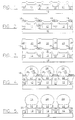
- microelectronic substrate 10 having a plurality of contact pads 12 thereon.
- microelectronic substrate 10 may be an integrated circuit chip, a circuit board or microelectronic package substrate, or any other substrate which requires electrical and mechanical connection.
- Contact pads 12 are formed on substrate 10 using well known techniques which need not be described herein.
- the contact pads are typically aluminium for integrated circuit chips, although other metals and metal composites may also be used for integrated circuit chips and other substrates.
- a passivating dielectric 14 is formed on the substrate 10 and patterned to expose the contact pads 12, using conventional plasma or reactive ion etching or other well known patterning techniques.
- a continuous under-bump metallurgy 16 is then formed on the substrate over the contact pads 12 and between the contact pads 12.
- the under-bump metallurgy 16 typically contains a (bottom) chromium layer (about 1000 ⁇ thick) adjacent substrate 10 and pads 12, which functions as an adhesion layer and diffusion barrier for the under-bump metallurgy.
- solder pads 20 are then formed on substrate 10, typically by electroplating. Volume is acquired by filling the spaces between the solder retaining walls 28 during plating. The solder pads 20 may be confined within the gaps in the solder dam layer 18 or may be allowed to extend over the solder dams, as is illustrated in Figure 3. The solder retaining walls 28 may then be removed.
- reflow preferably takes place for 1-2 minutes above the melting point of the solder.
- the unconverted copper in the phased chromium-copper region prevents detachment of the solder bumps from the chromium adhesion layer, and thereby enhances structural integrity.
- solder dams 18 prevent lateral spread and bridging of the solder and thereby control the size of the solder bump base.
- Reflow may be performed in air or in an inert ambient such as nitrogen, typically with flux applied, or in a reducing ambient such as hydrogen, without flux.
- flux residues if present, should be cleaned prior to etching the solder dam 18 and the under-bump metallurgy 16.
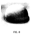
- each bump includes a lip or ridge 26 which typically extends several micrometers from the bump.
- This lip or ridge may be used to identify solder bumps formed according to the present invention, because lateral reaction with the under-bump metallurgy cannot take place if all under-bump metallurgy between the contact pads is removed prior to reflow.
- This lip or ridge 26 also provides an added degree of protection for the base of the solder bump. An improved performance solder bump is thereby provided.
- solder dam 18 and the under-bump metallurgy 16 between the contact pads 12 are removed, while preserving the base of the reflowed solder bumps 24. Since the top copper layer of the under-bump metallurgy between solder bump 24 and contact pad 12 has been converted into an intermetallic layer, the solder dams and the remaining under-bump metallurgy between contact pads 12 may be removed, without substantially removing the intermetallic.
- An etchant or etchants are used which etch the intermetallic 22 much more slowly than solder dam 18 and under-bump metallurgy 16. Preferably, the etchants do not etch the under-bump metallurgy 16 while removing solder dams 18 and intermetallic 22.
- a hydrochloric acid based etchant such as Transene CRE473 is an effective etchant, and a mixture of ammonium hydroxide and a trace amount of hydrogen peroxide is an effective copper etchant.
- Contact to the metal surface in the substrate with a zinc rod may be required to initiate etching of chromium.
- a mixture of ammonium hydroxide and hydrogen peroxide typically higher peroxide concentrations than in the copper etchant
- Multiple etch cycles may be needed to remove the phased chromium copper layer and the bottom chromium layer.
- etchants are effective against the copper/tin intermetallic and neither of these etchants attacks solder to a detectable extent. It will be understood by those having skill in the art that during copper etching, the device may be left in the etchant for as long as necessary to completely remove the copper between the bumps. It will also be understood by those having skill in the art that other etchants may be used, and other removal processes may be used.
- solder bump fabrication process is provided. Imperfections in photolithographic processing of thick film photoresists also do not degrade alignment. Moreover, undercutting of the solder bump base during under-bump metallurgy etching is substantially reduced or eliminated. The base geometry of the solder bump is therefore preserved. In fact, the process preferably forms a lip at the base of the solder bump to further protect the solder bump, and enhance electrical and mechanical reliability.
- Figure 6 is a scanning electron microscope photograph of a solder bump formed according to the present invention, illustrating solder bump 24, lip 26 and substrate 10.
- reduced bump base undercutting may be obtained with the present invention, independent of misalignment/distortion reduction, by reflowing the solder prior to removing the under-bump metallurgy between the contact pads.
- the designed bump base may be substantially larger than the contact pads, so that alignment of the solder bump to the contact pads is relatively unimportant. Misalignment -or distortion of the solder bump relative to the contact pads may be tolerated.
- the under-bump metallurgy may contain the same bottom chromium layer, phased chromium/copper layer and top copper layer described above. However, a second chromium layer is added on the top copper layer. Solder retaining walls made, for example, of thick film photoresist, are formed and patterned as described above. The patterned solder dam layer described above is not formed.
Landscapes
- Engineering & Computer Science (AREA)
- Manufacturing & Machinery (AREA)
- Computer Hardware Design (AREA)
- Microelectronics & Electronic Packaging (AREA)
- Power Engineering (AREA)
- Condensed Matter Physics & Semiconductors (AREA)
- Physics & Mathematics (AREA)
- General Physics & Mathematics (AREA)
- Electric Connection Of Electric Components To Printed Circuits (AREA)
- Wire Bonding (AREA)
- Ceramic Products (AREA)
- Arc Welding In General (AREA)
- Internal Circuitry In Semiconductor Integrated Circuit Devices (AREA)
Applications Claiming Priority (3)
| Application Number | Priority Date | Filing Date | Title |
|---|---|---|---|
| US07/759,450 US5162257A (en) | 1991-09-13 | 1991-09-13 | Solder bump fabrication method |
| US759450 | 1991-09-13 | ||
| PCT/US1992/007722 WO1993006620A1 (en) | 1991-09-13 | 1992-09-11 | Solder bump fabrication method and solder bumps formed thereby |
Publications (2)
| Publication Number | Publication Date |
|---|---|
| EP0603296A1 EP0603296A1 (en) | 1994-06-29 |
| EP0603296B1 true EP0603296B1 (en) | 1997-08-13 |
Family
ID=25055684
Family Applications (1)
| Application Number | Title | Priority Date | Filing Date |
|---|---|---|---|
| EP92919808A Expired - Lifetime EP0603296B1 (en) | 1991-09-13 | 1992-09-11 | Solder bump fabrication method and solder bumps formed thereby |
Country Status (10)
| Country | Link |
|---|---|
| US (2) | US5162257A (enExample) |
| EP (1) | EP0603296B1 (enExample) |
| JP (1) | JP2842692B2 (enExample) |
| KR (1) | KR0186061B1 (enExample) |
| AT (1) | ATE156935T1 (enExample) |
| CA (1) | CA2116766C (enExample) |
| DE (1) | DE69221627T2 (enExample) |
| ES (1) | ES2106194T3 (enExample) |
| TW (1) | TW200417B (enExample) |
| WO (1) | WO1993006620A1 (enExample) |
Cited By (11)
| Publication number | Priority date | Publication date | Assignee | Title |
|---|---|---|---|---|
| US5937320A (en) * | 1998-04-08 | 1999-08-10 | International Business Machines Corporation | Barrier layers for electroplated SnPb eutectic solder joints |
| US6960828B2 (en) | 2002-06-25 | 2005-11-01 | Unitive International Limited | Electronic structures including conductive shunt layers |
| US7081404B2 (en) | 2003-02-18 | 2006-07-25 | Unitive Electronics Inc. | Methods of selectively bumping integrated circuit substrates and related structures |
| US7156284B2 (en) | 2000-12-15 | 2007-01-02 | Unitive International Limited | Low temperature methods of bonding components and related structures |
| US7213740B2 (en) | 2000-11-10 | 2007-05-08 | Unitive International Limited | Optical structures including liquid bumps and related methods |
| US7358174B2 (en) | 2004-04-13 | 2008-04-15 | Amkor Technology, Inc. | Methods of forming solder bumps on exposed metal pads |
| US7531898B2 (en) | 2002-06-25 | 2009-05-12 | Unitive International Limited | Non-Circular via holes for bumping pads and related structures |
| US7547623B2 (en) | 2002-06-25 | 2009-06-16 | Unitive International Limited | Methods of forming lead free solder bumps |
| US7674701B2 (en) | 2006-02-08 | 2010-03-09 | Amkor Technology, Inc. | Methods of forming metal layers using multi-layer lift-off patterns |
| US7834454B2 (en) | 2004-03-10 | 2010-11-16 | Unitive International Limited | Electronic structures including barrier layers defining lips |
| US7932615B2 (en) | 2006-02-08 | 2011-04-26 | Amkor Technology, Inc. | Electronic devices including solder bumps on compliant dielectric layers |
Families Citing this family (85)
| Publication number | Priority date | Publication date | Assignee | Title |
|---|---|---|---|---|
| KR950001962A (ko) * | 1993-06-30 | 1995-01-04 | 김광호 | 반도체 칩 범프 |
| US5366140A (en) * | 1993-09-30 | 1994-11-22 | Minnesota Mining And Manufacturing Company | Patterned array of uniform metal microbeads |
| US5442852A (en) * | 1993-10-26 | 1995-08-22 | Pacific Microelectronics Corporation | Method of fabricating solder ball array |
| US5396702A (en) * | 1993-12-15 | 1995-03-14 | At&T Corp. | Method for forming solder bumps on a substrate using an electrodeposition technique |
| US5532550A (en) * | 1993-12-30 | 1996-07-02 | Adler; Robert | Organic based led display matrix |
| US5665639A (en) * | 1994-02-23 | 1997-09-09 | Cypress Semiconductor Corp. | Process for manufacturing a semiconductor device bump electrode using a rapid thermal anneal |
| US5470787A (en) * | 1994-05-02 | 1995-11-28 | Motorola, Inc. | Semiconductor device solder bump having intrinsic potential for forming an extended eutectic region and method for making and using the same |
| US5503286A (en) * | 1994-06-28 | 1996-04-02 | International Business Machines Corporation | Electroplated solder terminal |
| US5539153A (en) * | 1994-08-08 | 1996-07-23 | Hewlett-Packard Company | Method of bumping substrates by contained paste deposition |
| TW253856B (en) * | 1994-12-13 | 1995-08-11 | At & T Corp | Method of solder bonding, and article produced by the method |
| DE69617928T2 (de) | 1995-03-20 | 2002-07-18 | Unitive International Ltd., Curacao | Löthöcker-herstellungsverfahren und strukturen mit einer titan-sperrschicht |
| US6388203B1 (en) | 1995-04-04 | 2002-05-14 | Unitive International Limited | Controlled-shaped solder reservoirs for increasing the volume of solder bumps, and structures formed thereby |
| WO1996031905A1 (en) | 1995-04-05 | 1996-10-10 | Mcnc | A solder bump structure for a microelectronic substrate |
| US5620131A (en) * | 1995-06-15 | 1997-04-15 | Lucent Technologies Inc. | Method of solder bonding |
| US5874782A (en) * | 1995-08-24 | 1999-02-23 | International Business Machines Corporation | Wafer with elevated contact structures |
| KR100438256B1 (ko) * | 1995-12-18 | 2004-08-25 | 마츠시타 덴끼 산교 가부시키가이샤 | 반도체장치 및 그 제조방법 |
| US5736456A (en) * | 1996-03-07 | 1998-04-07 | Micron Technology, Inc. | Method of forming conductive bumps on die for flip chip applications |
| US5851911A (en) | 1996-03-07 | 1998-12-22 | Micron Technology, Inc. | Mask repattern process |
| US5793116A (en) * | 1996-05-29 | 1998-08-11 | Mcnc | Microelectronic packaging using arched solder columns |
| JP3413020B2 (ja) * | 1996-07-17 | 2003-06-03 | 株式会社東芝 | 半導体装置の製造方法 |
| US5903058A (en) * | 1996-07-17 | 1999-05-11 | Micron Technology, Inc. | Conductive bumps on die for flip chip application |
| US5902686A (en) * | 1996-11-21 | 1999-05-11 | Mcnc | Methods for forming an intermetallic region between a solder bump and an under bump metallurgy layer and related structures |
| JP3553300B2 (ja) * | 1996-12-02 | 2004-08-11 | 富士通株式会社 | 半導体装置の製造方法及び半導体装置の実装方法 |
| US6045030A (en) * | 1997-03-13 | 2000-04-04 | Raytheon Company | Sealing electronic packages containing bumped hybrids |
| US6117299A (en) * | 1997-05-09 | 2000-09-12 | Mcnc | Methods of electroplating solder bumps of uniform height on integrated circuit substrates |
| US5926731A (en) * | 1997-07-02 | 1999-07-20 | Delco Electronics Corp. | Method for controlling solder bump shape and stand-off height |
| US5990472A (en) * | 1997-09-29 | 1999-11-23 | Mcnc | Microelectronic radiation detectors for detecting and emitting radiation signals |
| US5962151A (en) * | 1997-12-05 | 1999-10-05 | Delco Electronics Corp. | Method for controlling solderability of a conductor and conductor formed thereby |
| US6595408B1 (en) * | 1998-10-07 | 2003-07-22 | Micron Technology, Inc. | Method of attaching solder balls to BGA package utilizing a tool to pick and dip the solder ball in flux prior to placement |
| US6268275B1 (en) | 1998-10-08 | 2001-07-31 | Micron Technology, Inc. | Method of locating conductive spheres utilizing screen and hopper of solder balls |
| US6139972A (en) * | 1998-10-26 | 2000-10-31 | Agilent Technologies Inc. | Solder paste containment device |
| JP3667184B2 (ja) * | 1999-02-26 | 2005-07-06 | 住友ベークライト株式会社 | 半導体装置 |
| JP3287328B2 (ja) * | 1999-03-09 | 2002-06-04 | 日本電気株式会社 | 半導体装置及び半導体装置の製造方法 |
| US6649533B1 (en) * | 1999-05-05 | 2003-11-18 | Advanced Micro Devices, Inc. | Method and apparatus for forming an under bump metallurgy layer |
| US6332988B1 (en) | 1999-06-02 | 2001-12-25 | International Business Machines Corporation | Rework process |
| US6544880B1 (en) * | 1999-06-14 | 2003-04-08 | Micron Technology, Inc. | Method of improving copper interconnects of semiconductor devices for bonding |
| US6570251B1 (en) | 1999-09-02 | 2003-05-27 | Micron Technology, Inc. | Under bump metalization pad and solder bump connections |
| KR100319813B1 (ko) | 2000-01-03 | 2002-01-09 | 윤종용 | 유비엠 언더컷을 개선한 솔더 범프의 형성 방법 |
| US6387793B1 (en) | 2000-03-09 | 2002-05-14 | Hrl Laboratories, Llc | Method for manufacturing precision electroplated solder bumps |
| US6437669B1 (en) * | 2000-09-29 | 2002-08-20 | Applied Micro Circuits Corporation | Microwave to millimeter wave frequency substrate interface |
| US6884313B2 (en) * | 2001-01-08 | 2005-04-26 | Fujitsu Limited | Method and system for joining and an ultra-high density interconnect |
| US6793792B2 (en) * | 2001-01-12 | 2004-09-21 | Unitive International Limited Curaco | Electroplating methods including maintaining a determined electroplating voltage and related systems |
| JP4656275B2 (ja) * | 2001-01-15 | 2011-03-23 | 日本電気株式会社 | 半導体装置の製造方法 |
| US6419148B1 (en) | 2001-01-23 | 2002-07-16 | Orbotech Ltd. | System for forming bumps on wafers |
| US6762122B2 (en) * | 2001-09-27 | 2004-07-13 | Unitivie International Limited | Methods of forming metallurgy structures for wire and solder bonding |
| TW536766B (en) * | 2002-02-19 | 2003-06-11 | Advanced Semiconductor Eng | Bump process |
| TW521359B (en) * | 2002-02-20 | 2003-02-21 | Advanced Semiconductor Eng | Bump fabrication process |
| TWI239578B (en) * | 2002-02-21 | 2005-09-11 | Advanced Semiconductor Eng | Manufacturing process of bump |
| US6987307B2 (en) * | 2002-06-26 | 2006-01-17 | Georgia Tech Research Corporation | Stand-alone organic-based passive devices |
| US7260890B2 (en) * | 2002-06-26 | 2007-08-28 | Georgia Tech Research Corporation | Methods for fabricating three-dimensional all organic interconnect structures |
| US6900708B2 (en) * | 2002-06-26 | 2005-05-31 | Georgia Tech Research Corporation | Integrated passive devices fabricated utilizing multi-layer, organic laminates |
| US6780751B2 (en) | 2002-10-09 | 2004-08-24 | Freescale Semiconductor, Inc. | Method for eliminating voiding in plated solder |
| US7495326B2 (en) | 2002-10-22 | 2009-02-24 | Unitive International Limited | Stacked electronic structures including offset substrates |
| US6897141B2 (en) * | 2002-10-23 | 2005-05-24 | Ocube Digital Co., Ltd. | Solder terminal and fabricating method thereof |
| US6796482B2 (en) * | 2002-10-31 | 2004-09-28 | Freescale Semiconductor, Inc. | Phase separated system for fluxing |
| DE10301934A1 (de) * | 2003-01-20 | 2004-07-29 | Epcos Ag | Elektrisches Bauelement mit verringerter Substratfläche |
| US7489914B2 (en) * | 2003-03-28 | 2009-02-10 | Georgia Tech Research Corporation | Multi-band RF transceiver with passive reuse in organic substrates |
| TWI221334B (en) * | 2003-06-30 | 2004-09-21 | Advanced Semiconductor Eng | Bumping process |
| TWI223882B (en) * | 2003-06-30 | 2004-11-11 | Advanced Semiconductor Eng | Bumping process |
| US7244671B2 (en) * | 2003-07-25 | 2007-07-17 | Unitive International Limited | Methods of forming conductive structures including titanium-tungsten base layers and related structures |
| US7049216B2 (en) | 2003-10-14 | 2006-05-23 | Unitive International Limited | Methods of providing solder structures for out plane connections |
| US7410833B2 (en) * | 2004-03-31 | 2008-08-12 | International Business Machines Corporation | Interconnections for flip-chip using lead-free solders and having reaction barrier layers |
| US8345433B2 (en) * | 2004-07-08 | 2013-01-01 | Avx Corporation | Heterogeneous organic laminate stack ups for high frequency applications |
| JP2006032851A (ja) * | 2004-07-21 | 2006-02-02 | Mitsui Mining & Smelting Co Ltd | 被覆銅、ホイスカの発生抑制方法、プリント配線基板および半導体装置 |
| US7252514B2 (en) * | 2004-09-02 | 2007-08-07 | International Business Machines Corporation | High density space transformer and method of fabricating same |
| US20060205170A1 (en) * | 2005-03-09 | 2006-09-14 | Rinne Glenn A | Methods of forming self-healing metal-insulator-metal (MIM) structures and related devices |
| US7439840B2 (en) | 2006-06-27 | 2008-10-21 | Jacket Micro Devices, Inc. | Methods and apparatuses for high-performing multi-layer inductors |
| US7808434B2 (en) * | 2006-08-09 | 2010-10-05 | Avx Corporation | Systems and methods for integrated antennae structures in multilayer organic-based printed circuit devices |
| JP2010501116A (ja) * | 2006-08-17 | 2010-01-14 | エヌエックスピー ビー ヴィ | エッチングステップ中の電極の適正なアンダーカットの試験方法 |
| US7989895B2 (en) * | 2006-11-15 | 2011-08-02 | Avx Corporation | Integration using package stacking with multi-layer organic substrates |
| US7569164B2 (en) * | 2007-01-29 | 2009-08-04 | Harima Chemicals, Inc. | Solder precoating method |
| CN101234455B (zh) * | 2007-01-30 | 2012-03-28 | 播磨化成株式会社 | 焊锡膏组合物及焊锡预涂法 |
| EP1952935B1 (en) * | 2007-02-01 | 2016-05-11 | Harima Chemicals, Inc. | Solder paste composition and solder precoating method |
| US7713860B2 (en) * | 2007-10-13 | 2010-05-11 | Wan-Ling Yu | Method of forming metallic bump on I/O pad |
| TWI446843B (zh) * | 2007-12-11 | 2014-07-21 | Unimicron Technology Corp | 線路板及其製程 |
| US7888259B2 (en) * | 2008-08-19 | 2011-02-15 | Ati Technologies Ulc | Integrated circuit package employing predetermined three-dimensional solder pad surface and method for making same |
| KR101022942B1 (ko) | 2008-11-12 | 2011-03-16 | 삼성전기주식회사 | 흐름 방지용 댐을 구비한 인쇄회로기판 및 그 제조방법 |
| US9142520B2 (en) * | 2011-08-30 | 2015-09-22 | Ati Technologies Ulc | Methods of fabricating semiconductor chip solder structures |
| KR101774938B1 (ko) | 2011-08-31 | 2017-09-06 | 삼성전자 주식회사 | 지지대를 갖는 반도체 패키지 및 그 형성 방법 |
| US8946891B1 (en) * | 2012-09-04 | 2015-02-03 | Amkor Technology, Inc. | Mushroom shaped bump on repassivation |
| US20150195912A1 (en) | 2014-01-08 | 2015-07-09 | Zhuhai Advanced Chip Carriers & Electronic Substrate Solutions Technologies Co. Ltd. | Substrates With Ultra Fine Pitch Flip Chip Bumps |
| US9949378B2 (en) | 2014-04-14 | 2018-04-17 | Presidio Components, Inc. | Electrical devices with solder dam |
| FR3050865B1 (fr) * | 2016-05-02 | 2018-10-12 | Commissariat A L'energie Atomique Et Aux Energies Alternatives | Procede de realisation d'interconnexions conductrices sur un substrat et interconnexions ainsi obtenues |
| US11676932B2 (en) * | 2019-12-31 | 2023-06-13 | Micron Technology, Inc. | Semiconductor interconnect structures with narrowed portions, and associated systems and methods |
| KR20250061993A (ko) | 2023-10-30 | 2025-05-08 | 가톨릭대학교 산학협력단 | 재난 대응 하·폐수 처리시설의 자산관리방법 |
Family Cites Families (19)
| Publication number | Priority date | Publication date | Assignee | Title |
|---|---|---|---|---|
| US3986255A (en) * | 1974-11-29 | 1976-10-19 | Itek Corporation | Process for electrically interconnecting chips with substrates employing gold alloy bumps and magnetic materials therein |
| JPS54128669A (en) * | 1978-03-29 | 1979-10-05 | Nippon Denso Co Ltd | Flip chip element |
| US4273859A (en) * | 1979-12-31 | 1981-06-16 | Honeywell Information Systems Inc. | Method of forming solder bump terminals on semiconductor elements |
| EP0229850B1 (en) * | 1985-07-16 | 1992-06-10 | Nippon Telegraph and Telephone Corporation | Connection terminals between substrates and method of producing the same |
| FR2588121B1 (fr) * | 1985-10-02 | 1990-02-23 | Bull Sa | Procede et dispositif de soudage d'elements sur les plots correspondants d'une plaquette telle que notamment une plaquette de circuits integres de haute densite |
| US4878611A (en) * | 1986-05-30 | 1989-11-07 | American Telephone And Telegraph Company, At&T Bell Laboratories | Process for controlling solder joint geometry when surface mounting a leadless integrated circuit package on a substrate |
| US4763829A (en) * | 1986-06-04 | 1988-08-16 | American Telephone And Telegraph Company, At&T Bell Laboratories | Soldering of electronic components |
| DE3684602D1 (de) * | 1986-10-08 | 1992-04-30 | Ibm | Verfahren zum herstellen von loetkontakten fuer ein keramisches modul ohne steckerstifte. |
| US4752027A (en) * | 1987-02-20 | 1988-06-21 | Hewlett-Packard Company | Method and apparatus for solder bumping of printed circuit boards |
| JP2544396B2 (ja) * | 1987-08-25 | 1996-10-16 | 株式会社日立製作所 | 半導体集積回路装置の製造方法 |
| JP2633586B2 (ja) * | 1987-10-21 | 1997-07-23 | 株式会社東芝 | バンプ構造を有する半導体装置 |
| US4817850A (en) * | 1988-03-28 | 1989-04-04 | Hughes Aircraft Company | Repairable flip-chip bumping |
| US4840302A (en) * | 1988-04-15 | 1989-06-20 | International Business Machines Corporation | Chromium-titanium alloy |
| US4893403A (en) * | 1988-04-15 | 1990-01-16 | Hewlett-Packard Company | Chip alignment method |
| US4950623A (en) * | 1988-08-02 | 1990-08-21 | Microelectronics Center Of North Carolina | Method of building solder bumps |
| US5024372A (en) * | 1989-01-03 | 1991-06-18 | Motorola, Inc. | Method of making high density solder bumps and a substrate socket for high density solder bumps |
| US4940181A (en) * | 1989-04-06 | 1990-07-10 | Motorola, Inc. | Pad grid array for receiving a solder bumped chip carrier |
| US5154341A (en) * | 1990-12-06 | 1992-10-13 | Motorola Inc. | Noncollapsing multisolder interconnection |
| US5152451A (en) * | 1991-04-01 | 1992-10-06 | Motorola, Inc. | Controlled solder oxidation process |
-
1991
- 1991-09-13 US US07/759,450 patent/US5162257A/en not_active Expired - Lifetime
-
1992
- 1992-08-07 US US07/927,069 patent/US5293006A/en not_active Expired - Lifetime
- 1992-09-11 WO PCT/US1992/007722 patent/WO1993006620A1/en not_active Ceased
- 1992-09-11 DE DE69221627T patent/DE69221627T2/de not_active Expired - Fee Related
- 1992-09-11 AT AT92919808T patent/ATE156935T1/de not_active IP Right Cessation
- 1992-09-11 KR KR1019940700820A patent/KR0186061B1/ko not_active Expired - Fee Related
- 1992-09-11 ES ES92919808T patent/ES2106194T3/es not_active Expired - Lifetime
- 1992-09-11 EP EP92919808A patent/EP0603296B1/en not_active Expired - Lifetime
- 1992-09-11 JP JP5506136A patent/JP2842692B2/ja not_active Expired - Fee Related
- 1992-09-11 CA CA002116766A patent/CA2116766C/en not_active Expired - Fee Related
- 1992-10-01 TW TW081107808A patent/TW200417B/zh active
Cited By (17)
| Publication number | Priority date | Publication date | Assignee | Title |
|---|---|---|---|---|
| US5937320A (en) * | 1998-04-08 | 1999-08-10 | International Business Machines Corporation | Barrier layers for electroplated SnPb eutectic solder joints |
| US7213740B2 (en) | 2000-11-10 | 2007-05-08 | Unitive International Limited | Optical structures including liquid bumps and related methods |
| US7156284B2 (en) | 2000-12-15 | 2007-01-02 | Unitive International Limited | Low temperature methods of bonding components and related structures |
| US7547623B2 (en) | 2002-06-25 | 2009-06-16 | Unitive International Limited | Methods of forming lead free solder bumps |
| US7879715B2 (en) | 2002-06-25 | 2011-02-01 | Unitive International Limited | Methods of forming electronic structures including conductive shunt layers and related structures |
| US7297631B2 (en) | 2002-06-25 | 2007-11-20 | Unitive International Limited | Methods of forming electronic structures including conductive shunt layers and related structures |
| US8294269B2 (en) | 2002-06-25 | 2012-10-23 | Unitive International | Electronic structures including conductive layers comprising copper and having a thickness of at least 0.5 micrometers |
| US7531898B2 (en) | 2002-06-25 | 2009-05-12 | Unitive International Limited | Non-Circular via holes for bumping pads and related structures |
| US6960828B2 (en) | 2002-06-25 | 2005-11-01 | Unitive International Limited | Electronic structures including conductive shunt layers |
| US7839000B2 (en) | 2002-06-25 | 2010-11-23 | Unitive International Limited | Solder structures including barrier layers with nickel and/or copper |
| US7579694B2 (en) | 2003-02-18 | 2009-08-25 | Unitive International Limited | Electronic devices including offset conductive bumps |
| US7081404B2 (en) | 2003-02-18 | 2006-07-25 | Unitive Electronics Inc. | Methods of selectively bumping integrated circuit substrates and related structures |
| US7834454B2 (en) | 2004-03-10 | 2010-11-16 | Unitive International Limited | Electronic structures including barrier layers defining lips |
| US8487432B2 (en) | 2004-03-10 | 2013-07-16 | Amkor Technology, Inc. | Electronic structures including barrier layers and/or oxidation barriers defining lips and related methods |
| US7358174B2 (en) | 2004-04-13 | 2008-04-15 | Amkor Technology, Inc. | Methods of forming solder bumps on exposed metal pads |
| US7674701B2 (en) | 2006-02-08 | 2010-03-09 | Amkor Technology, Inc. | Methods of forming metal layers using multi-layer lift-off patterns |
| US7932615B2 (en) | 2006-02-08 | 2011-04-26 | Amkor Technology, Inc. | Electronic devices including solder bumps on compliant dielectric layers |
Also Published As
| Publication number | Publication date |
|---|---|
| ES2106194T3 (es) | 1997-11-01 |
| DE69221627D1 (de) | 1997-09-18 |
| CA2116766A1 (en) | 1993-04-01 |
| KR0186061B1 (ko) | 1999-04-15 |
| DE69221627T2 (de) | 1998-01-08 |
| EP0603296A1 (en) | 1994-06-29 |
| TW200417B (enExample) | 1993-02-21 |
| US5162257A (en) | 1992-11-10 |
| WO1993006620A1 (en) | 1993-04-01 |
| KR940702644A (ko) | 1994-08-20 |
| US5293006A (en) | 1994-03-08 |
| ATE156935T1 (de) | 1997-08-15 |
| JP2842692B2 (ja) | 1999-01-06 |
| JPH07502147A (ja) | 1995-03-02 |
| CA2116766C (en) | 1999-02-16 |
Similar Documents
| Publication | Publication Date | Title |
|---|---|---|
| EP0603296B1 (en) | Solder bump fabrication method and solder bumps formed thereby | |
| EP1134805B1 (en) | Solder bump fabrication methods and structure including a titanium barrier layer | |
| EP1032030B1 (en) | Flip chip bump bonding | |
| US6111321A (en) | Ball limiting metalization process for interconnection | |
| US6936923B2 (en) | Method to form very a fine pitch solder bump using methods of electroplating | |
| US5492235A (en) | Process for single mask C4 solder bump fabrication | |
| US7816787B2 (en) | Method of forming low stress multi-layer metallurgical structures and high reliable lead free solder termination electrodes | |
| KR100510543B1 (ko) | 표면 결함이 제거된 범프 형성 방법 | |
| US5620611A (en) | Method to improve uniformity and reduce excess undercuts during chemical etching in the manufacture of solder pads | |
| US6943101B2 (en) | Manufacturing of a corrosion protected interconnect on a substrate | |
| EP0657923A2 (en) | Method of protecting a solder ball during an etch process, by applying a resist around the base of the solder ball | |
| US6911390B2 (en) | Fabrication method for an interconnect on a substrate | |
| US20020086512A1 (en) | Method of forming solder bumps | |
| US20040124171A1 (en) | [bump-forming process] | |
| CN1103119C (zh) | 用于单掩膜c4焊料凸点制造的方法 | |
| US20080119056A1 (en) | Method for improved copper layer etching of wafers with c4 connection structures | |
| KR950005270B1 (ko) | 표면실장형 반도체 패키지의 범퍼형성방법 | |
| KR100212496B1 (ko) | 플립칩용 반도체 장치의 제조방법 | |
| HK1036523B (en) | Solder bump fabrication methods and structure including a titanium barrier layer | |
| KR20020071096A (ko) | 솔더 범프의 형성 방법 |
Legal Events
| Date | Code | Title | Description |
|---|---|---|---|
| PUAI | Public reference made under article 153(3) epc to a published international application that has entered the european phase |
Free format text: ORIGINAL CODE: 0009012 |
|
| 17P | Request for examination filed |
Effective date: 19940304 |
|
| AK | Designated contracting states |
Kind code of ref document: A1 Designated state(s): AT BE CH DE DK ES FR GB GR IE IT LI LU MC NL SE |
|
| GRAG | Despatch of communication of intention to grant |
Free format text: ORIGINAL CODE: EPIDOS AGRA |
|
| 17Q | First examination report despatched |
Effective date: 19960709 |
|
| GRAH | Despatch of communication of intention to grant a patent |
Free format text: ORIGINAL CODE: EPIDOS IGRA |
|
| GRAH | Despatch of communication of intention to grant a patent |
Free format text: ORIGINAL CODE: EPIDOS IGRA |
|
| GRAA | (expected) grant |
Free format text: ORIGINAL CODE: 0009210 |
|
| AK | Designated contracting states |
Kind code of ref document: B1 Designated state(s): AT BE CH DE DK ES FR GB GR IE IT LI LU MC NL SE |
|
| PG25 | Lapsed in a contracting state [announced via postgrant information from national office to epo] |
Ref country code: LI Free format text: LAPSE BECAUSE OF FAILURE TO SUBMIT A TRANSLATION OF THE DESCRIPTION OR TO PAY THE FEE WITHIN THE PRESCRIBED TIME-LIMIT Effective date: 19970813 Ref country code: GR Free format text: LAPSE BECAUSE OF FAILURE TO SUBMIT A TRANSLATION OF THE DESCRIPTION OR TO PAY THE FEE WITHIN THE PRESCRIBED TIME-LIMIT Effective date: 19970813 Ref country code: DK Free format text: LAPSE BECAUSE OF NON-PAYMENT OF DUE FEES Effective date: 19970813 Ref country code: CH Free format text: LAPSE BECAUSE OF FAILURE TO SUBMIT A TRANSLATION OF THE DESCRIPTION OR TO PAY THE FEE WITHIN THE PRESCRIBED TIME-LIMIT Effective date: 19970813 Ref country code: AT Effective date: 19970813 |
|
| REF | Corresponds to: |
Ref document number: 156935 Country of ref document: AT Date of ref document: 19970815 Kind code of ref document: T |
|
| REG | Reference to a national code |
Ref country code: CH Ref legal event code: EP |
|
| REF | Corresponds to: |
Ref document number: 69221627 Country of ref document: DE Date of ref document: 19970918 |
|
| PG25 | Lapsed in a contracting state [announced via postgrant information from national office to epo] |
Ref country code: LU Free format text: LAPSE BECAUSE OF NON-PAYMENT OF DUE FEES Effective date: 19970930 |
|
| ET | Fr: translation filed | ||
| REG | Reference to a national code |
Ref country code: ES Ref legal event code: FG2A Ref document number: 2106194 Country of ref document: ES Kind code of ref document: T3 |
|
| ITF | It: translation for a ep patent filed | ||
| PG25 | Lapsed in a contracting state [announced via postgrant information from national office to epo] |
Ref country code: SE Effective date: 19971113 |
|
| REG | Reference to a national code |
Ref country code: CH Ref legal event code: PL |
|
| PG25 | Lapsed in a contracting state [announced via postgrant information from national office to epo] |
Ref country code: MC Free format text: LAPSE BECAUSE OF NON-PAYMENT OF DUE FEES Effective date: 19980331 |
|
| PLBE | No opposition filed within time limit |
Free format text: ORIGINAL CODE: 0009261 |
|
| STAA | Information on the status of an ep patent application or granted ep patent |
Free format text: STATUS: NO OPPOSITION FILED WITHIN TIME LIMIT |
|
| 26N | No opposition filed | ||
| REG | Reference to a national code |
Ref country code: GB Ref legal event code: IF02 |
|
| PGFP | Annual fee paid to national office [announced via postgrant information from national office to epo] |
Ref country code: NL Payment date: 20020930 Year of fee payment: 11 Ref country code: IE Payment date: 20020930 Year of fee payment: 11 |
|
| PGFP | Annual fee paid to national office [announced via postgrant information from national office to epo] |
Ref country code: ES Payment date: 20021030 Year of fee payment: 11 |
|
| PGFP | Annual fee paid to national office [announced via postgrant information from national office to epo] |
Ref country code: BE Payment date: 20021129 Year of fee payment: 11 |
|
| PG25 | Lapsed in a contracting state [announced via postgrant information from national office to epo] |
Ref country code: IE Free format text: LAPSE BECAUSE OF NON-PAYMENT OF DUE FEES Effective date: 20030911 |
|
| PG25 | Lapsed in a contracting state [announced via postgrant information from national office to epo] |
Ref country code: ES Free format text: LAPSE BECAUSE OF NON-PAYMENT OF DUE FEES Effective date: 20030912 |
|
| PG25 | Lapsed in a contracting state [announced via postgrant information from national office to epo] |
Ref country code: BE Free format text: LAPSE BECAUSE OF NON-PAYMENT OF DUE FEES Effective date: 20030930 |
|
| BERE | Be: lapsed |
Owner name: *MCNC Effective date: 20030930 |
|
| PG25 | Lapsed in a contracting state [announced via postgrant information from national office to epo] |
Ref country code: NL Free format text: LAPSE BECAUSE OF NON-PAYMENT OF DUE FEES Effective date: 20040401 |
|
| NLV4 | Nl: lapsed or anulled due to non-payment of the annual fee |
Effective date: 20040401 |
|
| REG | Reference to a national code |
Ref country code: IE Ref legal event code: MM4A |
|
| REG | Reference to a national code |
Ref country code: ES Ref legal event code: FD2A Effective date: 20030912 |
|
| PG25 | Lapsed in a contracting state [announced via postgrant information from national office to epo] |
Ref country code: IT Free format text: LAPSE BECAUSE OF NON-PAYMENT OF DUE FEES Effective date: 20050911 |
|
| PGFP | Annual fee paid to national office [announced via postgrant information from national office to epo] |
Ref country code: FR Payment date: 20060918 Year of fee payment: 15 |
|
| PGFP | Annual fee paid to national office [announced via postgrant information from national office to epo] |
Ref country code: GB Payment date: 20060925 Year of fee payment: 15 |
|
| PGFP | Annual fee paid to national office [announced via postgrant information from national office to epo] |
Ref country code: DE Payment date: 20061031 Year of fee payment: 15 |
|
| GBPC | Gb: european patent ceased through non-payment of renewal fee |
Effective date: 20070911 |
|
| PG25 | Lapsed in a contracting state [announced via postgrant information from national office to epo] |
Ref country code: DE Free format text: LAPSE BECAUSE OF NON-PAYMENT OF DUE FEES Effective date: 20080401 |
|
| REG | Reference to a national code |
Ref country code: FR Ref legal event code: ST Effective date: 20080531 |
|
| PG25 | Lapsed in a contracting state [announced via postgrant information from national office to epo] |
Ref country code: FR Free format text: LAPSE BECAUSE OF NON-PAYMENT OF DUE FEES Effective date: 20071001 |
|
| PG25 | Lapsed in a contracting state [announced via postgrant information from national office to epo] |
Ref country code: GB Free format text: LAPSE BECAUSE OF NON-PAYMENT OF DUE FEES Effective date: 20070911 |