EP0600853A2 - Gerät zum optischen Schreiben von Information - Google Patents
Gerät zum optischen Schreiben von Information Download PDFInfo
- Publication number
- EP0600853A2 EP0600853A2 EP94200320A EP94200320A EP0600853A2 EP 0600853 A2 EP0600853 A2 EP 0600853A2 EP 94200320 A EP94200320 A EP 94200320A EP 94200320 A EP94200320 A EP 94200320A EP 0600853 A2 EP0600853 A2 EP 0600853A2
- Authority
- EP
- European Patent Office
- Prior art keywords
- gate voltage
- array
- lens
- setting circuit
- resistors
- Prior art date
- Legal status (The legal status is an assumption and is not a legal conclusion. Google has not performed a legal analysis and makes no representation as to the accuracy of the status listed.)
- Ceased
Links
Images


Classifications
-
- G—PHYSICS
- G02—OPTICS
- G02B—OPTICAL ELEMENTS, SYSTEMS OR APPARATUS
- G02B3/00—Simple or compound lenses
- G02B3/0006—Arrays
- G02B3/0037—Arrays characterized by the distribution or form of lenses
- G02B3/005—Arrays characterized by the distribution or form of lenses arranged along a single direction only, e.g. lenticular sheets
-
- B—PERFORMING OPERATIONS; TRANSPORTING
- B41—PRINTING; LINING MACHINES; TYPEWRITERS; STAMPS
- B41J—TYPEWRITERS; SELECTIVE PRINTING MECHANISMS, i.e. MECHANISMS PRINTING OTHERWISE THAN FROM A FORME; CORRECTION OF TYPOGRAPHICAL ERRORS
- B41J2/00—Typewriters or selective printing mechanisms characterised by the printing or marking process for which they are designed
- B41J2/435—Typewriters or selective printing mechanisms characterised by the printing or marking process for which they are designed characterised by selective application of radiation to a printing material or impression-transfer material
- B41J2/447—Typewriters or selective printing mechanisms characterised by the printing or marking process for which they are designed characterised by selective application of radiation to a printing material or impression-transfer material using arrays of radiation sources
- B41J2/45—Typewriters or selective printing mechanisms characterised by the printing or marking process for which they are designed characterised by selective application of radiation to a printing material or impression-transfer material using arrays of radiation sources using light-emitting diode [LED] or laser arrays
- B41J2/451—Special optical means therefor, e.g. lenses, mirrors, focusing means
-
- G—PHYSICS
- G06—COMPUTING OR CALCULATING; COUNTING
- G06K—GRAPHICAL DATA READING; PRESENTATION OF DATA; RECORD CARRIERS; HANDLING RECORD CARRIERS
- G06K15/00—Arrangements for producing a permanent visual presentation of the output data, e.g. computer output printers
- G06K15/02—Arrangements for producing a permanent visual presentation of the output data, e.g. computer output printers using printers
- G06K15/12—Arrangements for producing a permanent visual presentation of the output data, e.g. computer output printers using printers by photographic printing, e.g. by laser printers
- G06K15/1238—Arrangements for producing a permanent visual presentation of the output data, e.g. computer output printers using printers by photographic printing, e.g. by laser printers simultaneously exposing more than one point
- G06K15/1242—Arrangements for producing a permanent visual presentation of the output data, e.g. computer output printers using printers by photographic printing, e.g. by laser printers simultaneously exposing more than one point on one main scanning line
- G06K15/1247—Arrangements for producing a permanent visual presentation of the output data, e.g. computer output printers using printers by photographic printing, e.g. by laser printers simultaneously exposing more than one point on one main scanning line using an array of light sources, e.g. a linear array
-
- H—ELECTRICITY
- H04—ELECTRIC COMMUNICATION TECHNIQUE
- H04N—PICTORIAL COMMUNICATION, e.g. TELEVISION
- H04N1/00—Scanning, transmission or reproduction of documents or the like, e.g. facsimile transmission; Details thereof
- H04N1/024—Details of scanning heads ; Means for illuminating the original
- H04N1/028—Details of scanning heads ; Means for illuminating the original for picture information pick-up
- H04N1/03—Details of scanning heads ; Means for illuminating the original for picture information pick-up with photodetectors arranged in a substantially linear array
- H04N1/0301—Details of scanning heads ; Means for illuminating the original for picture information pick-up with photodetectors arranged in a substantially linear array using a bent optical path between the scanned line and the photodetector array, e.g. a folded optical path
- H04N1/0303—Details of scanning heads ; Means for illuminating the original for picture information pick-up with photodetectors arranged in a substantially linear array using a bent optical path between the scanned line and the photodetector array, e.g. a folded optical path with the scanned line and the photodetector array lying in non-parallel planes
-
- H—ELECTRICITY
- H04—ELECTRIC COMMUNICATION TECHNIQUE
- H04N—PICTORIAL COMMUNICATION, e.g. TELEVISION
- H04N1/00—Scanning, transmission or reproduction of documents or the like, e.g. facsimile transmission; Details thereof
- H04N1/024—Details of scanning heads ; Means for illuminating the original
- H04N1/028—Details of scanning heads ; Means for illuminating the original for picture information pick-up
- H04N1/03—Details of scanning heads ; Means for illuminating the original for picture information pick-up with photodetectors arranged in a substantially linear array
- H04N1/0306—Details of scanning heads ; Means for illuminating the original for picture information pick-up with photodetectors arranged in a substantially linear array using a plurality of optical elements arrayed in the main scan direction, e.g. an array of lenses
-
- H—ELECTRICITY
- H04—ELECTRIC COMMUNICATION TECHNIQUE
- H04N—PICTORIAL COMMUNICATION, e.g. TELEVISION
- H04N1/00—Scanning, transmission or reproduction of documents or the like, e.g. facsimile transmission; Details thereof
- H04N1/024—Details of scanning heads ; Means for illuminating the original
- H04N1/032—Details of scanning heads ; Means for illuminating the original for picture information reproduction
- H04N1/036—Details of scanning heads ; Means for illuminating the original for picture information reproduction for optical reproduction
-
- H—ELECTRICITY
- H04—ELECTRIC COMMUNICATION TECHNIQUE
- H04N—PICTORIAL COMMUNICATION, e.g. TELEVISION
- H04N1/00—Scanning, transmission or reproduction of documents or the like, e.g. facsimile transmission; Details thereof
- H04N1/04—Scanning arrangements, i.e. arrangements for the displacement of active reading or reproducing elements relative to the original or reproducing medium, or vice versa
- H04N1/19—Scanning arrangements, i.e. arrangements for the displacement of active reading or reproducing elements relative to the original or reproducing medium, or vice versa using multi-element arrays
- H04N1/191—Scanning arrangements, i.e. arrangements for the displacement of active reading or reproducing elements relative to the original or reproducing medium, or vice versa using multi-element arrays the array comprising a one-dimensional [1D] array
- H04N1/192—Simultaneously or substantially simultaneously scanning picture elements on one main scanning line
- H04N1/193—Simultaneously or substantially simultaneously scanning picture elements on one main scanning line using electrically scanned linear arrays, e.g. linear CCD arrays
- H04N1/1934—Combination of arrays
-
- H—ELECTRICITY
- H04—ELECTRIC COMMUNICATION TECHNIQUE
- H04N—PICTORIAL COMMUNICATION, e.g. TELEVISION
- H04N1/00—Scanning, transmission or reproduction of documents or the like, e.g. facsimile transmission; Details thereof
- H04N1/04—Scanning arrangements, i.e. arrangements for the displacement of active reading or reproducing elements relative to the original or reproducing medium, or vice versa
- H04N1/19—Scanning arrangements, i.e. arrangements for the displacement of active reading or reproducing elements relative to the original or reproducing medium, or vice versa using multi-element arrays
- H04N1/191—Scanning arrangements, i.e. arrangements for the displacement of active reading or reproducing elements relative to the original or reproducing medium, or vice versa using multi-element arrays the array comprising a one-dimensional [1D] array
- H04N1/192—Simultaneously or substantially simultaneously scanning picture elements on one main scanning line
- H04N1/193—Simultaneously or substantially simultaneously scanning picture elements on one main scanning line using electrically scanned linear arrays, e.g. linear CCD arrays
- H04N1/1935—Optical means for mapping the whole or part of a scanned line onto the array
-
- H—ELECTRICITY
- H10—SEMICONDUCTOR DEVICES; ELECTRIC SOLID-STATE DEVICES NOT OTHERWISE PROVIDED FOR
- H10W—GENERIC PACKAGES, INTERCONNECTIONS, CONNECTORS OR OTHER CONSTRUCTIONAL DETAILS OF DEVICES COVERED BY CLASS H10
- H10W72/00—Interconnections or connectors in packages
- H10W72/851—Dispositions of multiple connectors or interconnections
- H10W72/874—On different surfaces
- H10W72/884—Die-attach connectors and bond wires
Definitions
- This invention relates to an apparatus, such as an optical printer or reader, for optically writing or reading information defined in the preamble of claim 1.
- optical printers include a row of light emitting diodes (LED) arranged to face a photosensitive drum in parallel thereto, and a lens system arranged between the diode row and the drum.
- the row of diodes are driven for lighting by respective control ICs to form a row of luminescent dots in various patterns depending on the driving control, each of the control ICs including drive transistors for activating the respective LEDs of the relevant control IC.
- the lens system serves to form an image of the luminescent dot row on the drum in rotation, thus effecting intended printing in accordance with the driving control.
- the drive current passing through the LEDs of each array chip varies depending on the characteristic of the corresponding control circuit IC and the gate voltage for the relevant drive transistors.
- the gate voltage separately with respect to all of the control circuits IC.
- a conventional way for such voltage adjustment is to provide a voltage dividing circuit arranged outside each control circuit IC for applying an adjusted gate voltage. More specifically, the voltage dividing circuit enables voltage adjustment through changing the voltage division ratio by selecting external resistors to be taken into the circuit.
- this manner of voltage adjustment it is difficult to minutely adjust the gate voltage because there is a limitation on the kinds of available resistors. Further, this manner of voltage adjustment is time-taking.
- an object of the present invention to provide an apparatus for optically writing or reading information which is capable of solving the above-described problem of the prior art.
- an apparatus for optically writing or reading information comprising a row of optical dot array chips, each array chip including a plurality of optical dot elements constantly arranged in the direction of said row, characterised in that: the respective array chips are driven by separate control circuits each incorporating a plurality of drive transistors for driving the respective optical dot elements of a corresponding array chip, each control circuit further incorporating a gate voltage setting circuit which applies an adjustable gate voltage to the respective drive transistors, said gate voltage setting circuit comprising a plurality of voltage dividing resistors only selected one or ones of which are incorporated into said gate voltage setting circuit while the other one or ones of the voltage dividing resistors remain non-connected.
- the plurality of voltage dividing resistors are incorporated in advance into the gate voltage setting circuit as internal components, and the gate voltage adjustment is performed by selecting only necessary one or ones of the voltage dividing resistors while making the unnecessary resistor or resistors remain non-connected.
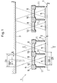
- an optical printer 1 which comprises an LED print head 2 arranged in facing relation to a photosensitive drum 3 in parallel thereto.
- a lens system 4 is disposed between the print head and the drum.
- the LED print head 2 includes a plurality (e.g. 16) of LED array chips 5 fixed in a longitudinal row on a substrate 6 as constantly spaced from each other.
- Each chip 5 comprises a plurality (e.g. 64 or 128) of light emitting diodes disposed at constant minute spacing in a longitudinal array on a strip-form GaAsP wafer of a rectangular cross-section. When lit, each diode forms a luminescent dot.
- the print head further includes a heat sink 7 for preventing excessive heating of the LED array chip and the substrate.
- a single wafer having a large length is cut into chip lengths by dicing to provide a number of LED arrays chips at one time.
- the spacing between the array chips 5, which is constant, is determined in dependence on the magnification provided by the lens system 4. On the other hand, the spacing between the luminescent dots in each chip 5 is fixed irrespective of the magnification of the lens system.
- the distance between the print head 2 and the drum 3 is also determined by the characteristic and arrangement of the lens system 4.
- the lens system 4 includes a plurality of convex lenses 8 arranged in exact correspondence with the respective array chips 5.
- the pitch between the lenses is exactly the same as that between the array chips.
- Each lens may be aspherical and made of a hard resinous material to have little or negligible aberration.
- the lenses 8 are retained in place by an elongate lens holder 9 formed with lens holding bores 10 in exact correspondence with the array chips 5.
- the lens holder may be supported at both longitudinal ends (not shown in Figures 1 and 2) on the heat sink 7 in a manner such that the holder is minutely adjustable in level.
- the holder may be made either of a synthetic resin or a metal.
- the lens holder 9 is formed with light shielding partition walls 11 each extending toward a point between two adjacent array chips 5. Further, the holder has a pair of light shielding longitudinal walls 12. Thus, each array chip is substantially enclosed in a box space, so that the light from that particular chip will not leak into adjacent box spaces. Such light shielding serves to prevent deterioration in printing quality.
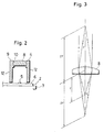
- the lens system 4 is arranged so that the distance between each lens 8 and the corresponding array chip 5 (object point) is larger than the focal length (f) of the lens but smaller than 2f (see Figure 3).
- the lens serves to form magnified images, in inverted arrangement, of the luminescent dots at the image point.
- the photosensitive drum 13 is located so that its image receiving surface is located at the image point.
- the pitch between two adjacent chips 5 is represented as D1
- D2 the distance between the two end dots (farthest dots) in each chip
- D2' the distance between the two end dot images of the same chip
- Y the spacing between two adjacent dot images of the same chip
- the magnification of the lenses 8, which is defined as D2'/D2 is advantegeously set to satisfy the following equation.
- D2'/D2 (D1-Y)/D2
- D2' D1-Y
- the lens holder 9 may be minutely adjusted in level within a range of allowable image blurring, thereby making the dot image spacing X exactly equal to Y.
- the respective array chips 5 there is no need to arrange the respective array chips 5 in end-to-end contact with each other. Therefore, strict dicing accuracy is no longer called for when manufacturing a number of array chips from a long wafer. As a result, the dicing step is much more simplified while drastically increasing the yield of production. Further, the reasonable spacing between the chips 5 reduces the likelihood of damaging or contaminating contact between them during chip bonding, thereby facilitating the bonding operation and ensuring a higher quality of the print head 2.
- the convex lenses 8 can be manufactured at a lower cost than the self-focusing microlenses which are currently in wide use. There has been established a technique for accurately manufacturing aspheric plastic lenses with little aberration. Thus, it is possible to enhance the quality of the optical system 4 to a sufficient extent for providing good printing quality.
- the lens holder 9 having level adjustability facilitates accurate mounting or positioning of the lenses 8. Further, the light shielding partition walls 11 serve as reinforcing ribs to prevent deformation of the holder in addition to preventing light leakage, thereby contributing greatly to retention of good printing quality.
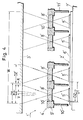
- FIG 4 shows an optical reader to which the present invention may be also applied.
- the optical reader 1' comprises a reading head 2' disposed in parallel to an image surface 3' to be detected.
- a lens system 4' retained by a lens holder 9' is arranged between the reading head and the image surface.
- the reading head 2' includes a plurality (e.g. 16) of sensor array chips 5' arranged in a longitudinal row on a substrate 6' as constantly spaced from each other.
- Each sensor array chip comprises a plurality (e.g. 64 or 128) of light receiving elements, such as phototransistors, arranged at constant minute spacing in an array on a unit wafer which may be diced from a longer wafer.
- the lens holder 9' having lens holding bores 10' and light shielding partition walls 11' retains aspheric convex lenses 8' in exactly corresponding relation to the respective array chips 5'.
- the arrangement and magnification of the lens system 4' may be determined in relation to the chips 5' and the image surface 3' in substantially the same manner as previously described in connection with the optical printer 1 ( Figure 1). However, it should be appreciated here that the image surface 3' is located at the object point of each lens 8', whereas each chip 5' is located at the image point. Thus, an image on the surface 3' is reduced when recognized by the sensor chips 5'.
- the image surface 3' provides an overall effective width W which is divided into unit array width portions D2' corresponding in number to the sensor array chips 5', a constant spacing X being formed between each two adjacent unit array width portions D2'. Further, each unit width portion D2' is equally subdivided into picture element width portions corresponding in number to the light receiving elements of each sensor array chip 5'. The pitch Y between each two adjacent picture element width portions is equal to the spacing X described above.
- the image reduction provided by each convex lens 8' is such that the distance between the two farthest picture element width portions within each unit array width portion exactly corresponds to the distance between the two farthest light receiving elements within each sensor array chip 5'.
- the entirety of an image or images contained within the overall effective width W can be scanned at constant minute pitch Y (equal to X) by the photosensors of the respective chips 5' even if the chips are longitudinally spaced as illustrated.
- the convex lens system 4, 4' serves to form an inverted image with respect to each of the respective array chips 5, 5'.
- serial data or signals to each chip 5, 5' in reverse order.
- Such reverse data feeding will be explained hereinafter in connection with the optical printer.
- the convex lenses 8, 8' are all separate and individually retained in place by the lens holder 9.
- a single lens array plate having a required number of integral lens portions may be used.
- a plurality of lens array plates each having a plurality of integral lens portions may be used in combination to provide a required number of lens portions.
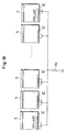
- lens array plate 13 In Figures 5 and 6, there is shown an example of lens array plate 13.
- the lens array plate is generally rectangular in plan view, and has four integral lens portions 13a which are also rectangular in plan view.
- the lens portions 13a are shown as distinctly spaced longitudinally of the plate.
- the lens array plate further has a pair of longitudinal margins 13b which are used for mounting purposes, as described later.
- the lens array plate is made of a plastic.
- lens array plates 13 In assembly, four of such lens array plates 13 for example are used in combination to provide sixteen lens portions 13a in total.
- the lens array plate may be modified to have sixteen integral lens portions.
- the use of such a lens array plate or plates simplifies the construction, and facilitates assembly.
- Figures 7 and 8 show another lens array plate 14 which has three integral lens portions 14a, and a pair of longitudinal margins 14b for mounting purposes. As opposed to the example shown in Figure 5, the lens portions 14a have round configuration in plan view, and merges with each other.
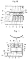
- the lens array plate or plates 13 (or 14) described above may be advantageously held in place by an elongate lens holder or housing 9'' shown in Figures 9 to 11. More specifically, the lens holder 9'' has an upper longitudinal opening 15 which is rectangular in plan view. The longitudinal opening 15 is formed with a pair of longitudinal grooves 15a for receiving the longitudinal margins 13b of the lens array plate 13.
- the lens array plate or a terminal lens array plate has an elongated end portion 13c which is anchored in a corresponding transverse groove 17 at each end of the holder. Thus, the lens array plate is prevented from displacing in any direction relative to the lens holder.
- a transparent guard plate 18 which is preferably made of an acrylic resin.
- the guard plate may be mounted to the lens holder 9'' in a manner similar to the lens array plate.
- the guard plate serves to prevent entry of foreign substances such as dust, thereby protecting the lens array plate and other important components against contamination and damages.
- the lens holder 9'' has a lower interior space 19 defined by a pair of longitudinal walls 12'' and a pair of end walls 9a (only one shown).
- the interior space is separated by a plurality of light shielding partition walls 11'' extending transversely of the holder. These partition walls serve to prevent undesirable light leakage, as already described.
- the end walls 9a of the lens holder 9'' are shown to be supported on the heat sink 7 of the LED print head 2.
- Indicated at 20 is a printed circuit board, and at 21 an electrical connector.
- the lens holder 9'' may be made of a synthetic resin, whereas the heat sink may be made of a heat conducting metal such as aluminum.
- the holder may also be made of a metal such as aluminum, thereby assisting heat dissipation provided by the heat sink.
- Figures 12 to 14 show a conductor arrangement on the substrate 6.
- the conductor arrangement includes a common cathode strip 22 formed at each end with a terminal lead 22a for grounding.
- Each LED array chip 5 incorporating an array of light emitting diodes is mounted on the cathode strip 22 with the cathode of each diode held in conduction therewith.
- the chip carries anode pads 23 disposed in a staggered arrangement on both sides of the diode array, each pad being held in conduction with the anode of a corresponding diode. Such a staggered arrangement of the anode pads are necessary because the diode array density is very high.
- the conductor arrangement further includes a pattern of anode leads 24 extending on the substrate 6 for connection to relevant control circuits IC ( Figure 12) which are provided for separately driving the respective array chips 5.
- the anode leads have enlarged connection ends 24a located on both sides of the cathode strip 22.
- a half number of the anode leads must extend under and across the cathode strip 22 with an insulation layer 25 interposed between the cathode strip and the anode leads, as better illustrated in Figure 14.
- the connection ends of the anode leads are connected to the respective anode pads 23 through wires 26.
- the common cathode strip 22 must be made long when a large number of LED array chips are used to provide a large printing width. If the cathode strip 22 has no auxiliary grounding lead, the internal resistance of the cathode strip becomes non-negligible with respect to those array chips 5 which are located away from the terminal grounding lead 22a. In some cases, the intermediately positioned array chips may suffer a brightness drop of 10-20% due to the increased internal resistance of the cathode strip.
- auxiliary cathode leads 22b serve to prevent a brightness drop with respect to all array chips 5 by separately grounding them though shortest possible paths. If desired, such an auxiliary cathode lead may be provided only with respect to one array chip 5 which is located farthest from the terminal cathode lead 22a.
- each lens 8 forms an inverted image, on the photosensitive drum 3, of the luminescent dot arrangement of a corresponding LED array chip 5.
- a first solution is to feed serial control signals in reverse order to each control circuit IC ( Figure 12).
- a second solution is to feed serial control signals in normal order to the control circuit wherein the signal series is registered in reverse order.
- Figure 15 illustrates the second solution.
- each LED array chip 5 is shown to incorporate an array of light emitting diodes L1-L64.
- Each control circuit IC comprises a shift register SR, a latch circuit LA and a drive circuit DR.
- the shift register SR has memory cells corresponding in number to the diodes of the chip for receiving a relevant series of data.
- the latch circuit LA has latch cells for parallel latching of the registered serial data upon reception of a latch signal.
- the drive circuit DR which is connected to the anodes of the respective diodes L1-L64 via the anode leads 24, functions to supply the latched data to the diodes upon reception of a strobe signal.
- each shift register SR is oriented reversely to the data transmitting direction between each two adjacent shift registers, so that the serial data supplied in normal order are registered in reverse order. More specifically, the data transmission between the two adjacent shift registers SR occurs in the rightward direction in Figure 15, whereas the data shifting within the single shift register SR occurs in the leftward direction.
- the last memory cell (numbered 64) of the first shift register (the lefthand register in Figure 15) is connected in series to the first cell (numbered 1) of the second shift register, and the last cell of the second shift register is connected in series to the first cell of the third shift register, such connection being repeated up to the last shift register (not shown).
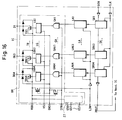
- Figure 16 illustrates a more specific circuit arrangement for each control circuit IC.
- the shift register SR of the control circuit is again shown to include memory cells SR1-SR64 arranged to store, in reverse order, the serial data supplied in normal order though a data input terminal DIN, as previously described.
- the latch circuit LA includes latch cells LA1-LA64 for parallel latching of the registered data of the shift register upon feeding of a latch signal through a latch terminal LIN. It should be noted that the memorized or latched data are "1" for those cells corresponding to the LEDs ( Figure 15) to be lit, whereas the data are "0" for those cells corresponding to the LEDs not to be lit.
- control circuit DR includes a gate circuit GA, a logic circuit LG, a drive transistor circuit TR, and a gate voltage setting circuit 27.
- the gate circuit GA comprises AND gates GA1-GA64. When a strobe signal is fed through a strobe terminal STR, each AND gate produces a high or low output "1" or “0” depending respectively on the "1” or “0” state of the corresponding latch cell.
- the logic circuit LG incorporates logic gates LG1-LG64, whereas the drive transistor circuit comprises MOSFETs (metal oxide semiconductor field effect transistor) TR1-TR64 whose output terminals D1-D64 are connected to the respective LEDs L1-L64 ( Figure 15).
- Each logic gate functions to apply a gate voltage VG to the gate of the corresponding MOSFET in response to the "1" output from the corresponding AND gate.
- a voltage equal to a difference between the gate voltage VG and a source voltage VDD is applied across the MOSFET for activation thereof, thereby lighting the corresponding LED L1-L64 ( Figure 15) for intended printing.
- a voltage equivalent to the source voltage VDD is produced by the logic gate in response to the "0" output from the AND gate, so that the MOSFET remains inactive.
- a conventional way for such voltage adjustment is to provide a voltage dividing circuit arranged outside each control circuit IC for applying an adjusted gate voltage. More specifically, the voltage dividing circuit enables voltage adjustment through changing the voltage division ratio by selecting resistors to be incorporated into the circuit.
- this manner of voltage adjustment it is difficult to minutely adjust the gate voltage because there is a limitation on the kinds of available resistors. Further, this manner of voltage adjustment is time-taking.
- the gate voltage setting circuit 27 incorporated into the drive circuit DR of each control circuit enables minute voltage adjustment with ease.
- Figure 17 represents the detailed arrangement of the gate voltage setting circuit.
- the gate voltage setting circuit 27 comprises a first group of series resistors Ra, Rb, and a second group of parallel resistors R1-R7.
- the resistor Ra in the first group is connected to the voltage source VDD, and an intermediate position between the two resistors Ra, Rb is connected to a terminal GS0.
- the resistors R1-R7 in the second group are connected commonly to the resistor Rb in the first group, but separately to grounding terminals GS1-GS7.
- the connection between the first resistor group and the second resistor group is further connected to the gate voltage supply terminal VG. Assuming now that the resistivity of the resistor R1 is taken as R (i.e.
- R1 R
- the relative resistivities of the respective resitors may be set as follows.
- R1 1.0R
- R4 2.8R
- R5 3.4R
- grounding terminals GS1-GS7 are commonly grounded through a common grounding resistor Rc, as illustrated in Figure 17.
- the gate voltage terminal VG is connected to the gate input of each logic gate LG1-LG64.
- the gate voltage VG is determined by voltage division of the source voltage VDD which is provided by the first group resistors Ra, Rb, the selected three of the second group resistors R1-R7, and the common grounding resistor Rc.
- the second group resistors R1-R7, seven according to the illustrated example, provide various combinations (thirty five combinations) for selecting three of them.
- the gate voltage setting circuit 27 utilizes only a limited number of second group resistors in an identical arrangement for each control circuit, but yet provides various resistor combinations to enable minute voltage adjustment. Hence, this is much more advantageous than the prior art which requires various kinds of resistors for intended adjustment.
- Figure 18 shows an example wherein differently selected three of the grounding terminals GS1-GS7 of the respective control circuits IC are connected to the common grounding resistor Rc. In this way, the associated LED array chips 5 are controlled so that the average brightness of each array chip is maintained within a limited range.
- Figure 19 shows a diagram which represents the achievable range of the gate voltage VG by various combinations of three grounding terminals when the voltage across the common grounding resistor Rc ( Figure 17) is set at 0.5V.
- the curve A indicates various gate voltages available when only the resistor Ra of the first group is made effective, that is, when the terminal GS0 is shorted to the gate voltage terminal VG.
- the curve B indicates various gate voltages obtainable when the two resistors Ra, Rb of the first group are made effective. It is understood from Figure 19 that the gate voltage VG may be varied or adjusted minutely within a wide range of 1.90-2.90V.
- the second resistor group of the gate voltage setting circuit 27 may include more or less than seven parallel resistors. Further, any number of the second group resistors R1-R7 may be selected to increase the range of gate voltage adjustment.
- each logic gate LG1-LG64 is shown to include a pair of MOS field effect transistors Ta, Tb which are opposite in polarity.
- One transistor Ta is activated to supply the source voltage VDD to the corresponding MOSFET TR1-TR64 of the drive transistor circuit when the signal from the corresponding AND gate GA1-GA64 is high.
- the other transistor Tb is activated to supply the gate voltage VG when the signal from the AND gate is low.
Landscapes
- Engineering & Computer Science (AREA)
- Multimedia (AREA)
- Physics & Mathematics (AREA)
- Signal Processing (AREA)
- Optics & Photonics (AREA)
- General Physics & Mathematics (AREA)
- General Engineering & Computer Science (AREA)
- Theoretical Computer Science (AREA)
- Health & Medical Sciences (AREA)
- General Health & Medical Sciences (AREA)
- Toxicology (AREA)
- Printers Or Recording Devices Using Electromagnetic And Radiation Means (AREA)
- Facsimile Heads (AREA)
- Dot-Matrix Printers And Others (AREA)
Applications Claiming Priority (11)
| Application Number | Priority Date | Filing Date | Title |
|---|---|---|---|
| JP152582/88 | 1988-06-21 | ||
| JP15258288A JP2510423B2 (ja) | 1988-06-21 | 1988-06-21 | 光情報書込み装置および光情報検出装置ならびにその光学レンズ系の構造 |
| JP63171482A JPH0220360A (ja) | 1988-07-08 | 1988-07-08 | Ledプリントヘッド |
| JP171483/88 | 1988-07-08 | ||
| JP63171483A JPH0220361A (ja) | 1988-07-08 | 1988-07-08 | Ledプリントヘッド |
| JP17148488A JPH0696295B2 (ja) | 1988-07-08 | 1988-07-08 | Ledプリントヘッド |
| JP171482/88 | 1988-07-08 | ||
| JP171484/88 | 1988-07-08 | ||
| JP96705/88U | 1988-07-21 | ||
| JP1988096705U JPH079394Y2 (ja) | 1988-07-21 | 1988-07-21 | 発光素子駆動用の集積回路装置 |
| EP19890201634 EP0348003A3 (de) | 1988-06-21 | 1989-06-20 | Gerät zur optischen Informationszeichnung |
Related Parent Applications (2)
| Application Number | Title | Priority Date | Filing Date |
|---|---|---|---|
| EP89201634.6 Division | 1989-06-20 | ||
| EP19890201634 Division EP0348003A3 (de) | 1988-06-21 | 1989-06-20 | Gerät zur optischen Informationszeichnung |
Publications (2)
| Publication Number | Publication Date |
|---|---|
| EP0600853A2 true EP0600853A2 (de) | 1994-06-08 |
| EP0600853A3 EP0600853A3 (en) | 1994-07-06 |
Family
ID=27525808
Family Applications (2)
| Application Number | Title | Priority Date | Filing Date |
|---|---|---|---|
| EP19890201634 Withdrawn EP0348003A3 (de) | 1988-06-21 | 1989-06-20 | Gerät zur optischen Informationszeichnung |
| EP19940200320 Ceased EP0600853A3 (en) | 1988-06-21 | 1989-06-20 | Apparatus for optically writing information. |
Family Applications Before (1)
| Application Number | Title | Priority Date | Filing Date |
|---|---|---|---|
| EP19890201634 Withdrawn EP0348003A3 (de) | 1988-06-21 | 1989-06-20 | Gerät zur optischen Informationszeichnung |
Country Status (4)
| Country | Link |
|---|---|
| US (1) | US5023442A (de) |
| EP (2) | EP0348003A3 (de) |
| CA (1) | CA1334726C (de) |
| DK (1) | DK300689A (de) |
Families Citing this family (57)
| Publication number | Priority date | Publication date | Assignee | Title |
|---|---|---|---|---|
| JPH02201386A (ja) * | 1989-01-30 | 1990-08-09 | Canon Inc | 画像記録装置 |
| US4991949A (en) * | 1990-01-23 | 1991-02-12 | Comar, Inc. | Dust protection device for an image sensor |
| US5325207A (en) * | 1991-04-29 | 1994-06-28 | Westinghouse Electric Corp. | Facsimile machine using thin film electroluminescent device for spot scanning |
| EP0547495B1 (de) * | 1991-12-19 | 1997-08-20 | Sharp Kabushiki Kaisha | Bilderzeugungsgerät |
| JPH05183679A (ja) * | 1991-12-26 | 1993-07-23 | Kyocera Corp | 原稿読み取り装置 |
| US5444520A (en) * | 1993-05-17 | 1995-08-22 | Kyocera Corporation | Image devices |
| US5617131A (en) * | 1993-10-28 | 1997-04-01 | Kyocera Corporation | Image device having a spacer with image arrays disposed in holes thereof |
| US5655189A (en) * | 1994-05-27 | 1997-08-05 | Kyocera Corporation | Image device having thermally stable light emitting/receiving arrays and opposing lenses |
| US6330017B1 (en) * | 1994-10-12 | 2001-12-11 | Ricoh Co., Ltd. | Light emitting diode array head including focusing lenses |
| DE19545484C2 (de) * | 1995-12-06 | 2002-06-20 | Deutsche Telekom Ag | Bildaufnahmeeinrichtung |
| JP3732326B2 (ja) * | 1998-02-02 | 2006-01-05 | 株式会社沖データ | 光プリントヘッド |
| JPH11354271A (ja) * | 1998-06-05 | 1999-12-24 | Canon Inc | 感光材料書込み装置 |
| US6466245B1 (en) * | 1999-07-14 | 2002-10-15 | Canon Kabushiki Kaisha | Rod lens array and optical printer head and optical printer using the same |
| US6483101B1 (en) * | 1999-12-08 | 2002-11-19 | Amkor Technology, Inc. | Molded image sensor package having lens holder |
| US6483030B1 (en) * | 1999-12-08 | 2002-11-19 | Amkor Technology, Inc. | Snap lid image sensor package |
| JP2001343506A (ja) * | 2000-06-01 | 2001-12-14 | Rohm Co Ltd | レンズアレイの製造方法、レンズアレイおよびレンズアレイの遮光処理方法 |
| US7059040B1 (en) | 2001-01-16 | 2006-06-13 | Amkor Technology, Inc. | Optical module with lens integral holder fabrication method |
| KR100401020B1 (ko) * | 2001-03-09 | 2003-10-08 | 앰코 테크놀로지 코리아 주식회사 | 반도체칩의 스택킹 구조 및 이를 이용한 반도체패키지 |
| US7170660B2 (en) * | 2001-04-24 | 2007-01-30 | Ricoh Company, Ltd. | Optical scanner and image forming device |
| US7146106B2 (en) * | 2002-08-23 | 2006-12-05 | Amkor Technology, Inc. | Optic semiconductor module and manufacturing method |
| KR20070096020A (ko) * | 2002-09-17 | 2007-10-01 | 앤터온 비.브이. | 카메라 디바이스, 카메라 디바이스 제조 방법, 웨이퍼스케일 패키지 및 광학 어셈블리 |
| US20050093965A1 (en) * | 2003-11-04 | 2005-05-05 | Eastman Kodak Company | Multichannel printhead for photosensitive media |
| US20060261458A1 (en) * | 2003-11-12 | 2006-11-23 | Amkor Technology, Inc. | Semiconductor package and manufacturing method thereof |
| US7359579B1 (en) | 2004-10-08 | 2008-04-15 | Amkor Technology, Inc. | Image sensor package and its manufacturing method |
| JP4546285B2 (ja) * | 2005-02-28 | 2010-09-15 | 株式会社セイコーアイ・インフォテック | 光プリンタヘッドおよび画像形成装置 |
| US20070210246A1 (en) * | 2005-04-14 | 2007-09-13 | Amkor Technology, Inc. | Stacked image sensor optical module and fabrication method |
| US7227236B1 (en) | 2005-04-26 | 2007-06-05 | Amkor Technology, Inc. | Image sensor package and its manufacturing method |
| US20070272827A1 (en) * | 2005-04-27 | 2007-11-29 | Amkor Technology, Inc. | Image sensor package having mount holder attached to image sensor die |
| US7576401B1 (en) | 2005-07-07 | 2009-08-18 | Amkor Technology, Inc. | Direct glass attached on die optical module |
| US20080237824A1 (en) * | 2006-02-17 | 2008-10-02 | Amkor Technology, Inc. | Stacked electronic component package having single-sided film spacer |
| US7675180B1 (en) | 2006-02-17 | 2010-03-09 | Amkor Technology, Inc. | Stacked electronic component package having film-on-wire spacer |
| US7733364B2 (en) * | 2006-03-10 | 2010-06-08 | Seiko Epson Corporation | Line head and an image forming apparatus using such a line head |
| US7633144B1 (en) | 2006-05-24 | 2009-12-15 | Amkor Technology, Inc. | Semiconductor package |
| US20080030566A1 (en) * | 2006-08-04 | 2008-02-07 | Seiko Epson Corporation | Line Head and Image Forming Apparatus Using the Same |
| EP1905602A3 (de) | 2006-09-28 | 2008-05-14 | Oki Data Corporation | Linsenmatrix, Belichtungsvorrichtung, Bilderzeugungsvorrichtung und Lesevorrichtung |
| US7995085B2 (en) | 2007-07-04 | 2011-08-09 | Seiko Epson Corporation | Line head, and an image forming apparatus using the line head |
| US7764429B2 (en) | 2007-07-06 | 2010-07-27 | Seiko Epson Corporation | Lens array, A line head and an image forming apparatus using the line head |
| US7746369B2 (en) | 2007-07-06 | 2010-06-29 | Seiko Epson Corporation | Lens array, a line head and an image forming apparatus using the line head |
| US20090041504A1 (en) * | 2007-08-07 | 2009-02-12 | Seiko Epson Corporation | Light Exposure Head and Image Formation Apparatus Using the Same |
| US8120635B2 (en) * | 2008-01-18 | 2012-02-21 | Seiko Epson Corporation | Exposure head and an image forming apparatus |
| US20090185828A1 (en) * | 2008-01-18 | 2009-07-23 | Seiko Epson Corporation | Lens Array, Exposure Head, and Image Forming Apparatus |
| JP2009202574A (ja) * | 2008-01-28 | 2009-09-10 | Seiko Epson Corp | レンズアレイ、露光ヘッドおよび画像形成装置 |
| JP2009216730A (ja) * | 2008-03-06 | 2009-09-24 | Oki Data Corp | 露光装置、画像形成装置及び読取装置 |
| JP2010162850A (ja) * | 2009-01-19 | 2010-07-29 | Seiko Epson Corp | ラインヘッドおよび画像形成装置 |
| JP2010167679A (ja) * | 2009-01-22 | 2010-08-05 | Seiko Epson Corp | ラインヘッドおよび画像形成装置 |
| JP2010184392A (ja) * | 2009-02-10 | 2010-08-26 | Seiko Epson Corp | ラインヘッドおよび画像形成装置 |
| JP2010188528A (ja) * | 2009-02-13 | 2010-09-02 | Seiko Epson Corp | ラインヘッドおよび画像形成装置 |
| JP2010194764A (ja) * | 2009-02-23 | 2010-09-09 | Seiko Epson Corp | ラインヘッドおよび画像形成装置 |
| KR101728464B1 (ko) * | 2010-05-11 | 2017-04-19 | 에스프린팅솔루션 주식회사 | 렌즈 어레이, 선형 노광 장치 및 선형 노광 장치를 채용한 광학 장치 |
| JP2012174810A (ja) * | 2011-02-18 | 2012-09-10 | Fuji Xerox Co Ltd | 発光部品、プリントヘッドおよび画像形成装置 |
| US9627572B2 (en) | 2012-04-25 | 2017-04-18 | Kyocera Corporation | Light receiving and emitting element module and sensor device using same |
| WO2016052599A1 (ja) * | 2014-09-30 | 2016-04-07 | 積水化学工業株式会社 | 電子機器用熱伝導性発泡体シート |
| JP6008218B1 (ja) * | 2015-03-30 | 2016-10-19 | ウシオ電機株式会社 | 光源装置 |
| US9780133B2 (en) * | 2015-08-04 | 2017-10-03 | Creative Sensor Inc. | Wafer-level lens structure for contact image sensor module |
| JP2017128045A (ja) * | 2016-01-20 | 2017-07-27 | 株式会社沖データ | 露光装置、画像形成ユニットおよび画像形成装置 |
| US10606092B1 (en) * | 2016-03-21 | 2020-03-31 | Mark Lauer | Integral imaging system with array of horizontally elongate rectangular microlenses |
| US10204947B2 (en) * | 2016-09-09 | 2019-02-12 | Omnivision Technologies, Inc. | Cover-glass-free array camera with individually light-shielded cameras |
Family Cites Families (12)
| Publication number | Priority date | Publication date | Assignee | Title |
|---|---|---|---|---|
| US4114037A (en) * | 1977-05-16 | 1978-09-12 | Northern Telecom Limited | Multiple lens system for an optical imaging device |
| US4432022A (en) * | 1980-04-14 | 1984-02-14 | Canon Kabushiki Kaisha | Original reading apparatus |
| US4539482A (en) * | 1980-10-09 | 1985-09-03 | Canon Kabushiki Kaisha | Reading apparatus |
| DE3224356A1 (de) * | 1982-06-30 | 1984-01-12 | Philips Patentverwaltung Gmbh, 2000 Hamburg | Optischer drucker mit lichtschaltelementen |
| JPH0626420B2 (ja) * | 1983-01-24 | 1994-04-06 | キヤノン株式会社 | 光センサアレイ装置 |
| US4550249A (en) * | 1983-04-21 | 1985-10-29 | At&T Bell Laboratories | Optical disc read/write apparatus |
| JPS6015622A (ja) * | 1983-07-08 | 1985-01-26 | Fuji Xerox Co Ltd | 光情報の書込み装置 |
| JPS6262322A (ja) * | 1985-09-12 | 1987-03-19 | Rohm Co Ltd | 光プリンタ |
| US4639127A (en) * | 1985-12-10 | 1987-01-27 | Itt Corporation | Exposure apparatus for printing system |
| EP0228023B1 (de) * | 1985-12-27 | 1993-06-02 | Kabushiki Kaisha Toshiba | Festkörperbildsensor mit amorpher, halbleitender, photoleitender Zellenmatrix |
| JP2816147B2 (ja) * | 1987-03-27 | 1998-10-27 | 株式会社日立製作所 | 発光ダイオードアレイ用駆動回路 |
| JP3134933B2 (ja) * | 1987-04-01 | 2001-02-13 | ネックスプレス・ソリューションズ・エルエルシー | プリンタ装置 |
-
1989
- 1989-06-19 US US07/367,750 patent/US5023442A/en not_active Expired - Lifetime
- 1989-06-19 DK DK300689A patent/DK300689A/da not_active Application Discontinuation
- 1989-06-20 EP EP19890201634 patent/EP0348003A3/de not_active Withdrawn
- 1989-06-20 EP EP19940200320 patent/EP0600853A3/en not_active Ceased
- 1989-06-20 CA CA000603344A patent/CA1334726C/en not_active Expired - Fee Related
Also Published As
| Publication number | Publication date |
|---|---|
| EP0348003A3 (de) | 1991-09-25 |
| CA1334726C (en) | 1995-03-14 |
| DK300689A (da) | 1989-12-22 |
| EP0348003A2 (de) | 1989-12-27 |
| US5023442A (en) | 1991-06-11 |
| DK300689D0 (da) | 1989-06-19 |
| EP0600853A3 (en) | 1994-07-06 |
Similar Documents
| Publication | Publication Date | Title |
|---|---|---|
| EP0600853A2 (de) | Gerät zum optischen Schreiben von Information | |
| US5150016A (en) | LED light source with easily adjustable luminous energy | |
| EP0098382B1 (de) | Gleichmässig intensive Belichtung mittels einer dicht zusammengefassten Linsenreihe | |
| US4706130A (en) | Image recording apparatus utilizing light emitting diodes with pixel shape correction | |
| US6163036A (en) | Light emitting element module with a parallelogram-shaped chip and a staggered chip array | |
| US4734714A (en) | Optical print head with LED diode array | |
| JPWO1986002045A1 (ja) | 光学印字装置用の光学印字ヘッド | |
| US5946022A (en) | LED head | |
| GB2099221A (en) | Light emitting diode array devices and image transfer systems | |
| KR100359638B1 (ko) | 화상처리장치 | |
| EP1109396A1 (de) | Integrierter bildlese/schreibkopf, sowie bildprozessor mit schreiblesekopf | |
| KR100781910B1 (ko) | 광 프린터 헤드의 점등 방법 | |
| EP2178120A2 (de) | Driverschaltung, optischer Druckkopf und Bilderzeugungsvorrichtung | |
| JP2845719B2 (ja) | ドライバic | |
| US4361844A (en) | Recording head | |
| US6611280B1 (en) | Flexible cable, flexible cable mount method, semiconductor device with flexible cable, led array head with flexible cable, image forming apparatus with such led array head | |
| EP0507366B1 (de) | LED-Belichtungskopf | |
| US4998119A (en) | Multiplexed light emitting diode printhead | |
| KR100453730B1 (ko) | 선형광원 및 이를 구비한 화상판독장치 | |
| US6285047B1 (en) | Linear image sensor device, IC assembling substrate and method for assembling the same | |
| KR940009023B1 (ko) | 발광다이오드 프린트 헤드 | |
| EP0449588B1 (de) | Methode zum Betreiben eines optischen Sensors vom Dünnschichttransistor-Typ und seine Treibereinheit | |
| JPH02212167A (ja) | Ledプリントヘッド | |
| US5034757A (en) | LED printing array current control | |
| JP3595044B2 (ja) | 自己走査型発光装置およびこれを用いた光プリンタ装置 |
Legal Events
| Date | Code | Title | Description |
|---|---|---|---|
| PUAI | Public reference made under article 153(3) epc to a published international application that has entered the european phase |
Free format text: ORIGINAL CODE: 0009012 |
|
| PUAL | Search report despatched |
Free format text: ORIGINAL CODE: 0009013 |
|
| 17P | Request for examination filed |
Effective date: 19940209 |
|
| AC | Divisional application: reference to earlier application |
Ref document number: 348003 Country of ref document: EP |
|
| AK | Designated contracting states |
Kind code of ref document: A2 Designated state(s): DE FR GB IT NL |
|
| AK | Designated contracting states |
Kind code of ref document: A3 Designated state(s): DE FR GB IT NL |
|
| 17Q | First examination report despatched |
Effective date: 19960312 |
|
| APAB | Appeal dossier modified |
Free format text: ORIGINAL CODE: EPIDOS NOAPE |
|
| APAD | Appeal reference recorded |
Free format text: ORIGINAL CODE: EPIDOS REFNE |
|
| APAB | Appeal dossier modified |
Free format text: ORIGINAL CODE: EPIDOS NOAPE |
|
| STAA | Information on the status of an ep patent application or granted ep patent |
Free format text: STATUS: THE APPLICATION HAS BEEN REFUSED |
|
| 18R | Application refused |
Effective date: 19960823 |
|
| APAF | Appeal reference modified |
Free format text: ORIGINAL CODE: EPIDOSCREFNE |