EP0595561A1 - Amplificateurs - Google Patents
Amplificateurs Download PDFInfo
- Publication number
- EP0595561A1 EP0595561A1 EP93308438A EP93308438A EP0595561A1 EP 0595561 A1 EP0595561 A1 EP 0595561A1 EP 93308438 A EP93308438 A EP 93308438A EP 93308438 A EP93308438 A EP 93308438A EP 0595561 A1 EP0595561 A1 EP 0595561A1
- Authority
- EP
- European Patent Office
- Prior art keywords
- amplifier stage
- inductive
- output
- frequencies
- capacitive feedback
- Prior art date
- Legal status (The legal status is an assumption and is not a legal conclusion. Google has not performed a legal analysis and makes no representation as to the accuracy of the status listed.)
- Granted
Links
- 230000001939 inductive effect Effects 0.000 claims abstract description 18
- 239000003990 capacitor Substances 0.000 description 5
- 230000006835 compression Effects 0.000 description 1
- 238000007906 compression Methods 0.000 description 1
- 238000007796 conventional method Methods 0.000 description 1
- 230000001419 dependent effect Effects 0.000 description 1
- 230000000694 effects Effects 0.000 description 1
- 230000002452 interceptive effect Effects 0.000 description 1
- 230000003071 parasitic effect Effects 0.000 description 1
- 230000010363 phase shift Effects 0.000 description 1
- 230000000717 retained effect Effects 0.000 description 1
Images
Classifications
-
- H—ELECTRICITY
- H03—ELECTRONIC CIRCUITRY
- H03F—AMPLIFIERS
- H03F1/00—Details of amplifiers with only discharge tubes, only semiconductor devices or only unspecified devices as amplifying elements
- H03F1/34—Negative-feedback-circuit arrangements with or without positive feedback
-
- H—ELECTRICITY
- H03—ELECTRONIC CIRCUITRY
- H03F—AMPLIFIERS
- H03F3/00—Amplifiers with only discharge tubes or only semiconductor devices as amplifying elements
- H03F3/189—High-frequency amplifiers, e.g. radio frequency amplifiers
- H03F3/19—High-frequency amplifiers, e.g. radio frequency amplifiers with semiconductor devices only
- H03F3/191—Tuned amplifiers
-
- H—ELECTRICITY
- H03—ELECTRONIC CIRCUITRY
- H03F—AMPLIFIERS
- H03F2200/00—Indexing scheme relating to amplifiers
- H03F2200/372—Noise reduction and elimination in amplifier
-
- H—ELECTRICITY
- H03—ELECTRONIC CIRCUITRY
- H03F—AMPLIFIERS
- H03F2203/00—Indexing scheme relating to amplifiers with only discharge tubes or only semiconductor devices as amplifying elements covered by H03F3/00
- H03F2203/45—Indexing scheme relating to differential amplifiers
- H03F2203/45316—Indexing scheme relating to differential amplifiers the AAC comprising one or more discrete inductive elements or coils
-
- H—ELECTRICITY
- H03—ELECTRONIC CIRCUITRY
- H03F—AMPLIFIERS
- H03F2203/00—Indexing scheme relating to amplifiers with only discharge tubes or only semiconductor devices as amplifying elements covered by H03F3/00
- H03F2203/45—Indexing scheme relating to differential amplifiers
- H03F2203/45546—Indexing scheme relating to differential amplifiers the IC comprising one or more capacitors feedback coupled to the IC
-
- H—ELECTRICITY
- H03—ELECTRONIC CIRCUITRY
- H03F—AMPLIFIERS
- H03F2203/00—Indexing scheme relating to amplifiers with only discharge tubes or only semiconductor devices as amplifying elements covered by H03F3/00
- H03F2203/45—Indexing scheme relating to differential amplifiers
- H03F2203/45638—Indexing scheme relating to differential amplifiers the LC comprising one or more coils
Definitions
- the present invention relates to amplifiers, and in particular although not exclusively to low-noise radio frequency amplifiers.
- Adjacent channel rejection is conventionally achieved in the IF filters of a receiver, so that any front-end amplifying stage, prior to the first frequency changer, may have to cope with large adjacent-channel signals and at the same time introduce the minimum possible level of noise.
- front-end amplifying stages were perfectly linear they would be able to cope with any level of adjacent-channel signal.
- stages are not perfectly linear, and can give rise to intermodulation products that may fall within the wanted channel, contributing to the noise and interfering with the reception of weak signals in the wanted channel.
- amplifier stages are also limited by the maximum signal level that can be handled without compression or clipping occurring.
- a low noise amplifier stage is provided with capacitive feedback, the value of capacitance at the output of said amplifier stage, including that presented by said capacitive feedback, being tuned with inductive load means to be substantially resonant at the range of frequencies to be amplified.
- a low noise transistor amplifier stage comprises a junction transistor having inductive collector load means and capacitive feedback means connected between output and input circuits thereof, the value of capacitance at the output of said amplifier stage, including that presented by said capacitive feedback, being substantially resonant with said inductive load means at the range of frequencies to be amplified.
- a differential input/differential output amplifier stage comprises a pair of junction transistors having their emitter electrodes connected to a common current source by way of respective inductive impedance elements and their collector electrodes connected to respective inductive loads, and respective capacitive feedback means connecting the collector circuits of said transistors to their respective base circuits, the values of capacitance at the outputs of said amplifier stage, including that presented by said feedback means, being arranged to be substantially resonant with said inductive loads at the range of frequencies to be amplified.
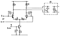
- a low-noise radio frequency amplifier stage in accordance with the present invention will now be described by way of example with reference to the accompanying drawing, which shows the amplifier stage diagrammatically.
- the amplifier stage comprises a pair of NPN junction transistors 1 and 2 the emitter electrodes of which are connected by way of respective inductive elements 3 and 4 to a common current source comprising a transistor 5, resistor 6 and capacitor 7, the value of current provided by said source being dependent upon the value of a bias signal applied to a terminal 8.
- Radio frequency input signals are applied by way of input terminals 9 and 10 to the base electrodes of the transistors 1 and 2, and output signals developed across inductive collector load impedances 11 and 12 are applied to a following stage 13 represented as a capacitive input impedance C IN and a current source 14.
- Capacitors 15 and 16 provide feedback from the collector circuits of the transistors 1 and 2 to their base circuits.
- the use of reactive components rather than resistive components to provide the feedback introduces much less noise and consequently little increase in the noise figure over that associated with the transistors themselves.
- the values of the reactive components are chosen so that the capacitances at the collector electrodes of the transistors 1 and 2, including the capacitance values presented by the capacitors 15 and 16, the collector capacitances of the transistors 1 and 2 and the input capacitance C IN of the following stage 13, are arranged to be resonant with the inductive load impedances 11 and 12 at the range of frequencies to be amplified.
- phase shifts introduced by the capacitors 15 and 16 and the inductive elements 3 and 4 are arranged to cancel, so that the input impedance presented at the terminals 9 and 10 is almost entirely resistive, and it is possible to define a low standing wave ratio real input impedance.
- the dominant parasitics of the transistors 1 and 2 are effectively in parallel with the respective capacitors 15 and 16 and are tuned out.
- the tuning of the output circuit with the capacitive input impedance of the following stage 13 achieves optimum power matching.
- the circuit therefore enables accurate input and output power matching, low noise figure and large signal handing with minimum power consumption.
Landscapes
- Engineering & Computer Science (AREA)
- Power Engineering (AREA)
- Amplifiers (AREA)
Applications Claiming Priority (2)
| Application Number | Priority Date | Filing Date | Title |
|---|---|---|---|
| GB9222449A GB2272121B (en) | 1992-10-26 | 1992-10-26 | Amplifiers |
| GB9222449 | 1992-10-26 |
Publications (2)
| Publication Number | Publication Date |
|---|---|
| EP0595561A1 true EP0595561A1 (fr) | 1994-05-04 |
| EP0595561B1 EP0595561B1 (fr) | 1998-12-23 |
Family
ID=10724051
Family Applications (1)
| Application Number | Title | Priority Date | Filing Date |
|---|---|---|---|
| EP93308438A Expired - Lifetime EP0595561B1 (fr) | 1992-10-26 | 1993-10-22 | Amplificateurs |
Country Status (5)
| Country | Link |
|---|---|
| US (1) | US5378997A (fr) |
| EP (1) | EP0595561B1 (fr) |
| JP (1) | JPH0715245A (fr) |
| DE (1) | DE69322737T2 (fr) |
| GB (1) | GB2272121B (fr) |
Cited By (1)
| Publication number | Priority date | Publication date | Assignee | Title |
|---|---|---|---|---|
| EP1575161A1 (fr) * | 2004-03-12 | 2005-09-14 | STMicroelectronics S.A. | Circuit de conversion d'un signal différentiel en un signal non différentiel, et émetteur RF doté d'un tel circuit |
Families Citing this family (13)
| Publication number | Priority date | Publication date | Assignee | Title |
|---|---|---|---|---|
| JPH1056336A (ja) * | 1996-08-09 | 1998-02-24 | Mitsubishi Electric Corp | ミキサ回路 |
| JPH10322135A (ja) * | 1997-05-21 | 1998-12-04 | Mitsubishi Electric Corp | ミキサ回路 |
| DE59811532D1 (de) * | 1997-09-11 | 2004-07-15 | Infineon Technologies Ag | Differenzverstärker |
| JP3386019B2 (ja) | 1999-10-27 | 2003-03-10 | 日本電気株式会社 | ミキサ回路 |
| US6351502B1 (en) * | 2000-01-13 | 2002-02-26 | Atheros Communications, Inc. | RF front-end with multistage stepdown filtering architecture |
| JP2006129444A (ja) * | 2004-09-30 | 2006-05-18 | Renesas Technology Corp | 高周波電力増幅器および高周波電力増幅器モジュール |
| CN1725630B (zh) * | 2005-07-15 | 2010-10-06 | 摩比天线技术(深圳)有限公司 | 低噪声放大器件模块装置 |
| KR100748721B1 (ko) * | 2006-06-15 | 2007-08-13 | 삼성전자주식회사 | 저잡음 증폭을 위한 푸시-풀 증폭기 및 방법 |
| JP5571732B2 (ja) * | 2012-04-17 | 2014-08-13 | 日本電信電話株式会社 | 差動増幅器 |
| JP2017509733A (ja) | 2014-01-08 | 2017-04-06 | アベリー・デニソン・コーポレイションAvery Dennison Corporation | 選択的に粘着性除去された接着剤を用いる品物、組成物、システム、及び方法 |
| JP6780226B2 (ja) * | 2015-08-11 | 2020-11-04 | 富士通株式会社 | 増幅回路及び送信装置 |
| CN105162422A (zh) * | 2015-09-07 | 2015-12-16 | 燕山大学 | 单端构造低噪声放大器 |
| WO2017147055A1 (fr) | 2016-02-22 | 2017-08-31 | Avery Dennison Corporation | Étiquette de contenu étendu transparente avec adhésif détackifié sélectivement |
Citations (4)
| Publication number | Priority date | Publication date | Assignee | Title |
|---|---|---|---|---|
| GB1147926A (en) * | 1967-01-27 | 1969-04-10 | Rca Corp | Parametric mode suppressor for transistor circuits |
| GB1241285A (en) * | 1970-02-02 | 1971-08-04 | Mullard Ltd | Improvements relating to neutralised transistor amplifiers |
| GB2225502A (en) * | 1988-11-02 | 1990-05-30 | Secr Defence | L.F. noise reduction using negative feedback |
| US5117203A (en) * | 1990-12-13 | 1992-05-26 | General Electric Company | Phase stable limiting power amplifier |
Family Cites Families (4)
| Publication number | Priority date | Publication date | Assignee | Title |
|---|---|---|---|---|
| US4287477A (en) * | 1979-02-22 | 1981-09-01 | Dynamic Compliance, Incorporated | Feedback arrangement |
| US4878033A (en) * | 1988-08-16 | 1989-10-31 | Hughes Aircraft Company | Low noise microwave amplifier having optimal stability, gain, and noise control |
| CA2003401C (fr) * | 1988-11-21 | 1994-03-15 | Noboru Ishihara | Circuit amplificateur a charge de reaction |
| US5172076A (en) * | 1992-03-26 | 1992-12-15 | Northern Telecom Limited | Resonant circuit formed of two amplifiers connected in a loop and multiple resonator circuits constructed therefrom |
-
1992
- 1992-10-26 GB GB9222449A patent/GB2272121B/en not_active Expired - Fee Related
-
1993
- 1993-10-20 US US08/139,436 patent/US5378997A/en not_active Expired - Lifetime
- 1993-10-22 DE DE69322737T patent/DE69322737T2/de not_active Expired - Fee Related
- 1993-10-22 EP EP93308438A patent/EP0595561B1/fr not_active Expired - Lifetime
- 1993-10-25 JP JP5288643A patent/JPH0715245A/ja not_active Ceased
Patent Citations (4)
| Publication number | Priority date | Publication date | Assignee | Title |
|---|---|---|---|---|
| GB1147926A (en) * | 1967-01-27 | 1969-04-10 | Rca Corp | Parametric mode suppressor for transistor circuits |
| GB1241285A (en) * | 1970-02-02 | 1971-08-04 | Mullard Ltd | Improvements relating to neutralised transistor amplifiers |
| GB2225502A (en) * | 1988-11-02 | 1990-05-30 | Secr Defence | L.F. noise reduction using negative feedback |
| US5117203A (en) * | 1990-12-13 | 1992-05-26 | General Electric Company | Phase stable limiting power amplifier |
Cited By (3)
| Publication number | Priority date | Publication date | Assignee | Title |
|---|---|---|---|---|
| EP1575161A1 (fr) * | 2004-03-12 | 2005-09-14 | STMicroelectronics S.A. | Circuit de conversion d'un signal différentiel en un signal non différentiel, et émetteur RF doté d'un tel circuit |
| FR2867632A1 (fr) * | 2004-03-12 | 2005-09-16 | St Microelectronics Sa | Circuit de conversion d'un signal differentiel en un signal non differentiel, et emetteur rf dote d'un tel circuit |
| US7525390B2 (en) | 2004-03-12 | 2009-04-28 | Stmicroelectronics S.A. | Circuit for converting a differential signal into a non-differential signal, and RF transmitter comprising such a circuit |
Also Published As
| Publication number | Publication date |
|---|---|
| GB2272121B (en) | 1996-03-27 |
| DE69322737D1 (de) | 1999-02-04 |
| GB2272121A (en) | 1994-05-04 |
| JPH0715245A (ja) | 1995-01-17 |
| EP0595561B1 (fr) | 1998-12-23 |
| GB9222449D0 (en) | 1992-12-09 |
| US5378997A (en) | 1995-01-03 |
| DE69322737T2 (de) | 1999-05-20 |
Similar Documents
| Publication | Publication Date | Title |
|---|---|---|
| EP0595561B1 (fr) | Amplificateurs | |
| US4559503A (en) | Amplifier for correcting group time delay of electrical signals and an intermediate frequency amplifier stage for radio equipment comprising an amplifier of this kind | |
| US4480337A (en) | Transistor mixer and amplifier input stage | |
| EP0915561B1 (fr) | Dispositifs mélangeurs de rejet de la fréquence-image | |
| US6882194B2 (en) | Class AB differential mixer | |
| KR100427878B1 (ko) | 증폭회로 | |
| CA1153076A (fr) | Amplificateur differentiel couple par resonateur | |
| WO2007048007A2 (fr) | Circuits et procedes a large bande | |
| CA1192275A (fr) | Circuit pour amplifier et/ou attenuer un signal | |
| WO2002047251A2 (fr) | Amplificateur a faible bruit possedant un circuit de derivation | |
| US7233780B2 (en) | Method and apparatus for performing DC offset cancellation in a receiver | |
| WO2002056647A3 (fr) | Circuit permettant de lineariser des dispositifs electroniques | |
| US6225859B1 (en) | Integrated low-pass filter | |
| US3851269A (en) | Hum reduction in transistor amplifiers | |
| EP1369992A2 (fr) | Amplificateur et circuit d'accord haute fréquence | |
| JP3185803B2 (ja) | アンプ | |
| EP1798854A1 (fr) | Amplificateur amélioré à bruit faible | |
| US6489847B1 (en) | Low distoration driving amplifier for integrated filters | |
| EP1067677B1 (fr) | Amplificateur de fréquence radio | |
| US4365207A (en) | Integrated high frequency amplifier | |
| US6208205B1 (en) | Amplifier circuit and method for reducing noise therein | |
| JPS5830787B2 (ja) | 信号処理回路 | |
| US5929698A (en) | Filter circuit arrangement | |
| JPH03125507A (ja) | 周波数変換回路 | |
| WO1990015486A1 (fr) | Recepteur avec intermodulation amelioree |
Legal Events
| Date | Code | Title | Description |
|---|---|---|---|
| PUAI | Public reference made under article 153(3) epc to a published international application that has entered the european phase |
Free format text: ORIGINAL CODE: 0009012 |
|
| AK | Designated contracting states |
Kind code of ref document: A1 Designated state(s): DE DK ES FR IE IT NL SE |
|
| 17P | Request for examination filed |
Effective date: 19941031 |
|
| 17Q | First examination report despatched |
Effective date: 19970416 |
|
| GRAG | Despatch of communication of intention to grant |
Free format text: ORIGINAL CODE: EPIDOS AGRA |
|
| GRAG | Despatch of communication of intention to grant |
Free format text: ORIGINAL CODE: EPIDOS AGRA |
|
| GRAH | Despatch of communication of intention to grant a patent |
Free format text: ORIGINAL CODE: EPIDOS IGRA |
|
| GRAH | Despatch of communication of intention to grant a patent |
Free format text: ORIGINAL CODE: EPIDOS IGRA |
|
| RAP1 | Party data changed (applicant data changed or rights of an application transferred) |
Owner name: MITEL SEMICONDUCTOR LIMITED |
|
| GRAA | (expected) grant |
Free format text: ORIGINAL CODE: 0009210 |
|
| AK | Designated contracting states |
Kind code of ref document: B1 Designated state(s): DE DK ES FR IE IT NL SE |
|
| PG25 | Lapsed in a contracting state [announced via postgrant information from national office to epo] |
Ref country code: SE Free format text: THE PATENT HAS BEEN ANNULLED BY A DECISION OF A NATIONAL AUTHORITY Effective date: 19981223 Ref country code: NL Free format text: LAPSE BECAUSE OF FAILURE TO SUBMIT A TRANSLATION OF THE DESCRIPTION OR TO PAY THE FEE WITHIN THE PRESCRIBED TIME-LIMIT Effective date: 19981223 Ref country code: ES Free format text: THE PATENT HAS BEEN ANNULLED BY A DECISION OF A NATIONAL AUTHORITY Effective date: 19981223 |
|
| ET | Fr: translation filed | ||
| REF | Corresponds to: |
Ref document number: 69322737 Country of ref document: DE Date of ref document: 19990204 |
|
| REG | Reference to a national code |
Ref country code: IE Ref legal event code: FG4D |
|
| PG25 | Lapsed in a contracting state [announced via postgrant information from national office to epo] |
Ref country code: DK Free format text: LAPSE BECAUSE OF FAILURE TO SUBMIT A TRANSLATION OF THE DESCRIPTION OR TO PAY THE FEE WITHIN THE PRESCRIBED TIME-LIMIT Effective date: 19990323 |
|
| NLV1 | Nl: lapsed or annulled due to failure to fulfill the requirements of art. 29p and 29m of the patents act | ||
| PG25 | Lapsed in a contracting state [announced via postgrant information from national office to epo] |
Ref country code: IE Free format text: LAPSE BECAUSE OF NON-PAYMENT OF DUE FEES Effective date: 19991022 |
|
| PLBE | No opposition filed within time limit |
Free format text: ORIGINAL CODE: 0009261 |
|
| STAA | Information on the status of an ep patent application or granted ep patent |
Free format text: STATUS: NO OPPOSITION FILED WITHIN TIME LIMIT |
|
| 26N | No opposition filed | ||
| EUG | Se: european patent has lapsed |
Ref document number: 93308438.6 |
|
| REG | Reference to a national code |
Ref country code: IE Ref legal event code: MM4A |
|
| REG | Reference to a national code |
Ref country code: FR Ref legal event code: CD |
|
| PGFP | Annual fee paid to national office [announced via postgrant information from national office to epo] |
Ref country code: FR Payment date: 20031003 Year of fee payment: 11 |
|
| PGFP | Annual fee paid to national office [announced via postgrant information from national office to epo] |
Ref country code: DE Payment date: 20031030 Year of fee payment: 11 |
|
| PG25 | Lapsed in a contracting state [announced via postgrant information from national office to epo] |
Ref country code: DE Free format text: LAPSE BECAUSE OF NON-PAYMENT OF DUE FEES Effective date: 20050503 |
|
| PG25 | Lapsed in a contracting state [announced via postgrant information from national office to epo] |
Ref country code: FR Free format text: LAPSE BECAUSE OF NON-PAYMENT OF DUE FEES Effective date: 20050630 |
|
| REG | Reference to a national code |
Ref country code: FR Ref legal event code: ST |
|
| PG25 | Lapsed in a contracting state [announced via postgrant information from national office to epo] |
Ref country code: IT Free format text: LAPSE BECAUSE OF NON-PAYMENT OF DUE FEES;WARNING: LAPSES OF ITALIAN PATENTS WITH EFFECTIVE DATE BEFORE 2007 MAY HAVE OCCURRED AT ANY TIME BEFORE 2007. THE CORRECT EFFECTIVE DATE MAY BE DIFFERENT FROM THE ONE RECORDED. Effective date: 20051022 |