EP0588569A2 - Alimentation pour appareil électronique et système de dispositif électronique - Google Patents
Alimentation pour appareil électronique et système de dispositif électronique Download PDFInfo
- Publication number
- EP0588569A2 EP0588569A2 EP93307159A EP93307159A EP0588569A2 EP 0588569 A2 EP0588569 A2 EP 0588569A2 EP 93307159 A EP93307159 A EP 93307159A EP 93307159 A EP93307159 A EP 93307159A EP 0588569 A2 EP0588569 A2 EP 0588569A2
- Authority
- EP
- European Patent Office
- Prior art keywords
- current
- value
- power
- voltage
- feedback
- Prior art date
- Legal status (The legal status is an assumption and is not a legal conclusion. Google has not performed a legal analysis and makes no representation as to the accuracy of the status listed.)
- Withdrawn
Links
Images


Classifications
-
- H—ELECTRICITY
- H02—GENERATION; CONVERSION OR DISTRIBUTION OF ELECTRIC POWER
- H02J—CIRCUIT ARRANGEMENTS OR SYSTEMS FOR SUPPLYING OR DISTRIBUTING ELECTRIC POWER; SYSTEMS FOR STORING ELECTRIC ENERGY
- H02J7/00—Circuit arrangements for charging or depolarising batteries or for supplying loads from batteries
- H02J7/0068—Battery or charger load switching, e.g. concurrent charging and load supply
-
- H—ELECTRICITY
- H02—GENERATION; CONVERSION OR DISTRIBUTION OF ELECTRIC POWER
- H02J—CIRCUIT ARRANGEMENTS OR SYSTEMS FOR SUPPLYING OR DISTRIBUTING ELECTRIC POWER; SYSTEMS FOR STORING ELECTRIC ENERGY
- H02J7/00—Circuit arrangements for charging or depolarising batteries or for supplying loads from batteries
- H02J7/007—Regulation of charging or discharging current or voltage
- H02J7/00712—Regulation of charging or discharging current or voltage the cycle being controlled or terminated in response to electric parameters
- H02J7/00714—Regulation of charging or discharging current or voltage the cycle being controlled or terminated in response to electric parameters in response to battery charging or discharging current
-
- H—ELECTRICITY
- H02—GENERATION; CONVERSION OR DISTRIBUTION OF ELECTRIC POWER
- H02J—CIRCUIT ARRANGEMENTS OR SYSTEMS FOR SUPPLYING OR DISTRIBUTING ELECTRIC POWER; SYSTEMS FOR STORING ELECTRIC ENERGY
- H02J7/00—Circuit arrangements for charging or depolarising batteries or for supplying loads from batteries
- H02J7/007—Regulation of charging or discharging current or voltage
- H02J7/00712—Regulation of charging or discharging current or voltage the cycle being controlled or terminated in response to electric parameters
- H02J7/007182—Regulation of charging or discharging current or voltage the cycle being controlled or terminated in response to electric parameters in response to battery voltage
-
- H—ELECTRICITY
- H02—GENERATION; CONVERSION OR DISTRIBUTION OF ELECTRIC POWER
- H02J—CIRCUIT ARRANGEMENTS OR SYSTEMS FOR SUPPLYING OR DISTRIBUTING ELECTRIC POWER; SYSTEMS FOR STORING ELECTRIC ENERGY
- H02J9/00—Circuit arrangements for emergency or stand-by power supply, e.g. for emergency lighting
- H02J9/04—Circuit arrangements for emergency or stand-by power supply, e.g. for emergency lighting in which the distribution system is disconnected from the normal source and connected to a standby source
- H02J9/06—Circuit arrangements for emergency or stand-by power supply, e.g. for emergency lighting in which the distribution system is disconnected from the normal source and connected to a standby source with automatic change-over, e.g. UPS systems
- H02J9/061—Circuit arrangements for emergency or stand-by power supply, e.g. for emergency lighting in which the distribution system is disconnected from the normal source and connected to a standby source with automatic change-over, e.g. UPS systems for DC powered loads
-
- H—ELECTRICITY
- H02—GENERATION; CONVERSION OR DISTRIBUTION OF ELECTRIC POWER
- H02J—CIRCUIT ARRANGEMENTS OR SYSTEMS FOR SUPPLYING OR DISTRIBUTING ELECTRIC POWER; SYSTEMS FOR STORING ELECTRIC ENERGY
- H02J7/00—Circuit arrangements for charging or depolarising batteries or for supplying loads from batteries
- H02J7/007—Regulation of charging or discharging current or voltage
- H02J7/007188—Regulation of charging or discharging current or voltage the charge cycle being controlled or terminated in response to non-electric parameters
- H02J7/007192—Regulation of charging or discharging current or voltage the charge cycle being controlled or terminated in response to non-electric parameters in response to temperature
- H02J7/007194—Regulation of charging or discharging current or voltage the charge cycle being controlled or terminated in response to non-electric parameters in response to temperature of the battery
-
- Y—GENERAL TAGGING OF NEW TECHNOLOGICAL DEVELOPMENTS; GENERAL TAGGING OF CROSS-SECTIONAL TECHNOLOGIES SPANNING OVER SEVERAL SECTIONS OF THE IPC; TECHNICAL SUBJECTS COVERED BY FORMER USPC CROSS-REFERENCE ART COLLECTIONS [XRACs] AND DIGESTS
- Y10—TECHNICAL SUBJECTS COVERED BY FORMER USPC
- Y10S—TECHNICAL SUBJECTS COVERED BY FORMER USPC CROSS-REFERENCE ART COLLECTIONS [XRACs] AND DIGESTS
- Y10S320/00—Electricity: battery or capacitor charging or discharging
- Y10S320/10—Nonbattery load controls charging
Definitions
- the present invention relates to a power supply apparatus such as an AC adapter, and more particularly to a power supply apparatus which not only supplies a drive current to a battery operable electronic apparatus such as a personal computer but also operates as a charger for supplying a charging current to a driving battery.
- FIG.7 shows an example of a conventional circuit.
- an AC adapter 1 converts an AC input to DC and outputs it. Voltage feedback control is performed in the AC adapter 1 and constant voltage output is produced from the AC adapter 1.
- a battery operable electronic instrument 2 such as a personal computer is a battery 3.
- the electronic instrument 2 includes a diode 4, a DC to DC voltage converter 5, and a system load 6, and the constant voltage output of the AC adapter 1 is converted to DC voltage suitable for the operation of the system load 6 by the DC to DC voltage converter 5 and then is provided to the system load 6.
- the output of the battery 3 is provided to the DC voltage converter 5 through an FET switch 7.
- the electronic instrument 2 includes an internal charger 8 to which the constant voltage output of the AC adapter 1 is also provided.
- the internal charger 8 which is a power supply apparatus for outputting a constant current, supplies a charging current to the battery 3. If the output of the AC adapter 1 is supplied direct to the battery 3 without using the internal charger 8, there is a risk that excessive current flows into the battery 3 since the output of the AC adapter 1 is not a constant current. Therefore, such a circuit cannot be adopted.
- the AC adapter 1 can supply a charging current to the battery 3 through the internal charger 8 while it supplies a drive current to the system load 6. That is, the battery 3 can be charged while the electronic instrument 2 is working.
- the internal charger 8 when importance is attached to the portability of the battery operable electronic instrument 2, it is difficult to make the internal charger 8 of a large capacity output, that is, it isa large size in respect of mounting it. Therefore, the value of the output current (charging current) of the internal charger 8 must be small, and it is impossible to charge the battery in a short time.
- the current value of the output (charging current) of the internal charger 8 is fixed. Therefore, even if the power consumption of the system load 6 is small, the value of the charging current is invariable, and the charging time cannot be accordingly shortened simply because the power consumption of the system load 6 is small.
- FIG.8 shows another example of a conventional circuit.
- a current sensor 9 is provided for detecting the current value of the constant voltage output of the AC adapter 1.
- the constant current output value of an internal charger 10 varies according to a detected value by the current sensor 9. For example, when an electronic instrument 11 normally operates and the current value of the constant voltage output of the AC adapter 1 is within the range from 0.15 to 1.7 amperes, the internal charger 10 charges the battery 3 by the constant current of 0.60 amperes, and when the current value of the constant voltage output of the AC adapter 1 is within the range from 0 to 0.15 amperes, the internal charger 10 charges the battery 3 by the constant current of 1.85 amperes.
- FIG.9 shows still another example of a conventional circuit.
- an AC adapter 14 a circuit in which a constant voltage output apparatus and a constant current output apparatus are combined and has an output line for a constant voltage and an output line for a constant current separately.
- An internal charger is not provided to an electronic instrument 15, and the constant current output line of the AC adapter 14 is connected to the battery 3 through a switch 16.
- the constant voltage output line is connected to the DC voltage converter 5.
- the conventional circuit of FIG.9 by providing a constant current output function having a sufficient capacity to the AC adapter 14, the battery 3 can be charged in a short time while the electronic instrument 15 operates.
- power of two systems is provided to the AC adapter 14, construction becomes complicated and large-sized. Further, since three power connecting lines become necessary between the AC adapter 14 and the electronic instrument 15, also in this respect, the circuit becomes complicated and large-sized.
- the invention provides a power supply apparatus for an electronic device, the apparatus being for supplying both a drive current and a charging current, the drive current being for driving the electronic device, the charging current being for charging a battery, the electronic device being also operable by the battery, wherein constant power feedback control means is provided for performing feedback control of output power so as to cause a substantially constant power, based on a current feedback value and a voltage feedback value.
- the constant power feedback control means is preferably constructed so as to perform substantially constant powerfeedback control based on a value obtained by adding a current feedback value and a voltage feedback value.
- the constant power feedback control means is constructed so as to ignore a voltage feedback value and perform constant current feed back control based on a current feedback value if the voltage feedback value is smaller than a predetermined value.
- the predetermined value can be selected from a plurality of predetermined values.
- the constant power feedback control means is constructed so as to perform constant power feedback control based on a value obtained by multiplying a current feedback value by a voltage feedback value.
- the power supply apparatus further comprises constant voltage feedback control means for performing feedback control of the output power so as to cause a constant voltage based on a voltage feedback value, being constructed so that the voltage feedback control means works if a load impedance is high and so that the power feedback control means works if the load impedance is low.
- the constant power feedback control means is constructed so as to ignore a voltage feedback value and perform constant current feedback control based on a current feedback value if the voltage feedback value is smaller than a predetermined value.
- an electronic apparatus system having a battery operable electronic apparatus, a battery for supplying a drive current to the electronic apparatus, and a power supply apparatus for supplying a charging current to the battery during supplying a drive current to the electronic apparatus, wherein the power supply apparatus has constant power feedback control means for performing feedback control of an output power so as to cause a constant power or a nearly constant power in the output power, based on a current feedback value and a voltage feedback value.
- the power supply apparatus further comprises constant voltage feedback control means for performing feedback control of the output power so as to cause a constant voltage based on a voltage feedback value, and is constructed so that the voltage feedback control means works if a load impedance is high and so that the power feedback control means works if the load impedance is low.
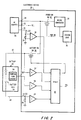
- FIG.2 shows an embodiment of an electronic device system according to the present invention.
- an AC adapter 20 as a power supply apparatus is detachably connected, through two power lines 22 and 28 and a control signal line 62, to an electronic apparatus 30.
- the electronic device 30 is, for example, a battery operable personal computer. However, the present invention may be applied to is not limited to a battery operable personal computer.
- a battery 40 is detachably connected to the electronic device 30 through two power lines 42 and 44 and a detection signal line 56.
- One power line 22 of the AC adapter 20 is grounded through a current detecting resistance 24.
- the electric potentials of both ends of the current detecting resistance 24 are input to a differential amplifier26 for detecting current, and a voltage signal corresponding to the output current value I(O) of the AC adapter 20 is output from the differential amplifier 26.
- the other power line 28 is connected, through a power-on switch 32, to a DC voltage converter 34, the output line of which is connected to a system load 36.
- the power-on switch 32 is turned on or off according to a control signal indicated by "PWR ON" in the figure.
- the control signal is generated by operating a system-on switch (not shown) of the electronic device 30.
- the power line 28 is also connected, through a battery-on switch 38, to one power line 42 of the battery 40.
- the other power line 44 of the battery 40 is grounded through a current detecting resistance 46.
- the electric potentials of both ends of the current detecting resistance 46 are input to a differential amplifier 48 for detecting current, and a voltage signal corresponding to the output current value Ibt(O) of the battery 40 is output from the differential amplifier 48.
- a voltage detecting amplifier 52 is connected to the power line 42 , from which a voltage signal indicating the terminal voltage of the battery 40 is output.
- a temperature sensor 54 as well as a battery cell 50.
- the output signal of the temperature sensor 54 is input, through the temperature detection signal line 56 of the battery 40, to a temperature detecting amplifier 58.
- the output signals of the battery current detecting amplifier 48, the battery voltage detecting amplifier 52, and the battery temperature detecting amplifier 58 are provided to a power management processor 60.
- the power management processor 60 is, for example, a one-chip computer provided with an analog-to-digital converter.
- the output signal of the AC power output current detecting amplifier 26 are also provided to the power management processor 60.
- the power management processor 60 outputs a control signal for turning on or off the battery-on switch 38.
- the power management processor 60 outputs a control mode switching signal indicated by "SEL" in the figure, and the signal is provided to the AC adapter 20 through the control signal line 62 of the AC adapter 20.
- the power management processor 60 obtains information about battery temperature from the output signal of the battery temperature detecting amplifier 58 and prevents a charging current from flowing into the battery 40 by turning off the battery-on switch 38 if it is determined that the battery temperature risen by a charge became higherthan a predetermined value. Further, the power management processor60 obtains information about battery voltage from the output signal of the battery voltage detecting amplifier 52 and prevents a charging current from flowing into the battery 40 by turning off the battery-on switch 38 if it is determined that the battery voltage was outside a predetermined range. Still further, the power management processor 60 obtains information about battery current from the output signal of the battery current detecting amplifier 48 and calculates the remaining capacity of a battery based on the information.
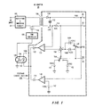
- FIG.1 shows the internal construction of the AC adapter20.
- a rectifying and smoothing circuit 102 rectifies and smoothes AC input.
- an AC generating switch 104 and the primary coil of a transformer 106 are connected in series.
- a value of voltage applied to the primary coil of the transformer 106 is controlled according to the on/off time of the switch 104.
- the on/off time of the switch 104 is controlled by a pulse width modulator (PWM) 108.
- PWM pulse width modulator
- an electric potential of the power line 28 is a power electric potential or an output electric potential V(O).
- the output electric potential V(O) is a voltage feedback value (voltage feedback signal).
- a current detection resistance 114 is provided, in series, to the power line 22.
- a resistance value of the resistance 114 is R(S) and a value of the current which flows through the resistance 114, that is, the output current of the AC adapter 20 is I(O).
- the output current I(O) is converted to a voltage signal [I(O) R(S)] by the current detection resistance 114 and [I(O) R(S)] becomes a current feedback signal.
- One of electric potentials of both ends of the current detection resistance 114 is input to a non-inverting input terminal of a first differential amplifier 120 and the other is input to an adder-subtracter 150.
- Added to the output electric potential V(O) is either a constant voltage V(Z1) generated by a first Zener diode 148Aora a constant voltage V(Z2) generated by a second Zenerdiode 148B. Avalue after addition is added to said other electric potential of the resistance 114 in the adder-subtracter 150. Further, in the adder-subtracter 150, either a reference voltage V(R1) generated by a first reference voltage generating circuit 151 or a reference voltage V(R2) generated by a second reference voltage generating circuit 152 is subtracted. The output of the adder-subtracter 150 is input to an inverting input terminal of the first differential amplifier 120.
- Whether a constant voltage V(Z1) generated by the Zener diode 148A is input to the adder-subtracter 150 or a constant voltage -V(Z2) generated by the Zener diode 148B is input to the adder-subtracter 150 is determined by operating a switch 146. Further, whether a reference voltage V(R1) generated by the reference voltage generating circuit 151 is inputted to the adder-subtracter 150 or a reference voltage V(R2) generated by the reference voltage generating circuit 152 is inputted to the adder-subtracter 150 is determined by operating a switch 154.
- the power management processor60 (FIG.2) outputs the signal "SEL" for operating the switches 146 and 154.
- the output signal of the differential amplifier 120 is input, through a counterflow checking diode 122, to one terminal of a light-emitting element 132 of a photocoupler 130.
- the other terminal of the light-emitting element 132 is connected to a power voltage V(O).
- One terminal of a photo sensitive element 134 of the photocoupler 130 is grounded, and the other terminal is connected to the PWM controller 108.
- the current detection resistance 114, the Zener diodes 148Aand 148B, the adder-subtracter 150, the first differential amplifier 120, the photocoupler 130, the PWM controller 108, the switch 104, the transformer 106, the diode 110, and the capacitor 112 comprise constant power feedback control means.
- the output electric potential V(O) is lower than a constant voltage V(Z1) generated by the Zener diode 148A or a constant voltage V(Z2) generated by the Zener diode 148B, current does not flow through the Zener diode 148A or 148B. Therefore, the input to the adder-subtracter 150 is not a voltage feedback signal V(O), but only a current feedback signal [I(O) R(S)], and the output of the AC adapter 20 becomes a constant current output. That is, in such a case, said constant powerfeedback control means functions as constant current feedback control means.
- the power line 28 is connected to an inverting input terminal of a second differential amplifier 140.
- a reference voltage generating circuit 142 for generating a reference voltage V(R3), the electric potential V(O) of the power line 28 is compared with a reference electric potential V(R3).
- the output of the second differential amplifier 140 is connected, through a counterflow checking diode 144, to the output of the counterflow checking diode 122 and then connected to the photocoupler 130.
- the second differential amplifier 140, the photocoupler 130, the PWM controller 108, the switch 104, the transformer 106, the diode 110, and the capacitor 112 compose constant voltage feedback control means. In the state where the constant voltage feedback control means operates, the output of the AC adapter 20 becomes a constant voltage output.
- the outputs of the first and second differential amplifiers 120 and 140 are connected to each other and then input to the photocoupler 130. If the load impedance of the AC adapter 20 is high, that is, if the output current value I(O) is smaller than a predetermined value, the output (sink current) of the first differential amplifier 120 substantially vanishes, said constant power feedback means through the first differential amplifier 120 does not function, the voltage feedback control means through the second differential amplifier 140 functions, and the output of the AC adapter 20 becomes a constant voltage output.
- the output (sink current) of the first differential amplifier 120 begins to increase and current feedback starts to work.
- the output voltage V(O) begins to lower
- the output (sink current) of the second differential amplifier 140 substantially vanishes, and both current feedback and voltage feedback by the first differential amplifier 120 come into operation. Consequently, the output of the AC adapter 20 becomes a nearly constant power output.
- the output of the AC adapter 20 becomes a nearly constant power state when the battery-on switch 38 (FIG.2) is turned on. Then, the power line 42 of the battery 40 is connected to the output line 28 of the AC adapter 20, the battery 40 is charged, and the output voltage of the AC adapter 20 depends upon the voltage of the power line 42 of the battery 40.
- a voltage feedback value of a feedback path through the Zener diode 148A or the Zener diode 148B becomes zero. Therefore, a feedback path through the first differential amplifier 120 works as a current feedback control means. That is, current feed back means formed by the current detection resistance 114, the first differential amplifier 120, the photocoupler 130, and the PWM controller 108 works and the output of the AC adapter 20 is controlled so as to become a constant current.
- Constant current control so performed that it obtains a desired current value depends on whether the reference voltage V(R1) of the first reference voltage generating circuit 151 was selected or the reference voltage V(R2) of the second reference voltage generating circuit 152 was selected.
- the selection of the reference voltage V(R1) and the reference voltage V(R2) depends on the "SEL" signal generated by the power management processor 60 (FIG.2).
- a voltage feedback value of a feedback path through the Zener diode 148A or the Zener diode 148B does not become zero, and both the voltage feedback value and a current feedback value from the current detection resistance 114 are added by the adder-subtracter 150. Therefore, a feedback path through the first differential amplifier 120 works as nearly constant power control feedback means, and the output of the AC adapter 20 is controlled so as to become a nearly constant power, based on both the current feedback value and the voltage feedback value.
- the power management processor60 When detecting that the power-on switch 32 is turned on and the system load 36 is in a usual operating condition (a condition that is not a power-saving mode), the power management processor60 makes the "SEL" signal active and turns the change-over switch 154 to the first reference voltage generating circuit 151 while it turns the change-over switch 146 to the first Zener diode 148A.
- the power management processor 60 When detecting that the power-on switch 32 is turned off or the system load 36 is working in a power-saving mode though the power-on switch 32 is turned on, the power management processor 60 makes the "SEL" signal inactive and turns the change-over switch 154 to the second reference voltage generating circuit 152 while it turns the control mode change-over switch 146 to the second Zener diode 148B.
- the following expression is established with respect to a feedback path which returns to the first differential amplifier 120 through the photocoupler 130 and the PWM controller 108 from the first differential amplifier 120:
- V(R2)/R(S) is a constant
- constant current control is performed in the AC adapter 20.
- V(R3) is a constant
- constant voltage control is performed in the AC adapter 20.
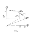
- FIG.3 shows the output characteristics of the AC adapter 20.
- the ordinate shows a value of an output voltage V(O) and the abscissa shows a value of an output current I(O).
- Region A is a region in which Equality 5 is established and constant voltage control is being performed. Then, the power-on switch 32 is turned on and the battery-on switch 38 is turned off.
- the AC adapter 20 provides constant voltage output to the system load 36.
- Region B is a region in which Equality 1 is established and nearly constant power control is being performed. Then, the control mode change-over switch 146 is turned to the first Zener diode 148A. Further, the power-on switch 32 is turned on and the battery-on switch 38 is turned on as well. The AC adapter 20 supplies an excess power as a charging current to the battery 40 while it supplies a drive current to the system load 36. Output in Region B makes it possible to charge the battery in a short time while a system is operating.
- Region C is a region in which Equality 2 is established and constant current control is being performed so that a current value may become a value determined by V(R1)/R(S). Then as well, the output of the AC adapter 20 supplies a charging current to the battery 40 while it supplies a drive current to the system load 36. Region C is provided to control a value of the charging current so that the changing current does not cause damage to the battery 40.
- Region D is a region in which Equality 4 is established and constant current control is being performed so that a current value may become a value determined by V(R2)/R(S). Then, the control mode change-over switch 146 is turned to the second Zener diode 148B. Further, the power-on switch 32 is turned off or the system load 36 is working in a power-saving mode even though the power-on switch 32 is turned on, and the battery-on switch 38 is turned on. The AC adapter 20 supplies a constant current determined by V(R2)/R(S) to the battery 40 and works as a quick charger.
- Region E is a region in which Equality 3 is established and nearly constant power control is performed. The region only restricts a maximum power which can be output by the AC adapter 20 and is not utilised for driving the system load 36 and for charging the battery 40.
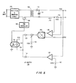
- FIG.4 shows an example of a specific circuit which comprises a feedback circuit section 400 of FIG. 1.
- AMP1 of FIG.4 corresponds to the differential amplifier 120 of FIG.1
- AMP2 of FIG.4 corresponds to the differential amplifier 140 of FIG.1.
- Resistances R3, R4, R5, R6, and R7 of FIG.4 compose the adder-subtracter 150 of FIG.1.
- a transistor Q1 of FIG.4 corresponds to the switch 154 of FIG.1.
- Vref generated by the resistance R3 and a reference voltage generating circuit ZD3 of FIG.4 corresponds to voltage generated by the reference voltage generating circuit 151 of FIG.1, and Vref generated by the resistance R5 and the reference voltage generating circuit ZD3 of FIG.4 corresponds to voltage generated by the reference voltage generating circuit 152 of FIG.1.
- ZD1 and ZD2 of FIG.4 correspond to the Zener diodes 148A and 148B of FIG.1, respectively.
- Transistors Q2 and Q3 of FIG.4 compose the switch 146 of FIG.1. Further,the object of the reference voltage generating circuit 142 on the side of the differential amplifier 140 of FIG.1 is attained by reference voltage Vref generated by the reference voltage generating circuit ZD3 of FIG.4.
- Resistances R8 and R9 of FIG.4 form the voltage feedback path from V(O).
- An AC adapter 200 of FIG.5 includes a multiplier 250, which multiplies the output of the first differential amplifier 120 by the voltage feedback quantity from V(O). Further, its output is subtracted from V(R4) by a subtracter. With respect to a feedback path which returns to the first differential amplifier 120 through the first differential amplifier 120, the multiplier 250, the photocoupler 130, and the PWM controller 108 the followina is established.
- C is the gain of the differential amplifier 120
- D is the gain of the entire feedback path including the photocoupler 130 and the PWM controller 108 and is infinite.
- FIG.6 shows the output characteristics of the AC adapter 200.
- the ordinate shows a value of an output voltage V(O) and the abscissa shows a value of an output current I(O).
- Region A is a region in which Equality 5 is established and constant voltage control is being performed, which is the same as in the AC adapter 20 of FIG.1.
- Region F is a region in which Equality 6 is established and constant power control is being performed. Then, the AC adapter 200 comes to supply an excess power as a charging current to a battery while it supplies a drive current to a system load.
Landscapes
- Engineering & Computer Science (AREA)
- Power Engineering (AREA)
- Business, Economics & Management (AREA)
- Emergency Management (AREA)
- Charge And Discharge Circuits For Batteries Or The Like (AREA)
Applications Claiming Priority (2)
| Application Number | Priority Date | Filing Date | Title |
|---|---|---|---|
| JP246338/92 | 1992-09-16 | ||
| JP4246338A JP2601974B2 (ja) | 1992-09-16 | 1992-09-16 | 電子機器用電源装置及び電子機器システム |
Publications (2)
| Publication Number | Publication Date |
|---|---|
| EP0588569A2 true EP0588569A2 (fr) | 1994-03-23 |
| EP0588569A3 EP0588569A3 (en) | 1994-05-25 |
Family
ID=17147082
Family Applications (1)
| Application Number | Title | Priority Date | Filing Date |
|---|---|---|---|
| EP19930307159 Withdrawn EP0588569A3 (en) | 1992-09-16 | 1993-09-10 | Power supply for electronic device, and electronic device system |
Country Status (3)
| Country | Link |
|---|---|
| US (1) | US5465039A (fr) |
| EP (1) | EP0588569A3 (fr) |
| JP (1) | JP2601974B2 (fr) |
Cited By (18)
| Publication number | Priority date | Publication date | Assignee | Title |
|---|---|---|---|---|
| EP0723326A2 (fr) * | 1995-01-19 | 1996-07-24 | Kyocera Corporation | Chargeur de batterie |
| EP0731549A2 (fr) * | 1995-03-08 | 1996-09-11 | International Business Machines Corporation | Chargeur de batterie |
| EP0696832A3 (fr) * | 1994-08-12 | 1997-05-28 | Ibm | Ensemble d'alimentation électrique d'un système électronique et méthode pour commander l'ensemble |
| EP0827253A1 (fr) * | 1996-05-22 | 1998-03-04 | Tai Her Yang | Circuit d'alimentation DC ayant un régulateur intermittant on/off |
| EP0852424A2 (fr) * | 1997-01-07 | 1998-07-08 | NOKIA TECHNOLOGY GmbH | Alimentation de puissance à découpage avec régulation cÔte primaire |
| EP1126591A2 (fr) * | 2000-01-22 | 2001-08-22 | M.K. Juchheim GmbH & Co. | Procédé et dispositif pour commander ou règler la puissance de résistances de chauffage à basse résistance |
| WO2001073918A2 (fr) * | 2000-03-30 | 2001-10-04 | Adc Telecommunications Israel Ltd. | Circuit d'alimentation à double limitation de tension |
| GB2382238A (en) * | 2001-08-25 | 2003-05-21 | Mackwell Electronics Ltd | Emergency lighting battery charging circuit |
| WO2006093669A2 (fr) * | 2005-02-25 | 2006-09-08 | Intel Corporation | Modification de la sortie d'un adaptateur de courant |
| EP1732199A2 (fr) * | 2005-06-10 | 2006-12-13 | Power Integrations, Inc. | Procédé et dispositif pour réduire la puissance maximale d'une source de puissance avec régulation de la région de transition |
| EP1531534A3 (fr) * | 2003-11-12 | 2007-09-05 | Nec Corporation | Procédé de commande et et dispositif pour charger et alimenter |
| US7673515B2 (en) | 2004-07-26 | 2010-03-09 | Spider Technologies Secutiry Ltd. | Vibration sensor |
| US8023290B2 (en) | 1997-01-24 | 2011-09-20 | Synqor, Inc. | High efficiency power converter |
| WO2012123140A3 (fr) * | 2011-03-11 | 2012-11-08 | Robert Bosch Gmbh | Partie de réseau de commutation pour un appareil de charge |
| EP2378623A3 (fr) * | 2010-04-19 | 2014-07-16 | Sony Mobile Communications Japan, Inc. | Appareil électronique portable et appareil de chargement |
| US9397560B2 (en) | 2014-08-15 | 2016-07-19 | Power Integrations, Inc. | Controller for a power supply with transition region regulation |
| US10199950B1 (en) | 2013-07-02 | 2019-02-05 | Vlt, Inc. | Power distribution architecture with series-connected bus converter |
| WO2019096715A1 (fr) * | 2017-11-15 | 2019-05-23 | Signify Holding B.V. | Convertisseur de puissance à découpage et procédé de conversion |
Families Citing this family (48)
| Publication number | Priority date | Publication date | Assignee | Title |
|---|---|---|---|---|
| CH687656A5 (de) * | 1993-10-12 | 1997-01-15 | Fischer Helmut | Stromversorgung fuer Bereitschaftsschaltungen von elektrischen Geraeten. |
| KR960027134A (ko) * | 1994-12-22 | 1996-07-22 | 김광호 | 만충전 배터리의 재충전 방지 기능을 갖는 충전장치 및 그 제어방법 |
| JP3540848B2 (ja) * | 1994-12-26 | 2004-07-07 | 富士通株式会社 | 充電制御装置及び電子機器 |
| JP3309266B2 (ja) * | 1995-02-28 | 2002-07-29 | 京セラ株式会社 | 電池パックの充電端子短絡防止回路 |
| US5656923A (en) * | 1995-04-10 | 1997-08-12 | The Whitaker Corporation | A DC power supply controller |
| US5625275A (en) * | 1995-05-24 | 1997-04-29 | Ast Research, Inc. | Power supply which provides a variable charging current to a battery in a portable computer system |
| CN1077341C (zh) * | 1995-08-10 | 2002-01-02 | 索尼公司 | 充电方法和充电装置 |
| US5698964A (en) * | 1995-10-20 | 1997-12-16 | Dell Usa, L.P. | Adaptive power battery charging apparatus |
| JP3737559B2 (ja) * | 1996-03-21 | 2006-01-18 | 株式会社沖データ | プリンタ装置及びその電源回路 |
| KR100222074B1 (ko) * | 1996-12-17 | 1999-10-01 | 윤종용 | 정전력충전회로 및 이를 이용한 휴대용 컴퓨터 |
| JP3735999B2 (ja) * | 1997-02-20 | 2006-01-18 | ソニー株式会社 | 充電装置 |
| JPH10257685A (ja) * | 1997-03-10 | 1998-09-25 | Oki Electric Ind Co Ltd | 2次電池の満充電の検出方法 |
| KR100259263B1 (ko) * | 1997-05-21 | 2000-06-15 | 윤종용 | 휴대용 컴퓨터 시스템의 배터리 충전회로 및 그 충전방법 |
| US5821730A (en) * | 1997-08-18 | 1998-10-13 | International Components Corp. | Low cost battery sensing technique |
| KR100539216B1 (ko) * | 1997-11-29 | 2006-02-28 | 페어차일드코리아반도체 주식회사 | 축전지 충전회로 |
| KR19990069292A (ko) * | 1998-02-06 | 1999-09-06 | 구자홍 | 역률개선용 전력 절감회로 |
| US6144187A (en) * | 1998-11-12 | 2000-11-07 | Fairchild Semiconductor Corporation | Power measurement for adaptive battery charger |
| US6191552B1 (en) | 1999-01-25 | 2001-02-20 | Dell Usa, L.P. | External universal battery charging apparatus and method |
| US6246215B1 (en) | 1999-03-08 | 2001-06-12 | O2 Micro International Limited | Buffer battery power supply system |
| US6201372B1 (en) * | 1999-09-08 | 2001-03-13 | Denso Corporation, Ltd. | Reserve power option for a portable electronic device |
| US6577512B2 (en) * | 2001-05-25 | 2003-06-10 | Koninklijke Philips Electronics N.V. | Power supply for LEDs |
| US6950950B2 (en) * | 2001-12-28 | 2005-09-27 | Hewlett-Packard Development Company, L.P. | Technique for conveying overload conditions from an AC adapter to a load powered by the adapter |
| US6593726B1 (en) * | 2002-02-15 | 2003-07-15 | Micron Technology, Inc. | Voltage converter system and method having a stable output voltage |
| US6597153B1 (en) | 2002-06-03 | 2003-07-22 | O2Micro International Limited | Fast transient charging circuit |
| US6873322B2 (en) * | 2002-06-07 | 2005-03-29 | 02Micro International Limited | Adaptive LCD power supply circuit |
| US7227652B2 (en) * | 2002-10-17 | 2007-06-05 | Lexmark International, Inc. | Switching power supply, method of operation and device-and-power-supply assembly |
| US7203048B2 (en) * | 2002-10-24 | 2007-04-10 | 02Micro International Limited | DC to DC controller with inrush current protection |
| US6989981B2 (en) * | 2002-10-24 | 2006-01-24 | 02Micro International Limited | Battery over voltage and over protection circuit and adjustable adapter current limit circuit |
| JP2004187351A (ja) * | 2002-11-29 | 2004-07-02 | Nec Corp | 携帯電話機およびその充電方法 |
| US7525291B1 (en) * | 2003-01-21 | 2009-04-28 | Microsemi Corporation | Linearly regulated battery charger |
| US6888338B1 (en) | 2003-01-27 | 2005-05-03 | O2Micro International Limited | Portable computer and docking station having charging circuits with remote power sensing capabilities |
| CN1578052B (zh) * | 2003-07-09 | 2010-04-28 | 三美电机株式会社 | Ac适配器及其充电方法 |
| JP4115501B2 (ja) * | 2004-02-27 | 2008-07-09 | 新電元工業株式会社 | 充電器及びこの充電器を備えたdc−dcコンバータ、並びにそれらの制御回路 |
| US7755330B2 (en) * | 2004-03-31 | 2010-07-13 | Texas Instruments Incorporated | Methods and systems for controlling an AC adapter and battery charger in a closed loop configuration |
| US20100116059A1 (en) * | 2004-07-26 | 2010-05-13 | Spider Technologies Security Ltd. | Vibration sensor having a single virtual center of mass |
| JP2006235767A (ja) * | 2005-02-23 | 2006-09-07 | Nec Corp | リミッタ付電流制御回路 |
| JP4967526B2 (ja) | 2006-08-22 | 2012-07-04 | 富士通セミコンダクター株式会社 | 電源装置の制御回路、電源装置及びその制御方法 |
| US8018204B2 (en) * | 2007-03-26 | 2011-09-13 | The Gillette Company | Compact ultra fast battery charger |
| JP4380747B2 (ja) * | 2007-07-25 | 2009-12-09 | ソニー株式会社 | 充電装置 |
| JP4805223B2 (ja) * | 2007-07-27 | 2011-11-02 | レノボ・シンガポール・プライベート・リミテッド | 充電システムおよび充電方法 |
| US20110278938A1 (en) * | 2010-05-12 | 2011-11-17 | Magistor Technologies, L.L.C. | Ac battery employing magistor technology |
| TW201202728A (en) * | 2010-07-12 | 2012-01-16 | Hon Hai Prec Ind Co Ltd | Charge circuit |
| EP2423694B1 (fr) * | 2010-08-31 | 2015-07-01 | ST-Ericsson SA | Procédé pour l'auto-test d'une batterie entièrement déchargée, une telle batterie de condensateur à double couche et circuit correspondant |
| CN101944758A (zh) * | 2010-09-24 | 2011-01-12 | 鸿富锦精密工业(深圳)有限公司 | 具有动态分配充电电流功能的电池管理系统和方法 |
| CN103036212B (zh) * | 2011-09-30 | 2016-10-05 | 皆盈绿动能科技股份有限公司 | 电池输出短路保护电路 |
| US9660114B2 (en) | 2015-06-25 | 2017-05-23 | International Business Machines Corporation | Temperature stabilization of an on-chip temperature-sensitive element |
| WO2017133391A1 (fr) | 2016-02-05 | 2017-08-10 | 广东欧珀移动通信有限公司 | Système de charge, procédé de protection pendant la charge, et adaptateur d'alimentation |
| WO2018068243A1 (fr) * | 2016-10-12 | 2018-04-19 | 广东欧珀移动通信有限公司 | Terminal mobile |
Citations (2)
| Publication number | Priority date | Publication date | Assignee | Title |
|---|---|---|---|---|
| US4536696A (en) * | 1983-07-14 | 1985-08-20 | At&T Bell Laboratories | Buck-boost converter with dual-mode control for battery charging |
| EP0223293A1 (fr) * | 1985-11-11 | 1987-05-27 | Koninklijke Philips Electronics N.V. | Circuit d'alimentation en courant |
Family Cites Families (8)
| Publication number | Priority date | Publication date | Assignee | Title |
|---|---|---|---|---|
| US4404472A (en) * | 1981-12-28 | 1983-09-13 | General Electric Company | Maximum power control for a solar array connected to a load |
| JPS60105100A (ja) * | 1983-11-14 | 1985-06-10 | 住友電気工業株式会社 | ル−プ式車輌検出器 |
| JPS636882A (ja) * | 1986-06-26 | 1988-01-12 | ザ スタンダ−ド オイル カンパニ− | タンデム構成の光電池装置 |
| JPH0769750B2 (ja) * | 1989-09-08 | 1995-07-31 | 三菱電機株式会社 | 太陽電池電源系 |
| JP2736128B2 (ja) * | 1989-09-20 | 1998-04-02 | 株式会社東芝 | 無線通信装置 |
| CA2132419C (fr) * | 1992-03-18 | 1996-12-17 | Gerald L. Brainard | Systeme combine d'alimentation electrique et de charge d'accumulateur |
| US5325040A (en) * | 1992-09-21 | 1994-06-28 | Motorola, Inc. | Method and apparatus for charging a battery powered electronic device |
| US5355073A (en) * | 1992-09-30 | 1994-10-11 | Compaq Computer Corporation | Battery pack sensor for an AC adapter |
-
1992
- 1992-09-16 JP JP4246338A patent/JP2601974B2/ja not_active Expired - Lifetime
-
1993
- 1993-09-09 US US08/118,899 patent/US5465039A/en not_active Expired - Fee Related
- 1993-09-10 EP EP19930307159 patent/EP0588569A3/en not_active Withdrawn
Patent Citations (2)
| Publication number | Priority date | Publication date | Assignee | Title |
|---|---|---|---|---|
| US4536696A (en) * | 1983-07-14 | 1985-08-20 | At&T Bell Laboratories | Buck-boost converter with dual-mode control for battery charging |
| EP0223293A1 (fr) * | 1985-11-11 | 1987-05-27 | Koninklijke Philips Electronics N.V. | Circuit d'alimentation en courant |
Non-Patent Citations (1)
| Title |
|---|
| IBM TECHNICAL DISCLOSURE BULLETIN vol. 332964, no. 7 , December 1992 , NEW-YORK pages 95 - 96 'charge system with cvcw+cc ac/dc adapter' * |
Cited By (40)
| Publication number | Priority date | Publication date | Assignee | Title |
|---|---|---|---|---|
| EP0696832A3 (fr) * | 1994-08-12 | 1997-05-28 | Ibm | Ensemble d'alimentation électrique d'un système électronique et méthode pour commander l'ensemble |
| US5811895A (en) * | 1994-08-12 | 1998-09-22 | International Business Machines Corp. | Power supply circuit for use with a battery and an AC power adaptor |
| EP0723326A2 (fr) * | 1995-01-19 | 1996-07-24 | Kyocera Corporation | Chargeur de batterie |
| EP0723326A3 (fr) * | 1995-01-19 | 1997-03-05 | Kyocera Corp | Chargeur de batterie |
| EP0731549A2 (fr) * | 1995-03-08 | 1996-09-11 | International Business Machines Corporation | Chargeur de batterie |
| EP0731549A3 (fr) * | 1995-03-08 | 1997-11-26 | International Business Machines Corporation | Chargeur de batterie |
| EP0827253A1 (fr) * | 1996-05-22 | 1998-03-04 | Tai Her Yang | Circuit d'alimentation DC ayant un régulateur intermittant on/off |
| EP0852424A2 (fr) * | 1997-01-07 | 1998-07-08 | NOKIA TECHNOLOGY GmbH | Alimentation de puissance à découpage avec régulation cÔte primaire |
| EP0852424A3 (fr) * | 1997-01-07 | 1999-03-03 | NOKIA TECHNOLOGY GmbH | Alimentation de puissance à découpage avec régulation cÔte primaire |
| US5978235A (en) * | 1997-01-07 | 1999-11-02 | Nokia Technology Gmbh | Primary adjusted switched-mode power supply |
| US9143042B2 (en) | 1997-01-24 | 2015-09-22 | Synqor, Inc. | High efficiency power converter |
| US8023290B2 (en) | 1997-01-24 | 2011-09-20 | Synqor, Inc. | High efficiency power converter |
| US8493751B2 (en) | 1997-01-24 | 2013-07-23 | Synqor, Inc. | High efficiency power converter |
| EP1126591A2 (fr) * | 2000-01-22 | 2001-08-22 | M.K. Juchheim GmbH & Co. | Procédé et dispositif pour commander ou règler la puissance de résistances de chauffage à basse résistance |
| EP1126591B1 (fr) * | 2000-01-22 | 2005-12-07 | JUMO GmbH & Co. KG | Procédé et dispositif pour commander ou règler la puissance de résistances de chauffage à basse résistance |
| WO2001073918A3 (fr) * | 2000-03-30 | 2002-03-14 | Adc Teledata Comm Ltd | Circuit d'alimentation à double limitation de tension |
| WO2001073918A2 (fr) * | 2000-03-30 | 2001-10-04 | Adc Telecommunications Israel Ltd. | Circuit d'alimentation à double limitation de tension |
| GB2382238B (en) * | 2001-08-25 | 2005-04-06 | Mackwell Electronics Ltd | Emergency lighting |
| GB2382238A (en) * | 2001-08-25 | 2003-05-21 | Mackwell Electronics Ltd | Emergency lighting battery charging circuit |
| EP1531534A3 (fr) * | 2003-11-12 | 2007-09-05 | Nec Corporation | Procédé de commande et et dispositif pour charger et alimenter |
| US7673515B2 (en) | 2004-07-26 | 2010-03-09 | Spider Technologies Secutiry Ltd. | Vibration sensor |
| CN101128791B (zh) * | 2005-02-25 | 2012-10-10 | 英特尔公司 | 改变电源适配器输出 |
| WO2006093669A3 (fr) * | 2005-02-25 | 2006-11-02 | Intel Corp | Modification de la sortie d'un adaptateur de courant |
| WO2006093669A2 (fr) * | 2005-02-25 | 2006-09-08 | Intel Corporation | Modification de la sortie d'un adaptateur de courant |
| US7853818B2 (en) | 2005-02-25 | 2010-12-14 | Intel Corporation | Modifying power adapter output |
| DE112006000296B4 (de) * | 2005-02-25 | 2012-03-29 | Intel Corp. | Modifizieren des Ausgangs eines Leistungsadapters |
| EP1732199A3 (fr) * | 2005-06-10 | 2009-01-21 | Power Integrations, Inc. | Procédé et dispositif pour réduire la puissance maximale d'une source de puissance avec régulation de la région de transition |
| US7728572B2 (en) | 2005-06-10 | 2010-06-01 | Power Integrations, Inc. | Method and apparatus to reduce maximum power from a power supply with transition region regulation |
| EP1732199A2 (fr) * | 2005-06-10 | 2006-12-13 | Power Integrations, Inc. | Procédé et dispositif pour réduire la puissance maximale d'une source de puissance avec régulation de la région de transition |
| US8188724B2 (en) | 2005-06-10 | 2012-05-29 | Power Integrations, Inc. | Method and apparatus to reduce maximum power from a power supply with transition region regulation |
| EP2378623A3 (fr) * | 2010-04-19 | 2014-07-16 | Sony Mobile Communications Japan, Inc. | Appareil électronique portable et appareil de chargement |
| US9166436B2 (en) | 2010-04-19 | 2015-10-20 | Sony Corporation | Portable electronic apparatus and charging apparatus |
| WO2012123140A3 (fr) * | 2011-03-11 | 2012-11-08 | Robert Bosch Gmbh | Partie de réseau de commutation pour un appareil de charge |
| US10594223B1 (en) | 2013-07-02 | 2020-03-17 | Vlt, Inc. | Power distribution architecture with series-connected bus converter |
| US11705820B2 (en) | 2013-07-02 | 2023-07-18 | Vicor Corporation | Power distribution architecture with series-connected bus converter |
| US10199950B1 (en) | 2013-07-02 | 2019-02-05 | Vlt, Inc. | Power distribution architecture with series-connected bus converter |
| US11075583B1 (en) | 2013-07-02 | 2021-07-27 | Vicor Corporation | Power distribution architecture with series-connected bus converter |
| US9397560B2 (en) | 2014-08-15 | 2016-07-19 | Power Integrations, Inc. | Controller for a power supply with transition region regulation |
| US9680384B2 (en) | 2014-08-15 | 2017-06-13 | Power Integrations, Inc. | Controller for a power supply with transition region regulation |
| WO2019096715A1 (fr) * | 2017-11-15 | 2019-05-23 | Signify Holding B.V. | Convertisseur de puissance à découpage et procédé de conversion |
Also Published As
| Publication number | Publication date |
|---|---|
| US5465039A (en) | 1995-11-07 |
| JPH06113477A (ja) | 1994-04-22 |
| EP0588569A3 (en) | 1994-05-25 |
| JP2601974B2 (ja) | 1997-04-23 |
Similar Documents
| Publication | Publication Date | Title |
|---|---|---|
| EP0588569A2 (fr) | Alimentation pour appareil électronique et système de dispositif électronique | |
| US11909317B2 (en) | Efficient use of energy in a switching power converter | |
| US6229286B1 (en) | Charging controller | |
| US5777462A (en) | Mode configurable DC power supply | |
| US7679343B2 (en) | Power supply system and method for controlling output voltage | |
| US4949028A (en) | Multiple voltage battery charge balancing and load protecting device | |
| US4581691A (en) | Balanced constant current sensing circuit inherently immune to longitudinal currents | |
| JP3395952B2 (ja) | 電気自動車用組み電池の電圧検出装置 | |
| US20060187689A1 (en) | Parallel powering of portable electrical devices | |
| US6617826B2 (en) | Charging device capable of dynamically adjusting charging power | |
| EP0899643A1 (fr) | Régulateur de tension linéaire à consommation réduite et à haute réjection d'alimentation | |
| KR100770959B1 (ko) | 전원 유닛 | |
| US20230216418A1 (en) | Systems and methods for voltage compensation based on load conditions in power converters | |
| KR20080076735A (ko) | 검출회로 및 전원 시스템 | |
| US4920307A (en) | Electric power source used to charge a secondary power source | |
| US5045768A (en) | Off-line battery charger | |
| US6232745B1 (en) | Charging controller | |
| US6275007B1 (en) | Charging controller | |
| US7701178B2 (en) | Charge control that keeps constant input voltage supplied to battery pack | |
| JPWO2014024244A1 (ja) | 電源回路、電子処理装置、および電力供給方法 | |
| US20050134235A1 (en) | Apparatus and method for constant delta current control in a capacitor charger | |
| KR100344876B1 (ko) | 충전회로 | |
| CN114744854B (zh) | 电源电路及电源芯片 | |
| JP3235135B2 (ja) | バッテリーチャージャー | |
| JPH0787682A (ja) | バッテリーチャージャー |
Legal Events
| Date | Code | Title | Description |
|---|---|---|---|
| PUAI | Public reference made under article 153(3) epc to a published international application that has entered the european phase |
Free format text: ORIGINAL CODE: 0009012 |
|
| AK | Designated contracting states |
Kind code of ref document: A2 Designated state(s): DE FR GB |
|
| PUAL | Search report despatched |
Free format text: ORIGINAL CODE: 0009013 |
|
| AK | Designated contracting states |
Kind code of ref document: A3 Designated state(s): DE FR GB |
|
| 17P | Request for examination filed |
Effective date: 19940718 |
|
| 17Q | First examination report despatched |
Effective date: 19951222 |
|
| STAA | Information on the status of an ep patent application or granted ep patent |
Free format text: STATUS: THE APPLICATION IS DEEMED TO BE WITHDRAWN |
|
| 18D | Application deemed to be withdrawn |
Effective date: 19970402 |