EP0583023A1 - Verfahren für DMOS-Transistor mit Grabenstruktur unter Verwendung von sechs Masken - Google Patents
Verfahren für DMOS-Transistor mit Grabenstruktur unter Verwendung von sechs Masken Download PDFInfo
- Publication number
- EP0583023A1 EP0583023A1 EP93202185A EP93202185A EP0583023A1 EP 0583023 A1 EP0583023 A1 EP 0583023A1 EP 93202185 A EP93202185 A EP 93202185A EP 93202185 A EP93202185 A EP 93202185A EP 0583023 A1 EP0583023 A1 EP 0583023A1
- Authority
- EP
- European Patent Office
- Prior art keywords
- layer
- forming
- principal surface
- transistor
- portions
- Prior art date
- Legal status (The legal status is an assumption and is not a legal conclusion. Google has not performed a legal analysis and makes no representation as to the accuracy of the status listed.)
- Granted
Links
- 238000004519 manufacturing process Methods 0.000 title description 11
- 238000000034 method Methods 0.000 claims abstract description 31
- 239000000758 substrate Substances 0.000 claims description 14
- 210000000746 body region Anatomy 0.000 claims description 13
- 229910052751 metal Inorganic materials 0.000 claims description 12
- 239000002184 metal Substances 0.000 claims description 12
- 238000005530 etching Methods 0.000 claims description 8
- 230000005669 field effect Effects 0.000 claims description 4
- 239000004065 semiconductor Substances 0.000 claims description 4
- 238000000151 deposition Methods 0.000 claims description 3
- 239000004020 conductor Substances 0.000 claims 4
- 238000009499 grossing Methods 0.000 claims 1
- 239000000463 material Substances 0.000 claims 1
- 230000001590 oxidative effect Effects 0.000 claims 1
- 230000000873 masking effect Effects 0.000 abstract description 22
- 229910021420 polycrystalline silicon Inorganic materials 0.000 description 24
- 229920005591 polysilicon Polymers 0.000 description 22
- 238000009792 diffusion process Methods 0.000 description 9
- XUIMIQQOPSSXEZ-UHFFFAOYSA-N Silicon Chemical compound [Si] XUIMIQQOPSSXEZ-UHFFFAOYSA-N 0.000 description 5
- 230000015572 biosynthetic process Effects 0.000 description 5
- 239000005380 borophosphosilicate glass Substances 0.000 description 5
- 229920002120 photoresistant polymer Polymers 0.000 description 5
- 230000003647 oxidation Effects 0.000 description 4
- 238000007254 oxidation reaction Methods 0.000 description 4
- 229910052710 silicon Inorganic materials 0.000 description 4
- 239000010703 silicon Substances 0.000 description 4
- ZOXJGFHDIHLPTG-UHFFFAOYSA-N Boron Chemical compound [B] ZOXJGFHDIHLPTG-UHFFFAOYSA-N 0.000 description 3
- 229910052796 boron Inorganic materials 0.000 description 3
- VYPSYNLAJGMNEJ-UHFFFAOYSA-N Silicium dioxide Chemical compound O=[Si]=O VYPSYNLAJGMNEJ-UHFFFAOYSA-N 0.000 description 2
- 229910052782 aluminium Inorganic materials 0.000 description 2
- XAGFODPZIPBFFR-UHFFFAOYSA-N aluminium Chemical compound [Al] XAGFODPZIPBFFR-UHFFFAOYSA-N 0.000 description 2
- 230000015556 catabolic process Effects 0.000 description 2
- 238000005516 engineering process Methods 0.000 description 2
- 239000007943 implant Substances 0.000 description 2
- 150000002500 ions Chemical class 0.000 description 2
- 150000004767 nitrides Chemical class 0.000 description 2
- 238000002161 passivation Methods 0.000 description 2
- 229910052582 BN Inorganic materials 0.000 description 1
- PZNSFCLAULLKQX-UHFFFAOYSA-N Boron nitride Chemical compound N#B PZNSFCLAULLKQX-UHFFFAOYSA-N 0.000 description 1
- 229910052581 Si3N4 Inorganic materials 0.000 description 1
- 229910052785 arsenic Inorganic materials 0.000 description 1
- RQNWIZPPADIBDY-UHFFFAOYSA-N arsenic atom Chemical compound [As] RQNWIZPPADIBDY-UHFFFAOYSA-N 0.000 description 1
- 230000009286 beneficial effect Effects 0.000 description 1
- 230000008021 deposition Effects 0.000 description 1
- 238000001312 dry etching Methods 0.000 description 1
- 238000012986 modification Methods 0.000 description 1
- 230000004048 modification Effects 0.000 description 1
- 239000005360 phosphosilicate glass Substances 0.000 description 1
- 235000012239 silicon dioxide Nutrition 0.000 description 1
- 239000000377 silicon dioxide Substances 0.000 description 1
- HQVNEWCFYHHQES-UHFFFAOYSA-N silicon nitride Chemical compound N12[Si]34N5[Si]62N3[Si]51N64 HQVNEWCFYHHQES-UHFFFAOYSA-N 0.000 description 1
- 238000004544 sputter deposition Methods 0.000 description 1
- 239000000126 substance Substances 0.000 description 1
Images
Classifications
-
- H—ELECTRICITY
- H01—ELECTRIC ELEMENTS
- H01L—SEMICONDUCTOR DEVICES NOT COVERED BY CLASS H10
- H01L29/00—Semiconductor devices specially adapted for rectifying, amplifying, oscillating or switching and having potential barriers; Capacitors or resistors having potential barriers, e.g. a PN-junction depletion layer or carrier concentration layer; Details of semiconductor bodies or of electrodes thereof ; Multistep manufacturing processes therefor
- H01L29/66—Types of semiconductor device ; Multistep manufacturing processes therefor
- H01L29/68—Types of semiconductor device ; Multistep manufacturing processes therefor controllable by only the electric current supplied, or only the electric potential applied, to an electrode which does not carry the current to be rectified, amplified or switched
- H01L29/76—Unipolar devices, e.g. field effect transistors
- H01L29/772—Field effect transistors
- H01L29/78—Field effect transistors with field effect produced by an insulated gate
- H01L29/7801—DMOS transistors, i.e. MISFETs with a channel accommodating body or base region adjoining a drain drift region
- H01L29/7802—Vertical DMOS transistors, i.e. VDMOS transistors
- H01L29/7811—Vertical DMOS transistors, i.e. VDMOS transistors with an edge termination structure
-
- H—ELECTRICITY
- H01—ELECTRIC ELEMENTS
- H01L—SEMICONDUCTOR DEVICES NOT COVERED BY CLASS H10
- H01L29/00—Semiconductor devices specially adapted for rectifying, amplifying, oscillating or switching and having potential barriers; Capacitors or resistors having potential barriers, e.g. a PN-junction depletion layer or carrier concentration layer; Details of semiconductor bodies or of electrodes thereof ; Multistep manufacturing processes therefor
- H01L29/66—Types of semiconductor device ; Multistep manufacturing processes therefor
- H01L29/68—Types of semiconductor device ; Multistep manufacturing processes therefor controllable by only the electric current supplied, or only the electric potential applied, to an electrode which does not carry the current to be rectified, amplified or switched
- H01L29/76—Unipolar devices, e.g. field effect transistors
-
- H—ELECTRICITY
- H01—ELECTRIC ELEMENTS
- H01L—SEMICONDUCTOR DEVICES NOT COVERED BY CLASS H10
- H01L29/00—Semiconductor devices specially adapted for rectifying, amplifying, oscillating or switching and having potential barriers; Capacitors or resistors having potential barriers, e.g. a PN-junction depletion layer or carrier concentration layer; Details of semiconductor bodies or of electrodes thereof ; Multistep manufacturing processes therefor
- H01L29/02—Semiconductor bodies ; Multistep manufacturing processes therefor
- H01L29/06—Semiconductor bodies ; Multistep manufacturing processes therefor characterised by their shape; characterised by the shapes, relative sizes, or dispositions of the semiconductor regions ; characterised by the concentration or distribution of impurities within semiconductor regions
- H01L29/0603—Semiconductor bodies ; Multistep manufacturing processes therefor characterised by their shape; characterised by the shapes, relative sizes, or dispositions of the semiconductor regions ; characterised by the concentration or distribution of impurities within semiconductor regions characterised by particular constructional design considerations, e.g. for preventing surface leakage, for controlling electric field concentration or for internal isolations regions
- H01L29/0607—Semiconductor bodies ; Multistep manufacturing processes therefor characterised by their shape; characterised by the shapes, relative sizes, or dispositions of the semiconductor regions ; characterised by the concentration or distribution of impurities within semiconductor regions characterised by particular constructional design considerations, e.g. for preventing surface leakage, for controlling electric field concentration or for internal isolations regions for preventing surface leakage or controlling electric field concentration
- H01L29/0611—Semiconductor bodies ; Multistep manufacturing processes therefor characterised by their shape; characterised by the shapes, relative sizes, or dispositions of the semiconductor regions ; characterised by the concentration or distribution of impurities within semiconductor regions characterised by particular constructional design considerations, e.g. for preventing surface leakage, for controlling electric field concentration or for internal isolations regions for preventing surface leakage or controlling electric field concentration for increasing or controlling the breakdown voltage of reverse biased devices
- H01L29/0615—Semiconductor bodies ; Multistep manufacturing processes therefor characterised by their shape; characterised by the shapes, relative sizes, or dispositions of the semiconductor regions ; characterised by the concentration or distribution of impurities within semiconductor regions characterised by particular constructional design considerations, e.g. for preventing surface leakage, for controlling electric field concentration or for internal isolations regions for preventing surface leakage or controlling electric field concentration for increasing or controlling the breakdown voltage of reverse biased devices by the doping profile or the shape or the arrangement of the PN junction, or with supplementary regions, e.g. junction termination extension [JTE]
- H01L29/0619—Semiconductor bodies ; Multistep manufacturing processes therefor characterised by their shape; characterised by the shapes, relative sizes, or dispositions of the semiconductor regions ; characterised by the concentration or distribution of impurities within semiconductor regions characterised by particular constructional design considerations, e.g. for preventing surface leakage, for controlling electric field concentration or for internal isolations regions for preventing surface leakage or controlling electric field concentration for increasing or controlling the breakdown voltage of reverse biased devices by the doping profile or the shape or the arrangement of the PN junction, or with supplementary regions, e.g. junction termination extension [JTE] with a supplementary region doped oppositely to or in rectifying contact with the semiconductor containing or contacting region, e.g. guard rings with PN or Schottky junction
-
- H—ELECTRICITY
- H01—ELECTRIC ELEMENTS
- H01L—SEMICONDUCTOR DEVICES NOT COVERED BY CLASS H10
- H01L29/00—Semiconductor devices specially adapted for rectifying, amplifying, oscillating or switching and having potential barriers; Capacitors or resistors having potential barriers, e.g. a PN-junction depletion layer or carrier concentration layer; Details of semiconductor bodies or of electrodes thereof ; Multistep manufacturing processes therefor
- H01L29/66—Types of semiconductor device ; Multistep manufacturing processes therefor
- H01L29/68—Types of semiconductor device ; Multistep manufacturing processes therefor controllable by only the electric current supplied, or only the electric potential applied, to an electrode which does not carry the current to be rectified, amplified or switched
- H01L29/76—Unipolar devices, e.g. field effect transistors
- H01L29/772—Field effect transistors
- H01L29/78—Field effect transistors with field effect produced by an insulated gate
- H01L29/7801—DMOS transistors, i.e. MISFETs with a channel accommodating body or base region adjoining a drain drift region
- H01L29/7802—Vertical DMOS transistors, i.e. VDMOS transistors
- H01L29/7813—Vertical DMOS transistors, i.e. VDMOS transistors with trench gate electrode, e.g. UMOS transistors
Definitions
- This invention relates to a method for fabricating a trenched DMOS transistor using six masking steps, resulting in a transistor having narrow trenches, shallow diffusions, and formed using relatively few process steps.
- DMOS transistors are well known as a type of MOSFET (metal on semiconductor field effect transistor) using diffusions to form the transistor regions, with a typical application being as a power transistor.
- MOSFET metal on semiconductor field effect transistor
- Such devices enjoy widespread use in such applications as automobile electrical systems, power supplies, and power management applications.
- Prior art trenched DMOS transistors have the shortcoming that typically it takes a fairly large number (such as eight or nine) fabrication masking steps to define the various transistor regions, including the tubs in which the active transistor regions are formed, the body region of the transistor, the source region of the transistor, the body contact regions, each of which are separate diffusions, and the termination structures, i.e. field plates and field rings. Additional masking steps are used to define the oxide layers and polysilicon portions of the transistor. Each additional masking step requires a mask alignment and thus results in the possibility of alignment error, undesirably reducing yield. Additionally, the many process steps which include temperature cycles tend to result in unwanted diffusion of certain of the implanted ions, thus undesirably altering the lateral extent and/or depth of various of the diffused regions.
- Polysilicon stringers are typically formed when a layer of polycrystalline silicon (“polysilicon”) is deposited over for instance an oxide layer which includes a step structure. Subsequent etching down of the polysilicon layer results in a portion of the polysilicon remaining adjacent to the step, since the polysilicon layer is thickest at that point. This "stringer" portion causes significant performance problems in the resulting transistor.
- a trenched DMOS transistor is formed having relatively narrow and relatively shallow trenches in one embodiment.
- the associated transistor active regions are relatively shallow diffusions. Only six masking steps are required because one mask is used to define both the deep body and the active areas of the transistor, i.e. establish the location of the tubs, and also to determine where local oxidation is to take place defining the field oxide portions of the transistor.
- both the prior art first mask which is typically used to define the tub region and the prior art second mask which is used to define the field oxidation regions are combined into one local oxidation of silicon (LOCOS) masking step.
- LOC local oxidation of silicon
- the fabrication process is simplified by eliminating any dedicated photoresist masking step for definition of both the body region and the source regions of the transistor. Instead, these regions are defined by the earlier active region mask which is patterned to define portions of the body regions and source regions and further by implanting and diffusing the body regions and source regions subsequent to gate trench formation, thus using the gate trench sidewalls partly to define the lateral extent of the source regions and body regions.
- Implanting of the body and source regions after formation of the trenches advantageously provides better control of the channel length of the completed transistors.
- Forming the body regions relatively late in the process advantageously exposes the body regions to fewer temperature cycles during fabrication and hence allows more accurate definition of the depth of the body diffusions.
- formation of the trench prior to formation of the body regions advantageously allows easier repair of etch damage to the trench sidewalls.
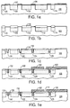
- Figures 1a through 1j show in cross section a sequence of steps to form a transistor in accordance with the present invention.
- the structure and method in accordance with the invention eliminate masking steps required in prior art processes, and may dispense with formation of a thick gate oxide, and yet still in one embodiment achieves breakdown voltage far in excess of that of the active cell transistor portion of the transistor. These characteristics are especially beneficial when high breakdown voltages are required and shallow junctions are required in accordance with high cell density.
- the active transistor cells are square or any other convenient geometry.
- an N-channel process in accordance with the invention uses an N- doped epitaxial layer 100 having a resistivity of for example 0.85 to 1 ohm-cm formed on an N+ doped silicon substrate having a resistivity of for example 0.001 to 0.005 ohm-cm and which is 5 to 10 microns (micrometers) thick (not shown).
- the substrate is about 500 ⁇ m thick.
- a thin layer of silicon dioxide 102 300 ⁇ to 500 ⁇ thick is thermally grown on the principal surface of the epitaxial layer 100 and a mask layer of silicon nitride 104 is deposited thereon.
- Mask layer 104 is conventionally patterned and etched.
- boron is predeposited by using the boron nitride process or by implanting boron at an energy of 40 to 60 KeV and a dose of 2 x 10¹³ to 1 x 10¹⁶/cm2 through the mask layer 104 and driven in to form P+ deep body regions 106, 108 which are about 2 to 3 microns deep and having a final concentration at the principal surface of 1 x 10¹⁶ to 2 x 10¹⁹/cm3, and similar P+ field rings (termination structures) 110, 112, 114.
- LOC local oxidation
- an LTO (low temperature oxide) second mask layer (not shown) is conventionally deposited and patterned, and trenches 120, 122, 124, 126 are each formed by anisotropic reactive ion dry etching to a depth of 1.5 to 3 microns and a width of 1 to 2 microns.
- Trenches 120, 122, 124 serve as the gate electrode trenches and trenches 124, 126 separate the field rings from adjacent structures.
- the gate oxide layer 130 is conventionally grown on the sidewalls of the trenches 120, 122, ..., 126 to a thickness of 400-800 ⁇ .
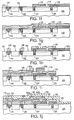
- the trenches are planarized by the deposition of a layer of polycrystalline silicon 132 which is at least as thick as the width of each trench.
- This relatively thick polysilicon layer 132 is partially dry etched away (without a mask) leaving a thickness of 0.5 microns.
- the substrate back side polysilicon and oxide layers are removed by wet chemical etch.
- the remaining polysilicon 132 is then doped to less than 2 ohm/square.
- masking of polysilicon 132 and a second polysilicon etching is performed, resulting in the structure of Figure 1d defining windows for subsequent processing.
- the use of the LOCOS oxide process eliminates the prior art "poly stringer" problem by reducing the oxide step height.
- a blanket N+ arsenic source implant and diffusion are performed at an energy of 60 to 120 KeV at a dosage of 1 x 10¹⁵ to 1 x 10¹⁶/cm2 to achieve a final surface concentration of 5 x 10¹⁹/cm3 in Figure 1f forming regions 140, 142.
- the N+ source junction 140, 142 depth is about 0.5 microns.
- BPSG boro-phosphosilicate glass
- Figure 1g a layer of boro-phosphosilicate glass (BPSG) 146 is conventionally deposited to a thickness of about 1.35 microns over the entire structure.
- BPSG layer 140 is masked and patterned to define the electrical contact openings 150, 152, 154, 156 to the transistor structure.
- the BPSG layer 140 is then conventionally reflowed to smooth the corners.
- a layer of metal 160 (e.g. aluminum or aluminum plus 1% silicon) is deposited such as by sputtering over the entire structure and etched using a conventional patterned metal mask layer.
- the polysilicon 132a at the edge termination is also etched away in this same step.
- the metal layer 160 is etched away in the termination region and this step also etches away unneeded portions 132a of the polysilicon layer in this region. Thus no separate masking layer is needed to remove unneeded polysilicon 132a in this step.
- a passivation layer 162 such as PSG or plasma nitride is conventionally deposited and by a mask step bonding pad holes (not shown) to contact the gate and source area are opened therethrough.
- the field rings 112, 114 are separated by insulated trench 126, thus allowing the field rings to be closely spaced together and hence conserving chip surface area. More field rings can be formed in a similar way.
- Trench 126 is filled with polysilicon that is electrically floating.
- Trench 124 is also filled with polysilicon and is electrically connected to the gate finger electrode connected in turn (outside the plane of Fig. 1i) to the polysilicon which is filling trenches 120, 122.
- the drain electrode is conventionally formed on the back side (not shown) of the substrate.
- the area immediately to the right of trench 122 has no active (source or body) regions and hence serves as a dummy cell adjacent to the termination structures; this dummy cell can be dispensed with in one embodiment. Also, the above described process can be implemented in a transistor having a termination other than that described herein.
Landscapes
- Microelectronics & Electronic Packaging (AREA)
- Engineering & Computer Science (AREA)
- Power Engineering (AREA)
- Condensed Matter Physics & Semiconductors (AREA)
- General Physics & Mathematics (AREA)
- Physics & Mathematics (AREA)
- Ceramic Engineering (AREA)
- Computer Hardware Design (AREA)
- Insulated Gate Type Field-Effect Transistor (AREA)
- Element Separation (AREA)
- Local Oxidation Of Silicon (AREA)
- Formation Of Insulating Films (AREA)
- Thin Film Transistor (AREA)
Applications Claiming Priority (2)
| Application Number | Priority Date | Filing Date | Title |
|---|---|---|---|
| US928909 | 1992-08-12 | ||
| US07/928,909 US5316959A (en) | 1992-08-12 | 1992-08-12 | Trenched DMOS transistor fabrication using six masks |
Publications (2)
| Publication Number | Publication Date |
|---|---|
| EP0583023A1 true EP0583023A1 (de) | 1994-02-16 |
| EP0583023B1 EP0583023B1 (de) | 1997-01-08 |
Family
ID=25456992
Family Applications (1)
| Application Number | Title | Priority Date | Filing Date |
|---|---|---|---|
| EP93202185A Expired - Lifetime EP0583023B1 (de) | 1992-08-12 | 1993-07-23 | Verfahren für DMOS-Transistor mit Grabenstruktur unter Verwendung von sechs Masken |
Country Status (5)
| Country | Link |
|---|---|
| US (1) | US5316959A (de) |
| EP (1) | EP0583023B1 (de) |
| JP (1) | JP3416214B2 (de) |
| KR (1) | KR100271721B1 (de) |
| DE (2) | DE583023T1 (de) |
Cited By (18)
| Publication number | Priority date | Publication date | Assignee | Title |
|---|---|---|---|---|
| NL9500370A (nl) * | 1994-02-24 | 1995-10-02 | Mitsubishi Electric Corp | Halfgeleiderinrichting en werkwijze voor het vervaardigen daarvan. |
| EP0675530A2 (de) * | 1994-03-31 | 1995-10-04 | Nippondenso Co., Ltd. | Herstellungsverfahren für ein Feldeffekt-Halbleiterbauelement |
| EP0726603A2 (de) * | 1995-02-10 | 1996-08-14 | SILICONIX Incorporated | Graben-Fieldeffekttransistor mit Sperrschicht-Barriere |
| EP0740352A2 (de) * | 1995-04-26 | 1996-10-30 | Nippondenso Co., Ltd. | MOS-gesteuerte Leistungsanordnung mit versenktem Gate und Verfahren zur Herstellung |
| EP0722189A3 (de) * | 1995-01-10 | 1997-02-05 | Siliconix Inc | Randabschlussmethode und Struktur für Leistungs-MOSFET |
| EP0797245A2 (de) * | 1996-03-22 | 1997-09-24 | Kabushiki Kaisha Toshiba | Verfahren zur Herstellung von einem vertikalen MOS-Halbleiterbauelement |
| US5776812A (en) * | 1994-03-30 | 1998-07-07 | Nippondenso Co., Ltd. | Manufacturing method of semiconductor device |
| US5780324A (en) * | 1994-03-30 | 1998-07-14 | Denso Corporation | Method of manufacturing a vertical semiconductor device |
| EP1009035A1 (de) * | 1997-08-29 | 2000-06-14 | Mitsubishi Denki Kabushiki Kaisha | Halbleiterbauelement mit isoliertem gatter und verfahren zu deren herstellung |
| WO2000042665A1 (de) * | 1999-01-11 | 2000-07-20 | Fraunhofer-Gesellschaft zur Förderung der angewandten Forschung e.V. | Mos-leistungsbauelement und verfahren zum herstellen desselben |
| EP1052690A2 (de) * | 1999-05-10 | 2000-11-15 | Intersil Corporation | Verfahren zur Herstellung von Bauelementen mit MOS-Gate und selbstjustierten Gräben |
| EP1160872A2 (de) | 1994-02-04 | 2001-12-05 | Mitsubishi Denki Kabushiki Kaisha | Halbleiterbauelement mit Graben |
| CN102117751B (zh) * | 2010-01-06 | 2012-12-12 | 上海华虹Nec电子有限公司 | 小线宽沟槽dmos的实现方法 |
| CN106298538A (zh) * | 2015-06-26 | 2017-01-04 | 北大方正集团有限公司 | Vdmos分压环的制造方法 |
| US9614043B2 (en) | 2012-02-09 | 2017-04-04 | Vishay-Siliconix | MOSFET termination trench |
| US9842911B2 (en) | 2012-05-30 | 2017-12-12 | Vishay-Siliconix | Adaptive charge balanced edge termination |
| US9882044B2 (en) | 2014-08-19 | 2018-01-30 | Vishay-Siliconix | Edge termination for super-junction MOSFETs |
| US9887259B2 (en) | 2014-06-23 | 2018-02-06 | Vishay-Siliconix | Modulated super junction power MOSFET devices |
Families Citing this family (58)
| Publication number | Priority date | Publication date | Assignee | Title |
|---|---|---|---|---|
| JPH0640559Y2 (ja) * | 1987-04-16 | 1994-10-26 | 日産自動車株式会社 | 船外機の支持装置 |
| JP2518868B2 (ja) * | 1987-10-13 | 1996-07-31 | 日産自動車株式会社 | 船外機の支持装置 |
| US5430324A (en) * | 1992-07-23 | 1995-07-04 | Siliconix, Incorporated | High voltage transistor having edge termination utilizing trench technology |
| US6110833A (en) * | 1998-03-03 | 2000-08-29 | Advanced Micro Devices, Inc. | Elimination of oxynitride (ONO) etch residue and polysilicon stringers through isolation of floating gates on adjacent bitlines by polysilicon oxidation |
| DE69525003T2 (de) * | 1994-08-15 | 2003-10-09 | Siliconix Inc., Santa Clara | Verfahren zum Herstellen eines DMOS-Transistors mit Grabenstruktur unter Verwendung von sieben Masken |
| US5592005A (en) * | 1995-03-31 | 1997-01-07 | Siliconix Incorporated | Punch-through field effect transistor |
| US5567634A (en) * | 1995-05-01 | 1996-10-22 | National Semiconductor Corporation | Method of fabricating self-aligned contact trench DMOS transistors |
| US5689128A (en) * | 1995-08-21 | 1997-11-18 | Siliconix Incorporated | High density trenched DMOS transistor |
| US5684319A (en) * | 1995-08-24 | 1997-11-04 | National Semiconductor Corporation | Self-aligned source and body contact structure for high performance DMOS transistors and method of fabricating same |
| KR0172262B1 (ko) * | 1995-12-30 | 1999-02-01 | 김주용 | 반도체 소자의 제조방법 |
| US5821583A (en) * | 1996-03-06 | 1998-10-13 | Siliconix Incorporated | Trenched DMOS transistor with lightly doped tub |
| US6090716A (en) * | 1996-12-17 | 2000-07-18 | Siliconix Incorporated | Method of fabricating a field effect transistor |
| US6103635A (en) * | 1997-10-28 | 2000-08-15 | Fairchild Semiconductor Corp. | Trench forming process and integrated circuit device including a trench |
| US6429481B1 (en) | 1997-11-14 | 2002-08-06 | Fairchild Semiconductor Corporation | Field effect transistor and method of its manufacture |
| US5939750A (en) | 1998-01-21 | 1999-08-17 | Advanced Micro Devices | Use of implanted ions to reduce oxide-nitride-oxide (ONO) etch residue and polystringers |
| US6043120A (en) * | 1998-03-03 | 2000-03-28 | Advanced Micro Devices, Inc. | Elimination of oxynitride (ONO) etch residue and polysilicon stringers through isolation of floating gates on adjacent bitlines by polysilicon oxidation |
| US6030868A (en) * | 1998-03-03 | 2000-02-29 | Advanced Micro Devices, Inc. | Elimination of oxynitride (ONO) etch residue and polysilicon stringers through isolation of floating gates on adjacent bitlines by polysilicon oxidation |
| US6051451A (en) * | 1998-04-21 | 2000-04-18 | Advanced Micro Devices, Inc. | Heavy ion implant process to eliminate polystringers in high density type flash memory devices |
| JP3514178B2 (ja) | 1998-09-16 | 2004-03-31 | 株式会社デンソー | 半導体装置の製造方法 |
| US5998833A (en) | 1998-10-26 | 1999-12-07 | North Carolina State University | Power semiconductor devices having improved high frequency switching and breakdown characteristics |
| US6621121B2 (en) * | 1998-10-26 | 2003-09-16 | Silicon Semiconductor Corporation | Vertical MOSFETs having trench-based gate electrodes within deeper trench-based source electrodes |
| US7229872B2 (en) * | 2000-04-04 | 2007-06-12 | International Rectifier Corporation | Low voltage power MOSFET device and process for its manufacture |
| TW523816B (en) * | 2000-06-16 | 2003-03-11 | Gen Semiconductor Inc | Semiconductor trench device with enhanced gate oxide integrity structure |
| JP4614522B2 (ja) * | 2000-10-25 | 2011-01-19 | 富士通セミコンダクター株式会社 | 半導体装置及びその製造方法 |
| GB0122121D0 (en) * | 2001-09-13 | 2001-10-31 | Koninkl Philips Electronics Nv | Edge termination in a trench-gate mosfet |
| JP3701227B2 (ja) * | 2001-10-30 | 2005-09-28 | 三菱電機株式会社 | 半導体装置及びその製造方法 |
| TW584935B (en) * | 2003-03-11 | 2004-04-21 | Mosel Vitelic Inc | Termination structure of DMOS device |
| US6992352B2 (en) | 2003-05-15 | 2006-01-31 | Analog Power Limited | Trenched DMOS devices and methods and processes for making same |
| JP4955958B2 (ja) * | 2005-08-04 | 2012-06-20 | ルネサスエレクトロニクス株式会社 | 半導体装置 |
| JP5050329B2 (ja) * | 2005-08-26 | 2012-10-17 | サンケン電気株式会社 | トレンチ構造半導体装置及びその製造方法 |
| DE102007063728B4 (de) * | 2006-03-07 | 2018-12-13 | Infineon Technologies Ag | Halbleiterbauelementanordnung mit einem Trench-Transistor |
| US8779506B2 (en) | 2006-03-07 | 2014-07-15 | Infineon Technologies Ag | Semiconductor component arrangement comprising a trench transistor |
| DE102007010884B4 (de) * | 2006-03-07 | 2010-10-07 | Infineon Technologies Ag | Verfahren zur Herstellung einer Halbleiterbauelementanordnung mit einem Trench-Transistor und Halbleiterbauelementanordnung mit einem Trench-Transistor |
| US8501561B2 (en) | 2006-03-07 | 2013-08-06 | Infineon Technologies Ag | Method for producing a semiconductor component arrangement comprising a trench transistor |
| US7816729B2 (en) * | 2006-08-08 | 2010-10-19 | Fwu-Iuan Hshieh | Trenched MOSFET device with trenched contacts |
| US20080206944A1 (en) * | 2007-02-23 | 2008-08-28 | Pan-Jit International Inc. | Method for fabricating trench DMOS transistors and schottky elements |
| US9484451B2 (en) * | 2007-10-05 | 2016-11-01 | Vishay-Siliconix | MOSFET active area and edge termination area charge balance |
| CN101604670B (zh) * | 2008-06-13 | 2012-12-05 | 北大方正集团有限公司 | 防止芯片压焊时金属层脱落的栅极焊点结构及其形成方法 |
| US8698232B2 (en) * | 2010-01-04 | 2014-04-15 | International Rectifier Corporation | Semiconductor device including a voltage controlled termination structure and method for fabricating same |
| TWI453831B (zh) | 2010-09-09 | 2014-09-21 | 台灣捷康綜合有限公司 | 半導體封裝結構及其製造方法 |
| US9431249B2 (en) | 2011-12-01 | 2016-08-30 | Vishay-Siliconix | Edge termination for super junction MOSFET devices |
| US8785997B2 (en) | 2012-05-16 | 2014-07-22 | Infineon Technologies Ag | Semiconductor device including a silicate glass structure and method of manufacturing a semiconductor device |
| US9966330B2 (en) | 2013-03-14 | 2018-05-08 | Vishay-Siliconix | Stack die package |
| US9589929B2 (en) | 2013-03-14 | 2017-03-07 | Vishay-Siliconix | Method for fabricating stack die package |
| DE102013108518B4 (de) * | 2013-08-07 | 2016-11-24 | Infineon Technologies Ag | Halbleitervorrichtung und verfahren zum herstellen derselben |
| US9508596B2 (en) | 2014-06-20 | 2016-11-29 | Vishay-Siliconix | Processes used in fabricating a metal-insulator-semiconductor field effect transistor |
| US10424646B2 (en) | 2017-09-26 | 2019-09-24 | Nxp Usa, Inc. | Field-effect transistor and method therefor |
| US10600911B2 (en) | 2017-09-26 | 2020-03-24 | Nxp Usa, Inc. | Field-effect transistor and method therefor |
| US10522677B2 (en) | 2017-09-26 | 2019-12-31 | Nxp Usa, Inc. | Field-effect transistor and method therefor |
| US10600879B2 (en) * | 2018-03-12 | 2020-03-24 | Nxp Usa, Inc. | Transistor trench structure with field plate structures |
| US10833174B2 (en) | 2018-10-26 | 2020-11-10 | Nxp Usa, Inc. | Transistor devices with extended drain regions located in trench sidewalls |
| US10749023B2 (en) | 2018-10-30 | 2020-08-18 | Nxp Usa, Inc. | Vertical transistor with extended drain region |
| US10749028B2 (en) | 2018-11-30 | 2020-08-18 | Nxp Usa, Inc. | Transistor with gate/field plate structure |
| DE102019122453A1 (de) | 2019-08-21 | 2021-02-25 | Infineon Technologies Austria Ag | Graben-Elektrodenstrukturen enthaltende Halbleitervorrichtung |
| US11387348B2 (en) | 2019-11-22 | 2022-07-12 | Nxp Usa, Inc. | Transistor formed with spacer |
| US11329156B2 (en) | 2019-12-16 | 2022-05-10 | Nxp Usa, Inc. | Transistor with extended drain region |
| US11217675B2 (en) | 2020-03-31 | 2022-01-04 | Nxp Usa, Inc. | Trench with different transverse cross-sectional widths |
| US11075110B1 (en) | 2020-03-31 | 2021-07-27 | Nxp Usa, Inc. | Transistor trench with field plate structure |
Citations (2)
| Publication number | Priority date | Publication date | Assignee | Title |
|---|---|---|---|---|
| DE3932621A1 (de) * | 1988-09-30 | 1990-04-05 | Toshiba Kawasaki Kk | Halbleitervorrichtung und verfahren zur herstellung derselben |
| FR2647596A1 (fr) * | 1989-05-24 | 1990-11-30 | Fuji Electric Co Ltd | Transistor a effet de champ a grille isolee et procede de fabrication |
Family Cites Families (4)
| Publication number | Priority date | Publication date | Assignee | Title |
|---|---|---|---|---|
| JPH01198076A (ja) * | 1988-02-02 | 1989-08-09 | Mitsubishi Electric Corp | 半導体装置 |
| JPH0783118B2 (ja) * | 1988-06-08 | 1995-09-06 | 三菱電機株式会社 | 半導体装置およびその製造方法 |
| US5019526A (en) * | 1988-09-26 | 1991-05-28 | Nippondenso Co., Ltd. | Method of manufacturing a semiconductor device having a plurality of elements |
| JPH0291976A (ja) * | 1988-09-29 | 1990-03-30 | Oki Electric Ind Co Ltd | 縦型溝型mos fetの製造方法 |
-
1992
- 1992-08-12 US US07/928,909 patent/US5316959A/en not_active Expired - Lifetime
-
1993
- 1993-07-23 DE DE0583023T patent/DE583023T1/de active Pending
- 1993-07-23 DE DE69307216T patent/DE69307216T2/de not_active Expired - Lifetime
- 1993-07-23 EP EP93202185A patent/EP0583023B1/de not_active Expired - Lifetime
- 1993-08-06 JP JP21515493A patent/JP3416214B2/ja not_active Expired - Lifetime
- 1993-08-09 KR KR1019930015387A patent/KR100271721B1/ko not_active IP Right Cessation
Patent Citations (2)
| Publication number | Priority date | Publication date | Assignee | Title |
|---|---|---|---|---|
| DE3932621A1 (de) * | 1988-09-30 | 1990-04-05 | Toshiba Kawasaki Kk | Halbleitervorrichtung und verfahren zur herstellung derselben |
| FR2647596A1 (fr) * | 1989-05-24 | 1990-11-30 | Fuji Electric Co Ltd | Transistor a effet de champ a grille isolee et procede de fabrication |
Non-Patent Citations (2)
| Title |
|---|
| INTERNATIONAL ELECTRON DEVICES MEETING 9 December 1990, SAN FRANCISCO, USA pages 793 - 797 K. SHENAI ET AL. * |
| PATENT ABSTRACTS OF JAPAN vol. 014, no. 288 (E-943)(4231) 21 June 1990 & JP-A-02 091 976 ( OKI ELECTRIC ) * |
Cited By (32)
| Publication number | Priority date | Publication date | Assignee | Title |
|---|---|---|---|---|
| EP1160872A3 (de) * | 1994-02-04 | 2007-06-20 | Mitsubishi Denki Kabushiki Kaisha | Halbleiterbauelement mit Graben |
| EP1160872A2 (de) | 1994-02-04 | 2001-12-05 | Mitsubishi Denki Kabushiki Kaisha | Halbleiterbauelement mit Graben |
| NL9500370A (nl) * | 1994-02-24 | 1995-10-02 | Mitsubishi Electric Corp | Halfgeleiderinrichting en werkwijze voor het vervaardigen daarvan. |
| US5780324A (en) * | 1994-03-30 | 1998-07-14 | Denso Corporation | Method of manufacturing a vertical semiconductor device |
| US5776812A (en) * | 1994-03-30 | 1998-07-07 | Nippondenso Co., Ltd. | Manufacturing method of semiconductor device |
| EP0675530A3 (de) * | 1994-03-31 | 1997-10-08 | Nippon Denso Co | Herstellungsverfahren für ein Feldeffekt-Halbleiterbauelement. |
| EP0675530A2 (de) * | 1994-03-31 | 1995-10-04 | Nippondenso Co., Ltd. | Herstellungsverfahren für ein Feldeffekt-Halbleiterbauelement |
| EP0722189A3 (de) * | 1995-01-10 | 1997-02-05 | Siliconix Inc | Randabschlussmethode und Struktur für Leistungs-MOSFET |
| US5614751A (en) * | 1995-01-10 | 1997-03-25 | Siliconix Incorporated | Edge termination structure for power MOSFET |
| EP0726603A2 (de) * | 1995-02-10 | 1996-08-14 | SILICONIX Incorporated | Graben-Fieldeffekttransistor mit Sperrschicht-Barriere |
| EP0726603A3 (de) * | 1995-02-10 | 1997-01-08 | Siliconix Inc | Graben-Fieldeffekttransistor mit Sperrschicht-Barriere |
| US5917216A (en) * | 1995-02-10 | 1999-06-29 | Siliconix Incorporated | Trenched field effect transistor with PN depletion barrier |
| EP0740352A2 (de) * | 1995-04-26 | 1996-10-30 | Nippondenso Co., Ltd. | MOS-gesteuerte Leistungsanordnung mit versenktem Gate und Verfahren zur Herstellung |
| EP0740352B1 (de) * | 1995-04-26 | 2003-01-15 | Denso Corporation | MOS-gesteuerte Leistungsanordnung mit versenktem Gate und Verfahren zur Herstellung |
| EP0797245A2 (de) * | 1996-03-22 | 1997-09-24 | Kabushiki Kaisha Toshiba | Verfahren zur Herstellung von einem vertikalen MOS-Halbleiterbauelement |
| EP0797245A3 (de) * | 1996-03-22 | 1998-05-13 | Kabushiki Kaisha Toshiba | Verfahren zur Herstellung von einem vertikalen MOS-Halbleiterbauelement |
| EP1009035A4 (de) * | 1997-08-29 | 2003-01-08 | Mitsubishi Electric Corp | Halbleiterbauelement mit isoliertem gatter und verfahren zu deren herstellung |
| EP1009035A1 (de) * | 1997-08-29 | 2000-06-14 | Mitsubishi Denki Kabushiki Kaisha | Halbleiterbauelement mit isoliertem gatter und verfahren zu deren herstellung |
| WO2000042665A1 (de) * | 1999-01-11 | 2000-07-20 | Fraunhofer-Gesellschaft zur Förderung der angewandten Forschung e.V. | Mos-leistungsbauelement und verfahren zum herstellen desselben |
| US6462376B1 (en) | 1999-01-11 | 2002-10-08 | Fraunhofer-Gesellschaft Zur Foerderung Der Angewandten Forschung E.V. | Power MOS element and method for producing the same |
| EP1052690A2 (de) * | 1999-05-10 | 2000-11-15 | Intersil Corporation | Verfahren zur Herstellung von Bauelementen mit MOS-Gate und selbstjustierten Gräben |
| EP1052690A3 (de) * | 1999-05-10 | 2003-12-03 | Intersil Corporation | Verfahren zur Herstellung von Bauelementen mit MOS-Gate und selbstjustierten Gräben |
| CN102117751B (zh) * | 2010-01-06 | 2012-12-12 | 上海华虹Nec电子有限公司 | 小线宽沟槽dmos的实现方法 |
| US9614043B2 (en) | 2012-02-09 | 2017-04-04 | Vishay-Siliconix | MOSFET termination trench |
| US9935193B2 (en) | 2012-02-09 | 2018-04-03 | Siliconix Technology C. V. | MOSFET termination trench |
| US10229988B2 (en) | 2012-05-30 | 2019-03-12 | Vishay-Siliconix | Adaptive charge balanced edge termination |
| US9842911B2 (en) | 2012-05-30 | 2017-12-12 | Vishay-Siliconix | Adaptive charge balanced edge termination |
| US10283587B2 (en) | 2014-06-23 | 2019-05-07 | Vishay-Siliconix | Modulated super junction power MOSFET devices |
| US9887259B2 (en) | 2014-06-23 | 2018-02-06 | Vishay-Siliconix | Modulated super junction power MOSFET devices |
| US9882044B2 (en) | 2014-08-19 | 2018-01-30 | Vishay-Siliconix | Edge termination for super-junction MOSFETs |
| US10340377B2 (en) | 2014-08-19 | 2019-07-02 | Vishay-Siliconix | Edge termination for super-junction MOSFETs |
| CN106298538A (zh) * | 2015-06-26 | 2017-01-04 | 北大方正集团有限公司 | Vdmos分压环的制造方法 |
Also Published As
| Publication number | Publication date |
|---|---|
| EP0583023B1 (de) | 1997-01-08 |
| KR940004839A (ko) | 1994-03-16 |
| DE583023T1 (de) | 1995-03-16 |
| US5316959A (en) | 1994-05-31 |
| DE69307216D1 (de) | 1997-02-20 |
| KR100271721B1 (ko) | 2000-11-15 |
| JPH06112497A (ja) | 1994-04-22 |
| JP3416214B2 (ja) | 2003-06-16 |
| DE69307216T2 (de) | 1997-05-22 |
Similar Documents
| Publication | Publication Date | Title |
|---|---|---|
| US5316959A (en) | Trenched DMOS transistor fabrication using six masks | |
| US5639676A (en) | Trenched DMOS transistor fabrication having thick termination region oxide | |
| US5689128A (en) | High density trenched DMOS transistor | |
| US5567634A (en) | Method of fabricating self-aligned contact trench DMOS transistors | |
| EP0777910B1 (de) | Verfahren zur herstellung eines mos gesteuerten bauelements mit reduzierter maskenzahl | |
| EP1393362B1 (de) | Verfahren zur Herstellung einer Halbleiteranordnung mit Graben-Gate | |
| KR100759939B1 (ko) | 트렌치 mosfet 디바이스 및 이러한 디바이스의 형성 방법 | |
| US6277695B1 (en) | Method of forming vertical planar DMOSFET with self-aligned contact | |
| EP1085577A2 (de) | Leistungs-Feldeffekttransistor mit einer Graben-Gateelektrode und Verfahren zu dessen Herstellung | |
| US20040145015A1 (en) | Field effect transistor and method of its manufacture | |
| US5663079A (en) | Method of making increased density MOS-gated semiconductor devices | |
| EP1386352B1 (de) | Halbleiteranordnungen mit graben-gateelektrode und verfahren zu deren herstellung | |
| US20020061623A1 (en) | Semiconductor trench device with enhanced gate oxide integrity structure | |
| US5668026A (en) | DMOS fabrication process implemented with reduced number of masks | |
| US6087224A (en) | Manufacture of trench-gate semiconductor devices | |
| US5702987A (en) | Method of manufacture of self-aligned JFET | |
| KR100272051B1 (ko) | 접점윈도우를통해베이스주입한p-채널mos게이트소자제조공정 | |
| US5904525A (en) | Fabrication of high-density trench DMOS using sidewall spacers | |
| EP0996970B1 (de) | Herstellung von feldeffekt-halbleiteranordnungen | |
| EP0225426A2 (de) | Verfahren zum Herstellen eines MOS-Transistors auf einem Substrat | |
| KR19980061673A (ko) | 트렌치 게이트형 절연게이트바이폴라 트랜지스터(전력트랜지스터)의 제조방법 | |
| KR19980014825A (ko) | 반도체 장치 제조방법 |
Legal Events
| Date | Code | Title | Description |
|---|---|---|---|
| PUAI | Public reference made under article 153(3) epc to a published international application that has entered the european phase |
Free format text: ORIGINAL CODE: 0009012 |
|
| AK | Designated contracting states |
Kind code of ref document: A1 Designated state(s): DE IT NL |
|
| 17P | Request for examination filed |
Effective date: 19940511 |
|
| ITCL | It: translation for ep claims filed |
Representative=s name: NOTARBARTOLO & GERVASI S.R.L. |
|
| TCNL | Nl: translation of patent claims filed | ||
| 17Q | First examination report despatched |
Effective date: 19940801 |
|
| DET | De: translation of patent claims | ||
| GRAG | Despatch of communication of intention to grant |
Free format text: ORIGINAL CODE: EPIDOS AGRA |
|
| GRAH | Despatch of communication of intention to grant a patent |
Free format text: ORIGINAL CODE: EPIDOS IGRA |
|
| GRAH | Despatch of communication of intention to grant a patent |
Free format text: ORIGINAL CODE: EPIDOS IGRA |
|
| ITF | It: translation for a ep patent filed | ||
| GRAA | (expected) grant |
Free format text: ORIGINAL CODE: 0009210 |
|
| AK | Designated contracting states |
Kind code of ref document: B1 Designated state(s): DE IT NL |
|
| REF | Corresponds to: |
Ref document number: 69307216 Country of ref document: DE Date of ref document: 19970220 |
|
| PLBE | No opposition filed within time limit |
Free format text: ORIGINAL CODE: 0009261 |
|
| STAA | Information on the status of an ep patent application or granted ep patent |
Free format text: STATUS: NO OPPOSITION FILED WITHIN TIME LIMIT |
|
| 26N | No opposition filed | ||
| PGFP | Annual fee paid to national office [announced via postgrant information from national office to epo] |
Ref country code: NL Payment date: 20030703 Year of fee payment: 11 |
|
| PG25 | Lapsed in a contracting state [announced via postgrant information from national office to epo] |
Ref country code: NL Free format text: LAPSE BECAUSE OF NON-PAYMENT OF DUE FEES Effective date: 20050201 |
|
| NLV4 | Nl: lapsed or anulled due to non-payment of the annual fee |
Effective date: 20050201 |
|
| PG25 | Lapsed in a contracting state [announced via postgrant information from national office to epo] |
Ref country code: IT Free format text: LAPSE BECAUSE OF NON-PAYMENT OF DUE FEES;WARNING: LAPSES OF ITALIAN PATENTS WITH EFFECTIVE DATE BEFORE 2007 MAY HAVE OCCURRED AT ANY TIME BEFORE 2007. THE CORRECT EFFECTIVE DATE MAY BE DIFFERENT FROM THE ONE RECORDED. Effective date: 20050723 |
|
| PGFP | Annual fee paid to national office [announced via postgrant information from national office to epo] |
Ref country code: DE Payment date: 20120727 Year of fee payment: 20 |
|
| REG | Reference to a national code |
Ref country code: DE Ref legal event code: R071 Ref document number: 69307216 Country of ref document: DE |
|
| PG25 | Lapsed in a contracting state [announced via postgrant information from national office to epo] |
Ref country code: DE Free format text: LAPSE BECAUSE OF EXPIRATION OF PROTECTION Effective date: 20130724 |