EP0580467B1 - Speichermatrix mit segmentierten Spalten - Google Patents
Speichermatrix mit segmentierten Spalten Download PDFInfo
- Publication number
- EP0580467B1 EP0580467B1 EP93401631A EP93401631A EP0580467B1 EP 0580467 B1 EP0580467 B1 EP 0580467B1 EP 93401631 A EP93401631 A EP 93401631A EP 93401631 A EP93401631 A EP 93401631A EP 0580467 B1 EP0580467 B1 EP 0580467B1
- Authority
- EP
- European Patent Office
- Prior art keywords
- segmented
- bit lines
- array
- pair
- column
- Prior art date
- Legal status (The legal status is an assumption and is not a legal conclusion. Google has not performed a legal analysis and makes no representation as to the accuracy of the status listed.)
- Expired - Lifetime
Links
- 230000015654 memory Effects 0.000 title claims description 31
- 238000003491 array Methods 0.000 claims description 33
- 230000007547 defect Effects 0.000 claims description 8
- 238000000638 solvent extraction Methods 0.000 claims description 4
- 238000000034 method Methods 0.000 claims 4
- 230000000295 complement effect Effects 0.000 claims 3
- 229910052751 metal Inorganic materials 0.000 description 76
- 239000002184 metal Substances 0.000 description 76
- 239000011295 pitch Substances 0.000 description 21
- 230000002829 reductive effect Effects 0.000 description 14
- 238000009792 diffusion process Methods 0.000 description 12
- 229910052782 aluminium Inorganic materials 0.000 description 7
- XAGFODPZIPBFFR-UHFFFAOYSA-N aluminium Chemical compound [Al] XAGFODPZIPBFFR-UHFFFAOYSA-N 0.000 description 7
- 230000011218 segmentation Effects 0.000 description 7
- 230000000694 effects Effects 0.000 description 3
- 239000007943 implant Substances 0.000 description 3
- ZOXJGFHDIHLPTG-UHFFFAOYSA-N Boron Chemical compound [B] ZOXJGFHDIHLPTG-UHFFFAOYSA-N 0.000 description 2
- 229910052796 boron Inorganic materials 0.000 description 2
- 239000002784 hot electron Substances 0.000 description 2
- 238000004519 manufacturing process Methods 0.000 description 2
- 230000035945 sensitivity Effects 0.000 description 2
- 239000000758 substrate Substances 0.000 description 2
- XUIMIQQOPSSXEZ-UHFFFAOYSA-N Silicon Chemical compound [Si] XUIMIQQOPSSXEZ-UHFFFAOYSA-N 0.000 description 1
- 230000001154 acute effect Effects 0.000 description 1
- 230000002411 adverse Effects 0.000 description 1
- 230000001186 cumulative effect Effects 0.000 description 1
- 230000002950 deficient Effects 0.000 description 1
- 230000001419 dependent effect Effects 0.000 description 1
- 238000007599 discharging Methods 0.000 description 1
- 238000005516 engineering process Methods 0.000 description 1
- 230000006870 function Effects 0.000 description 1
- 238000002347 injection Methods 0.000 description 1
- 239000007924 injection Substances 0.000 description 1
- 230000010354 integration Effects 0.000 description 1
- 238000002955 isolation Methods 0.000 description 1
- 238000001465 metallisation Methods 0.000 description 1
- 238000012856 packing Methods 0.000 description 1
- 238000005192 partition Methods 0.000 description 1
- 230000000717 retained effect Effects 0.000 description 1
- 230000002441 reversible effect Effects 0.000 description 1
- 239000004065 semiconductor Substances 0.000 description 1
- 238000000926 separation method Methods 0.000 description 1
- 229910052710 silicon Inorganic materials 0.000 description 1
- 239000010703 silicon Substances 0.000 description 1
- 239000007787 solid Substances 0.000 description 1
- 239000000243 solution Substances 0.000 description 1
- 230000003068 static effect Effects 0.000 description 1
Images


Classifications
-
- G—PHYSICS
- G11—INFORMATION STORAGE
- G11C—STATIC STORES
- G11C16/00—Erasable programmable read-only memories
- G11C16/02—Erasable programmable read-only memories electrically programmable
- G11C16/04—Erasable programmable read-only memories electrically programmable using variable threshold transistors, e.g. FAMOS
- G11C16/0491—Virtual ground arrays
-
- G—PHYSICS
- G11—INFORMATION STORAGE
- G11C—STATIC STORES
- G11C5/00—Details of stores covered by group G11C11/00
- G11C5/06—Arrangements for interconnecting storage elements electrically, e.g. by wiring
- G11C5/063—Voltage and signal distribution in integrated semi-conductor memory access lines, e.g. word-line, bit-line, cross-over resistance, propagation delay
-
- G—PHYSICS
- G11—INFORMATION STORAGE
- G11C—STATIC STORES
- G11C7/00—Arrangements for writing information into, or reading information out from, a digital store
- G11C7/18—Bit line organisation; Bit line lay-out
-
- H—ELECTRICITY
- H10—SEMICONDUCTOR DEVICES; ELECTRIC SOLID-STATE DEVICES NOT OTHERWISE PROVIDED FOR
- H10B—ELECTRONIC MEMORY DEVICES
- H10B69/00—Erasable-and-programmable ROM [EPROM] devices not provided for in groups H10B41/00 - H10B63/00, e.g. ultraviolet erasable-and-programmable ROM [UVEPROM] devices
Definitions
- Any memory cell in the array can be programmed or read by application of appropriate voltages to the word line and the bit lines connected to it.
- the state of an addressed memory cell can be determined by sensing the current flowing through its source and drain by means of the bit lines connected to them.
- the source and drain bit lines they can be implemented as buried diffusion bit lines.
- bit line series resistance is to parallel the buried diffusion bit lines with lower resistivity metal lines, as disclosed in EP-A-0 461 764.
- metal strips are overlaid on the bit lines but generally insulated from them by a dielectric layer in between.
- a series of metal contact (vias) at intervals along a buried diffusion bit line establish contacts with a corresponding metal strip.
- the intervals may be as short as 1 contact every 2 cells in high speed static RAM's, dynamic RAM's, ROM, EPROM, EEPROM or flash EEPROM.
- the authors arrange the sense amplifiers for adjacent bit lines alternately at the top and bottom of the segment. This allows each sense amplifier to occupy double the spacing of the columns.
- the architecture has the disadvantage of using multiple sense amplifiers; one set is used for every segment. The pitches of the metal lines and the select transistors remain the same as that of the bit lines.
- a segmented array is also employed to reduce bit line series resistance.
- the ROM is divided into 256 banks. Each bank is essentially a segmented column consisting of 16 word lines. Only one set of sense amplifiers is used for the whole array, and it is selectively switched onto even or odd columns by means of aluminum lines.
- the pair of segmented bit lines in each column are connectable to a pair of aluminum lines by bank-select transistors at all four ends, at the top and bottom of the segment.
- the aluminum lines run zigzag in the column direction between even and odd adjacent columns, and alternate in the middle of each segment.
- This architecture is such that the pitch of the aluminum lines is double that of the bit lines. This allows the aluminum lines to be further apart, thereby reducing the possibility of shorts.
- the disadvantage is that the pitch of the select transistors remains the same as that of the bit line and therefore limits the ultimate size and therefore the conductance of the select transistors.
- the bit line capacitance is not optimally reduced because the bank selection is such that when a column is selected, its source line and drain line are respectively shorted with the source line of the left adjacent column and the drain line of the right adjacent column. The selected bit lines are therefore coupled to the capacitance of other bit lines that are not selected.
- a two-dimensional array of memory cells arranged in rows and columns is partitioned into a plurality of segmented arrays along the column direction. In this way, the bit line connecting to all the sources or drains of transistors in a column is also segmented.
- Segmentation can significantly reduce bit-line resistance and capacitance, resulting in faster access time, among other things. It also isolates defects to the segments in which they are found, without the need to retire a much larger area if not the whole array.
- segment-select transistors are connected to every segmented bit lines alternately from the top and the bottom of a segmented array.
- Each segment-select transistor connects a segmented buried diffusion bit line to an overlying conductive strip or metal line via a metal contact in between two segmented arrays.
- Each metal line parallels a corresponding bit line but is otherwise insulated from it.
- Each metal contact point in between two segmented arrays is shared by the in-line bit lines from adjacent segment arrays connectable to it via segment-select transistors.
- This embodiment allows the segment-select transistors to be larger since they have twice the pitch of the bit lines. This makes segmentation of programmable memory arrays such as EPROM, EEPROM and Flash EEPROM possible. It also allows the metal contacts to be larger and fewer by one half since they also have twice the pitch of the bit lines, and allows them to be formed more easily since they are located outside the array regions between the two segment-select transistors which select either the segment immediately above or the segment immediately below the contact.
- the conductive strips or metal lines have double the pitch of the bit lines, such that each metal line is overlaid on two bit lines.
- a metal contact made with each metal line is located in line with but not connected to every four bit lines in between segmented arrays.
- Two segment-select transistors selectively connect each metal contact to the left or right bit line thereof.
- the left or right bit lines extend across adjacent segmented arrays immediately above and below the segment-select transistor. This configuration is repeated in between segments at alternate segments.
- Another similar set of metal contacts and segment-select transistors is located at the other alternate segments but offset by one bit line.
- the alternative embodiment allows the segment-select transistors to have even larger size since their pitch is four times that of the bit lines.
- the metal contacts have a pitch four times that of the bit lines. The number of contacts is reduced by three quarters. Also the double pitch of the metal line allows wider metal lines and consequently less problem with short or open circuits.
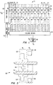
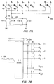
- Fig. 1 is a schematic illustration of an architecture of a conventional memory device.
- a two-dimensional array of memory cells 10 is formed by arranging transistors into rows and columns.
- a transistor 20 in the array typically comprises a source 22, a drain 24 and a control gate 26.
- Fig. 1 illustrates a memory array with a "virtual ground" architecture in which the transistors along each row are daisy-chained together by their sources and drains. Thus the drain of transistor 30 is connected to the source of transistor 20 on the right, and so on.
- An X-Y addressing system is effected by a set of word lines parallel to the rows and a set of bit lines parallel to the columns.
- a word line (such as 40, 42) connects the control gate (such as 26) of all transistors in one row.
- a bit line (such as 50, 52) connects to either the sources or drains of all transistors in one column.
- the bit lines (such as 50, 52) are paralleled by corresponding conductive strips or metal lines (such as 60, 62). Typically these are aluminum strips overlaid on the bit lines but generally insulated from them by a dielectric layer in between.
- a series of metal contacts (such as 70, 72) at intervals along a bit line establish contacts with a corresponding metal strip. For example, the contact 70 connects the bit line 50 to the metal line 60.
- a transistor or memory cell such as 80 When a transistor or memory cell such as 80 is addressed, appropriate voltages must be passed onto its source and drain via bit lines 50 and 52 respectively, and to its control gate via word line 40.
- the bit line 50 is connected to metal line 60 via metal contact 70.
- bit line 52 connecting to the drain of transistor 80 is connected to the metal line 62 via the contact 72.
- An address bus 90 feeds the row and column address of the cell 80 into a row decoder 92 and a column decoder 94 respectively.
- the row decoder 92 then connects the control gate voltage V CG to the word line 40 and the column decoder 94 connects the source voltage V S to the source of the transistor 80 via the metal line 60 and the drain voltage V D via the metal line 62 to the drain of the transistor 80. In this way any cell in the array can be addressed individually.
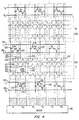
- Fig. 2 illustrates the architecture of a memory device according to one preferred embodiment of the present invention.
- the two-dimensional array is partitioned into segmented arrays (such as 100, 110).
- each segmented array consists of 16 or 32 rows of cells.
- a two-dimensional array with a total of 1024 rows may be partitioned into 32 segments each consisting of 32 rows.
- the bit line is also partitioned into 32 independent bit-line segments.
- the X-addressing can be done, by row decoding the word lines across the segmented arrays in the two-dimensional array, similar to the conventional case illustrated in Fig. 1.
- an absolute row address can be given by a segmented array address and a local row address in the segment, and be decoded appropriately.
- the X-address is given by the address of the segmented array 100 together with the local address of the word line 122.
- the local address of the word line 122 is the second word line in the segment.
- the decoding is straight forward and is not shown in Fig. 2 so as not to overburden the illustration.
- the Y-addressing must connect the pair of bit lines in an addressed column of an addressed segmented array to the corresponding pair of conductive strip or metal lines.
- its pair of bit lines 124, 126 must be connected to a pair of corresponding metal lines, namely 134, 136.
- the pair of metal lines 134, 136 in turn are connected to a sense amplifier circuit (not shown) via a column decoder 140.
- a segment-select transistor 150 is used to selectively connect the segmented bit line 124 to the corresponding metal line 134. The connection is made to the metal line 134 via a metal contact 142. Whenever a logical HIGH signal appears at a select line 151 connected to the control gate of the segment-select transistor 150, the transistor is turned on. Similarly, a HIGH signal appearing at the select line 161 connected to the control gate of a segment-select transistor 160 selectively connects the segmented bit line 126 to the corresponding metal line 136. Thus, when the cell 120 is being addressed, both select lines 151, 161 controlling the cell's source and drain line respectively are pulled HIGH, thereby connecting them to the metal lines 134, 136 respectively.
- a novel feature of the invention is that the configuration of the segment-select transistors allows them to have double the pitch of the columns. Therefore the transistors can have double the size compared to one transistor per column, thereby increasing their current capacity and reducing the programming path resistance.
- This is essential for programmable memory devices such as EPROM or Flash EEPROM, where the drain-source current during programming is one or two orders of magnitude greater than that during reading. Segmentation introduces segment-select transistors which increase the resistance in the programming path through the segment select transistor which causes a potential difference across said transistor and consequent reduction in programming efficiency.
- the series resistance path during programming is the combination of the two segment-select transistors (one on the drain bit line, one on the source bit line) and the source and drain buried diffusion bit line resistance.
- the segmented array 100 has segment-select transistors 150, 152, 154, ... connected to the odd bit lines from above and segment-select transistors 160, 162, 164, ... connected to the even bit lines from below.
- the configurations of the adjacent segmented arrays are reversed.
- the segmented array 110 below the segmented array 100 has segment-select transistors 170, 172, 174, ... connected to the even bit lines from above and segment-select transistors 180, 182, 184, ... connected to the odd bit lines from below.
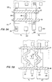
- Fig. 3 is a schematic physical layout of the segment-select transistor such as the transistor 150 illustrated in Fig. 2.
- the segment-select transistor has its source connected to the bit line 124, and its drain connected to the metal contact 142. Its gate 151 runs horizontal and joins onto that of other segment-select transistors in alternate columns.
- the metal line 134 overlays the bit line 124, and the adjacent metal line 136 overlays the bit line 126.
- segmented architecture of the present invention there are several other advantages to the segmented architecture of the present invention. For example, by breaking an array with 1026 rows into 32 segmented arrays each consisting of 32 rows, many column-dependent undesirable effects are also significantly reduced by 32 times.
- bit line series resistance For example, for the flash EEPROM cell with dimension of 2.6x3.0 ⁇ 2 , the source-drain resistance is equal to about 60 ⁇ per cell.
- the bit-line resistance for each 32-row segmented array is reduced 32 times compared to a non-segmented array and only ranges from ⁇ 100 ⁇ to a maximum of ⁇ 2k ⁇ .
- One advantage of this is the possibility of using metal contacts in between segments every 32 rows rather than within the arrays. This makes contacts easier and fewer, thereby increasing reliability.
- the negative side of this will be more programming sensitivity to location along the 32 rows in a segmented array. Owing to the cumulative series resistance along a bit line, some rows may be slower to program than others. This will limit the maximum number of rows in each segmented array. For example, the worst case diffusion resistance on the drain side for a cell 32 rows away from the nearest segment select transistor is ⁇ 2000 ⁇ . This is still within the acceptable range for effective programming.
- column capacitance is also reduced by a factor of 32 (from ⁇ 10pF to ⁇ 0.3pF).
- the metal line capacitance is also reduced by a factor of 5 - 10 times, allowing fast sense fast precharge and smaller power spike as a result of charging or discharging bit lines. This will save much power during program column precharge/discharge.
- Segmentation also reduces sensitivity to defects. Any defect located within a segment is isolated to that segment. There is almost no possibility for local latent defects to propagate beyond their segment. Any short between word lines, erase gates, and buried diffusions; bit-line to bit-line shorts, punchthrough, or high background leakage, can be entirely contained to a segment. This enables a system which can remap defective segments to working segments to eliminate otherwise catastrophic column defects.
- Bit-line to bit-line leakage is reduced by 32 times and may be tolerable.
- Program disturb is reduced by 32 times (only one segment at a time is exposed to the bit line drain voltage).
- Reverse program disturb is greatly reduced because of the series source select transistor.
- Fig. 4 illustrates an alternative segmentation in which the segment-select transistors are arranged differently from that of Fig. 2.
- This architecture has the further advantages of allowing the segment-select transistors to have 4 times the pitch of the bit lines, and the metal lines to have double the pitch of the bit lines.
- Each segmented array preferably consists of 32 or 64 rows of cells.
- Segment-select transistors (such as 222, 224, 226, 228, ...; 232, 234, 236, 238, ...) are used to connect a metal line (such as m 1 , m 2 , m 3 , ...) to the bit lines (such as 241, 242, 243, 244, %) in the columns (such as 251, 252, 253, ).
- the first metal line m 1 is connectable via a metal contact 261 and segment-select transistors 222, 224 to the bit lines 241, 243.
- the metal line m 2 is connectable via a metal contact 262 and segment-select transistors 232, 234 to the bit lines 242, 244.
- each of two adjacent alternate bit lines are served by a single metal line, which is decoded either to the left bit line or to the right bit line.
- the metal lines m 1 , m 2 , ... are in turned decoded by a metal line decoder 292 and connected to the source and drain voltages.
- L 1 , L 2 , R 1 and R 2 are respectively 281, 283, 282 and 284. If the cell 272 is to be programmed to the state "1", the following conditions are applied:
- the cells 271, 273 to the left and right of the cell 272 are not affected.
- the cell 271 (to the left of the cell 272) has:
- V drain OV
- the cell 273 (to the right of the cell 272) has:
- Fig. 5A illustrates one embodiment of a physical layout of the segment-select transistors 222, 224 shown in Fig. 4.
- the metal line m 1 overlies the bit lines 241, 242, and m 2 overlies the bit lines 243, 244.
- Both transistors 222 and 224 have their drain connected to the metal contact 261.
- the source of the transistor 222 is connected to the bit line 241 with the aid of a jumper 293 so that the alternate, in-line segmented bit lines of adjacent segmented array (such as 200, 210) are connected.
- the source of the transistor 224 is connected to the bit line 243 which is also linked to the one in the adjacent segmented array with the aid of a jumper 295.
- the gate 271 of the transistor 222 forms part of the L 1 select line which runs horizontally and joins onto the gate of other segment-select transistors. Similar, the gate 281 of the transistor 224 forms part of the R 1 select line.
- Fig. 5B shows an alternative layout which does not require jumpers for connecting alternate bit lines between adjacent segmented arrays.
- the source and drain of the segment select transistors are rotated at right angle relative to that in Fig. 5A.
- Figs. 4, 5A and 5B The architecture of Figs. 4, 5A and 5B is advantageous over that of Figs. 2 and 3 in several ways.
- First is the doubling of the metal line pitch relative to the bit lines. With only one metal line per two bit lines, the metal lines can be made wider and further apart, thereby significantly improving yield.
- the segment-select transistors can be made more than twice as wide. This is because two segment-select transistors fit in the pitch of 4 bit lines compared to that of 2 bit lines in Figs. 2 and 3. This is especially important for programmable memory devices such as EPROM and Flash EEPROM.
- the larger segment-select transistor provides low "on resistance" during programming of the selected segment.
- Third, the number of metal contacts is further reduced to 1 contact per 128 cells (for a 32-row segmented array).
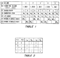
- Table 1(a)-(g) summarize the decoding scheme for the alternative embodiment.
- Table 1(a) the columns 1, 2, 3, ... correspond to that labelled by numerals 251, 252, 253, ... illustrated in Fig. 4.
- Table 1(b) shows the binary Y-address assigned to the columns.
- Table 1(c) distinguish between the source and drain line for each cell in each column.
- Table 1(d) shows the corresponding conductive strip or metal line connectable to the source or drain bit lines.
- Table 1(e) lists the select lines which must be selected for the appropriate segment-select transistor.
- Fig. 6A illustrates a select-line decoding scheme which will decode according to Table 1(e).
- the columns structure illustrated in Fig. 4 exhibits a periodicity of 4. In each period, the four column addresses are encoded by the last two binary digits Y(1), Y(0) of the column address (see Table 1(b)).
- a decoding circuit 300 takes Y(0), Y(1) as inputs and decodes according to that shown in Table 2, which is consistent with the requirements of Table 1(e).
- Fig. 6B illustrates an X-decoder 310 which in combination with the scheme of Fig. 6A selectively enable a given segmented array.
- the X-addressing can be split into addressing each segmented array and addressing the rows therein.
- the X-decoder 310 can similarly be regarded as comprising a segment decode portion 312 and a segment word line decode portion 314.
- the segment decode portion 312 has decoded lines such as SE 1 , SE 2 , .... They are used for enabling the corresponding segmented arrays 210, 320, ... (see Fig. 6A) via enabling transistors 331, 332, 333, 334, .... In this way, only the addressed segmented array is enabled.
- Fig. 7A illustrates a circuit for the metal line decoder 292 illustrated in Fig. 4.
- Each of the metal lines m 1 , m 2 , ... are connectable via enabling transistors such as 401, 402, 403 to either a node A 410 or a node B 420.
- the connections for the nodes A and B are interchanged from one column to another.
- Fig. 7B illustrates a circuit for decoding the enabling signals for the metal lines connections of Fig. 7A. Essentially, it ensures the matching of Table 1(a) with Table 1(c) and Table 1(d).
- the Y-address minus the last two binary digits is used to decode a first set of alternate metal lines (such as ME 1 , ME 3 , ME 5 , ).
- the last two binary digits of the Y-address Y(0), Y(1) are used to decode a second set of alternate metal lines (such as ME 2 , ME 4 , ME 6 , ...) from the first set.
- the column segmentation approach can be applied with similar advantages to other memory arrays. Specifically it can be used in conjunction with large capacity DRAM memories, where bit line capacitance can be reduced significantly, thereby eliminating the need for local sense amplifiers. It can equally well be employed in high capacity memory arrays of ROM and EEPROM.
Landscapes
- Engineering & Computer Science (AREA)
- Microelectronics & Electronic Packaging (AREA)
- Read Only Memory (AREA)
- Semiconductor Memories (AREA)
- Non-Volatile Memory (AREA)
Claims (12)
- Integrierte EPROM- oder EEPROM- oder Flash-EEPROM-Speicherschaltungsvorrichtung mit einer zweidimensionalen Matrix aus Speicherzellen (10), die in Reihen und Spalten organisiert sind, von denen jede Speicherzelle (20) eine Gateelektrode (26), eine Sourceelektrode (22), eine Drainelektrode (24) hat, wobei die zweidimensionale Matrix eine Wortleitung (40, 42) hat, die mit allen Gates in jeder Reihe verbunden ist, wobei die integrierte Speicherschaltungsvorrichtung ferner folgendes aufweist:dadurch gekennzeichnet, daßeine Vielzahl von Matrixsegmenten (100, 110), die durch Unterteilen der zweidimensionalen Matrix längs der Spaltenrichtung gebildet sind, wobei jedes Matrixsegment von einem Bereich segmentierter Spalten gebildet ist und jede segmentierte Spalte ein Paar unabhängiger, segmentierter Bitleitungen (124, 126) hat, mit dazwischen angeschlossenen Speicherzellen, so daß jedes Matrixsegment Spalte für Spalte durch eine Matrix der segmentierten Bitleitungen adressierbar ist;Zellzugriffsmittel, die mit einer adressierten Zelle in einem Matrixsegment durch die Wortleitung (122) und das damit verbundene Paar segmentierter Bitleitungen (124, 126) verbindbar sind, wobei die Zellzugriffsmittel ferner folgendes aufweisen:eine Vielzahl elektrisch isolierter, leitfähiger Schienen (134, 136) parallel zu den Spalten der zweidimensionalen Matrix und diesen überlagert, so daß für jede segmentierte Spalte darin das Paar segmentierter Bitleitungen derselben einem entsprechenden Paar der leiffähigen Schienen zum Zugriff durch dieselben zugeordnet ist;erste und zweite Schalttransistoren (150, 160) zum exklusiven und schaltbaren Verbinden des Paares segmentierter Bitleitungen mit dem Paar entsprechender, leitfähiger Schienen;jeder erste Schalttransistor am oberen Ende jeder segmentierten Spalte angeordnet ist, um eine erste Leitung des Paares segmentierter Bitleitungen mit einer ersten Schiene des Paares entsprechender leitfähiger Schienen zu verbinden; undjeder zweite Schalttransistor an einem unteren Ende jeder segmentierten Spalte angeordnet ist, um eine zweite Leitung des Paares segmentierter Bitleitungen mit einer zweiten Schiene des Paares entsprechender leitfähiger Schienen zu verbinden;wodurch in jedem Matrixsegment (100) eine Reihe der ersten Schalttransistoren (150, 152, 154, ...) an einem oberen Ende derselben in eins-zu-eins-Verbindung mit einem Satz abwechselnder, segmentierter Bitleitungen darin, und eine Reihe der zweiten Schalttransistoren (160, 162, 164, ...) an einem unteren Ende derselben in einer eins-zu-eins-Verbindung mit einem komplementären Satz abwechselnder, segmentierter Bitleitungen darin gebildet wird, wobei jede der Reihen der ersten oder zweiten Schalttransistoren einen Mittenabstand hat, der doppelt so groß ist wie der der Matrix der segmentierten Bitleitungen.
- Integrierte Speicherschaltungsvorrichtung nach Anspruch 1, bei der zum Zellzugriffsmittel ferner folgendes gehört:ein Kontaktpolster (142) für jeden der ersten und zweiten Schalttransistoren zum Anschluß an eine entsprechende leitfähige Schiene, um dadurch erste und zweite Reihen von Kontaktpolstern am oberen bzw. unteren Ende jedes Matrixsegmentes zu bilden, die jeweils einen Mittenabstand entsprechend dem der Reihe aus ersten oder zweiten Schalttransistoren haben.
- Integrierte Speicherschaltungsvorrichtung nach Anspruch 1, bei der:jedes Matrixsegment eine Speichermatrix mit virtueller Masse ist, in der längs jeder Reihe derselben die Speicherzellen dadurch seriell miteinander verbunden sind, daß die Drainelektrode einer Speicherzelle mit der Sourceelektrode einer anderen, ihr benachbarten Speicherzelle verbunden ist, so daß eine mit allen Drainelektroden einer segmentierten Spalte verbundene segmentierte Bitleitung mit derjenigen zusammenfällt, die mit allen Sourceelektroden einer anderen, ihr benachbarten segmentierten Spalte verbunden ist, und daß für jedes Matrixsegment die darin enthaltenen segmentierten Bitleitungen einen Mittenabstand entsprechend dem des Bereichs segmentierter Spalten derselben hat.
- Integrierte Speicherschaltungsvorrichtung nach Anspruch 3, bei der zum Zellzugriffsmittel ferner folgendes gehört:ein Kontaktpolster (142) für jeden der ersten und zweiten Schalttransistoren zum Anschluß an eine entsprechende leitfähige Schiene, um dadurch erste und zweite Reihen von Kontaktpolstern am oberen bzw. unteren Ende jedes Matrixsegmentes zu bilden, die jeweils einen Mittenabstand entsprechend dem der Reihe aus ersten oder zweiten Schalttransistoren haben.
- Integrierte Speicherschaltungsvorrichtung nach Anspruch 4, bei der die Vielzahl leitfähiger Schienen der Matrix der segmentierten Bitleitungen in der zweidimensionalen Matrix eins-zu-eins entsprechen, wodurch sie einen Mittenabstand haben, der dem der Matrix segmentierter Bitleitungen gleicht.
- Integrierte Speicherschaltungsvorrichtung nach Anspruch 4, wobei die Vielzahl der Matrixsegmente längs der Spaltenrichtung so angeordnet ist, daß sie die zweidimensionale Matrix bilden, und jedes Matrixsegment darin ein oberes Ende und ein unteres Ende desselben hat, bei der:zwischen jedem Paar benachbarter Matrixsegmente darin, wobei ein erstes des Paares unmittelbar unterhalb eines zweiten des Paares ist, die erste Reihe der Kontaktpolster am oberen Ende des ersten mit der zweiten Reihe Kontaktpolster am unteren Ende des zweiten zusammenfällt.
- Integrierte Speicherschaltungsvorrichtung nach Anspruch 4, bei der:die Vielzahl leiffähiger Schienen einen Mittenabstand haben, der doppelt so groß ist wie der der segmentierten Bitleitungen eines Matrixsegmentes.
- Integrierte Speicherschaltungsvorrichtung nach Anspruch 7, wobei die Vielzahl der Matrixsegmente längs der Spaltenrichtung so angeordnet ist, daß sie die zweidimensionale Matrix bilden, so daß die segmentierten Bitleitungen in jedem Matrixsegment mit denen der entsprechenden segmentierten Bitleitungen anderer Matrixsegmente in der zweidimensionalen Matrix fluchten, und jedes Matrixsegment darin ein oberes Ende und ein unteres Ende desselben hat, bei der:für jede Gruppe aus drei Matrixsegmenten darin, die aus einem unteren, einem mittleren und einem oberen Matrixsegment besteht, die segmentierten Bitleitungen des mittleren Matrixsegmentes abwechselnd mit denen der entsprechenden segmentierten Bitleitungen des oberen Matrixsegmentes und den unteren Matrixsegmenten am zweiten Transistor verbunden sind, um einen Satz sattelartiger, segmentierter Bitleitungen zu bilden.
- Integrierte Speicherschaltungsvorrichtung nach Anspruch 8, bei der:der Satz sattelartiger, segmentierter Bitleitungen aus ersten und zweiten Sätzen verschachtelter, sattelartiger, segmentierter Bitleitungen gebildet ist, wobei der erste Satz verschachtelter, sattelartiger, segmentierter Bitleitungen von jeder anderen sattelartigen, segmentierten Bitleitungen im vollen Satz sattelartiger, segmentierter Bitleitungen gebildet ist und der zweite Satz verschachtelter, sattelartiger, segmentierter Bitleitungen vom Komplement des ersten Satzes zwischengeschichteter, segmentierter Bitleitungen in dem vollen Satz sattelartiger, segmentierter Bitleitungen gebildet ist unddie ersten und zweiten Sätze verschachtelter, sattelartiger, segmentierter Bitleitungen jeweils zu Paaren gruppiert sind, wobei sich jedes Paar eine entsprechende leitfähige Schiene für die sattelartigen, segmentierten Bitleitungen darin teilt, um unabhängig und schaltbar damit verbindbar.
- Verfahren zum Segmentieren einer zweidimensionalen Matrix aus Speicherzellen in einer integrierten EPROM oder EEPROM oder Flash-EEPROM Speicherschaltungsvorrichtung, wobei die zweidimensionale Matrix in Reihen und Spalten organisiert ist, jede Speicherzelle eine Gateelektrode, eine Sourceelektrode und eine Drainelektrode hat, die zweidimensionale Matrix eine Wortleitung hat, die mit allen Gates in jeder Reihe verbunden ist, welches folgendes aufweist:Ausstatten des Zellzugriffsmittels mitUnterteilen der zweidimensionalen Matrix längs der Spaltenrichtung zu Schaffung einer Vielzahl von Matrixsegmenten (100, 110), wobei jedes Matrixsegment von einer Gruppe segmentierter Spalten gebildet ist und jede segmentierte Spalte ein Paar unabhängiger, segmentierter Bitleitungen (124, 126) hat, mit dazwischen angeschlossenen Speicherzellen, so daß jedes Matrixsegment Spalte für Spalte von einer Matrix segmentierter Bitleitungen adressierbar ist;wahlweises Verbinden eines Zellzugriffsmittels mit einer adressierten Zelle in einem Matrixsegment durch die Wortleitung und das Paar mit ihr verbundener segmentierter Bitleitungen,gekennzeichnet durcheiner Vielzahl elektrisch isolierter leiffähiger Schienen (134, 136), parallel zu den Spalten der zweidimensionalen Matrix und diesen überlagert, so daß für jede segmentierte Spalte darin das Paar segmentierter Bitleitungen derselben einem entsprechenden Paar der leiffähigen Schienen zum Zugriff durch dieselben zugeordnet ist;ersten und zweiten Schalttransistoren (151, 161) zum ausschließlichen und schaltbaren Verbinden des Paares segmentierter Bitleitungen mit dem Paar entsprechender leitfähiger Schienen;Anordnen jedes ersten Schalttransistors (151) an einem oberen Ende jeder segmentierten Spalte zum schaltbaren Verbinden einer ersten Leitung des Paares segmentierter Bitleitungen mit einer ersten Schiene des Paares entsprechender leitfähiger Schienen; undAnordnen jedes zweiten Schalttransistors (161) an einem unteren Ende jeder segmentierten Spalte zum schaltbaren Verbinden einer zweiten Leitung des Paares segmentierter Bitleitungen mit einer zweiten Schiene des Paares entsprechender leitfähiger Schienen;wodurch in jedem Matrixsegment eine Reihe der ersten Schalttransistoren an einem oberen Ende derselben in einer eins-zu-eins-Verbindung mit einem Satz abwechselnder segmentierter Bitleitungen darin und eine Reihe der zweiten Schalttransistoren an einem unteren Ende derselben in einer eins-zu-eins-Verbindung mit einem komplementären Satz abwechselnder segmentierter Bitleitungen darin geschaffen wird, wobei jede Reihe der ersten oder zweiten Schalttransistoren einen Mittenabstand hat, der dem Doppelten der Matrix segmentierter Bitleitungen entspricht.
- Verfahren nach Anspruch 10, bei dem die Verbesserung das Isolieren von möglicherweise in einem Segment auftretenden Defekten dadurch aufweist, daß die zweidimensionale Matrix so segmentiert ist, daß eine segmentierte Spalte darin, die einen Defekt enthält, darin isoliert wird.
- Verfahren nach Anspruch 10, bei dem die Verbesserung das Reduzieren der Kapazität in der Source- und Drainelektrode einer adressierten Speicherzelle dadurch aufweist, daß die zweidimensionale Matrix Matrixsegmente mit unabhängigen segmentierten Bitleitungen hat, daß von anderen segmentierten Bitleitungen vermittelte zusätzliche Kapazität vermieden wird.
Applications Claiming Priority (2)
| Application Number | Priority Date | Filing Date | Title |
|---|---|---|---|
| US07/919,715 US5315541A (en) | 1992-07-24 | 1992-07-24 | Segmented column memory array |
| US919715 | 1992-07-24 |
Publications (3)
| Publication Number | Publication Date |
|---|---|
| EP0580467A2 EP0580467A2 (de) | 1994-01-26 |
| EP0580467A3 EP0580467A3 (en) | 1994-08-24 |
| EP0580467B1 true EP0580467B1 (de) | 1998-09-02 |
Family
ID=25442525
Family Applications (1)
| Application Number | Title | Priority Date | Filing Date |
|---|---|---|---|
| EP93401631A Expired - Lifetime EP0580467B1 (de) | 1992-07-24 | 1993-06-25 | Speichermatrix mit segmentierten Spalten |
Country Status (4)
| Country | Link |
|---|---|
| US (1) | US5315541A (de) |
| EP (1) | EP0580467B1 (de) |
| JP (1) | JP3744551B2 (de) |
| DE (1) | DE69320733T2 (de) |
Cited By (26)
| Publication number | Priority date | Publication date | Assignee | Title |
|---|---|---|---|---|
| US6282145B1 (en) | 1999-01-14 | 2001-08-28 | Silicon Storage Technology, Inc. | Array architecture and operating methods for digital multilevel nonvolatile memory integrated circuit system |
| US6285598B1 (en) | 1997-03-06 | 2001-09-04 | Silicon Storage Technology, Inc. | Precision programming of nonvolatile memory cells |
| US7221138B2 (en) | 2005-09-27 | 2007-05-22 | Saifun Semiconductors Ltd | Method and apparatus for measuring charge pump output current |
| US7317633B2 (en) | 2004-07-06 | 2008-01-08 | Saifun Semiconductors Ltd | Protection of NROM devices from charge damage |
| US7352627B2 (en) | 2006-01-03 | 2008-04-01 | Saifon Semiconductors Ltd. | Method, system, and circuit for operating a non-volatile memory array |
| US7369440B2 (en) | 2005-01-19 | 2008-05-06 | Saifun Semiconductors Ltd. | Method, circuit and systems for erasing one or more non-volatile memory cells |
| US7405969B2 (en) | 1997-08-01 | 2008-07-29 | Saifun Semiconductors Ltd. | Non-volatile memory cell and non-volatile memory devices |
| US7420848B2 (en) | 2002-01-31 | 2008-09-02 | Saifun Semiconductors Ltd. | Method, system, and circuit for operating a non-volatile memory array |
| US7457183B2 (en) | 2003-09-16 | 2008-11-25 | Saifun Semiconductors Ltd. | Operating array cells with matched reference cells |
| US7466594B2 (en) | 2004-08-12 | 2008-12-16 | Saifun Semiconductors Ltd. | Dynamic matching of signal path and reference path for sensing |
| US7512009B2 (en) | 2001-04-05 | 2009-03-31 | Saifun Semiconductors Ltd. | Method for programming a reference cell |
| US7532529B2 (en) | 2004-03-29 | 2009-05-12 | Saifun Semiconductors Ltd. | Apparatus and methods for multi-level sensing in a memory array |
| US7605579B2 (en) | 2006-09-18 | 2009-10-20 | Saifun Semiconductors Ltd. | Measuring and controlling current consumption and output current of charge pumps |
| US7638835B2 (en) | 2006-02-28 | 2009-12-29 | Saifun Semiconductors Ltd. | Double density NROM with nitride strips (DDNS) |
| US7638850B2 (en) | 2004-10-14 | 2009-12-29 | Saifun Semiconductors Ltd. | Non-volatile memory structure and method of fabrication |
| US7668017B2 (en) | 2005-08-17 | 2010-02-23 | Saifun Semiconductors Ltd. | Method of erasing non-volatile memory cells |
| US7675782B2 (en) | 2002-10-29 | 2010-03-09 | Saifun Semiconductors Ltd. | Method, system and circuit for programming a non-volatile memory array |
| US7692961B2 (en) | 2006-02-21 | 2010-04-06 | Saifun Semiconductors Ltd. | Method, circuit and device for disturb-control of programming nonvolatile memory cells by hot-hole injection (HHI) and by channel hot-electron (CHE) injection |
| US7701779B2 (en) | 2006-04-27 | 2010-04-20 | Sajfun Semiconductors Ltd. | Method for programming a reference cell |
| US7738304B2 (en) | 2002-07-10 | 2010-06-15 | Saifun Semiconductors Ltd. | Multiple use memory chip |
| US7743230B2 (en) | 2003-01-31 | 2010-06-22 | Saifun Semiconductors Ltd. | Memory array programming circuit and a method for using the circuit |
| US7760554B2 (en) | 2006-02-21 | 2010-07-20 | Saifun Semiconductors Ltd. | NROM non-volatile memory and mode of operation |
| US7786512B2 (en) | 2005-07-18 | 2010-08-31 | Saifun Semiconductors Ltd. | Dense non-volatile memory array and method of fabrication |
| US7808818B2 (en) | 2006-01-12 | 2010-10-05 | Saifun Semiconductors Ltd. | Secondary injection for NROM |
| US8053812B2 (en) | 2005-03-17 | 2011-11-08 | Spansion Israel Ltd | Contact in planar NROM technology |
| US8253452B2 (en) | 2006-02-21 | 2012-08-28 | Spansion Israel Ltd | Circuit and method for powering up an integrated circuit and an integrated circuit utilizing same |
Families Citing this family (502)
| Publication number | Priority date | Publication date | Assignee | Title |
|---|---|---|---|---|
| US5719806A (en) * | 1991-02-18 | 1998-02-17 | Yamane; Masatoshi | Memory cell array |
| US6222762B1 (en) * | 1992-01-14 | 2001-04-24 | Sandisk Corporation | Multi-state memory |
| US7071060B1 (en) | 1996-02-28 | 2006-07-04 | Sandisk Corporation | EEPROM with split gate source side infection with sidewall spacers |
| US5618742A (en) * | 1992-01-22 | 1997-04-08 | Macronix Internatioal, Ltd. | Method of making flash EPROM with conductive sidewall spacer contacting floating gate |
| US5526307A (en) * | 1992-01-22 | 1996-06-11 | Macronix International Co., Ltd. | Flash EPROM integrated circuit architecture |
| US5657332A (en) * | 1992-05-20 | 1997-08-12 | Sandisk Corporation | Soft errors handling in EEPROM devices |
| US6549974B2 (en) * | 1992-06-22 | 2003-04-15 | Hitachi, Ltd. | Semiconductor storage apparatus including a controller for sending first and second write commands to different nonvolatile memories in a parallel or time overlapped manner |
| US5592415A (en) * | 1992-07-06 | 1997-01-07 | Hitachi, Ltd. | Non-volatile semiconductor memory |
| JP3474614B2 (ja) * | 1993-12-14 | 2003-12-08 | マクロニクス インターナショナル カンパニイ リミテッド | 不揮発性半導体メモリ装置及びその動作方法 |
| US5436478A (en) * | 1994-03-16 | 1995-07-25 | National Semiconductor Corporation | Fast access AMG EPROM with segment select transistors which have an increased width |
| KR100477034B1 (ko) | 1995-01-31 | 2005-03-21 | 가부시끼가이샤 히다치 세이사꾸쇼 | 반도체 메모리 장치 |
| WO1996041346A1 (en) * | 1995-06-07 | 1996-12-19 | Macronix International Co., Ltd. | Automatic programming algorithm for page mode flash memory with variable programming pulse height and pulse width |
| US5621697A (en) * | 1995-06-23 | 1997-04-15 | Macronix International Co., Ltd. | High density integrated circuit with bank select structure |
| JP3782840B2 (ja) * | 1995-07-14 | 2006-06-07 | 株式会社ルネサステクノロジ | 外部記憶装置およびそのメモリアクセス制御方法 |
| US5838614A (en) * | 1995-07-31 | 1998-11-17 | Lexar Microsystems, Inc. | Identification and verification of a sector within a block of mass storage flash memory |
| US8171203B2 (en) * | 1995-07-31 | 2012-05-01 | Micron Technology, Inc. | Faster write operations to nonvolatile memory using FSInfo sector manipulation |
| US6081878A (en) | 1997-03-31 | 2000-06-27 | Lexar Media, Inc. | Increasing the memory performance of flash memory devices by writing sectors simultaneously to multiple flash memory devices |
| US5845313A (en) * | 1995-07-31 | 1998-12-01 | Lexar | Direct logical block addressing flash memory mass storage architecture |
| US6801979B1 (en) | 1995-07-31 | 2004-10-05 | Lexar Media, Inc. | Method and apparatus for memory control circuit |
| US6728851B1 (en) | 1995-07-31 | 2004-04-27 | Lexar Media, Inc. | Increasing the memory performance of flash memory devices by writing sectors simultaneously to multiple flash memory devices |
| US6978342B1 (en) | 1995-07-31 | 2005-12-20 | Lexar Media, Inc. | Moving sectors within a block of information in a flash memory mass storage architecture |
| US6757800B1 (en) | 1995-07-31 | 2004-06-29 | Lexar Media, Inc. | Increasing the memory performance of flash memory devices by writing sectors simultaneously to multiple flash memory devices |
| US5687114A (en) | 1995-10-06 | 1997-11-11 | Agate Semiconductor, Inc. | Integrated circuit for storage and retrieval of multiple digital bits per nonvolatile memory cell |
| WO1997032253A1 (fr) * | 1996-02-29 | 1997-09-04 | Hitachi, Ltd. | Dispositif de memoire a semi-conducteur presentant des cellules defaillantes |
| US5793079A (en) * | 1996-07-22 | 1998-08-11 | Catalyst Semiconductor, Inc. | Single transistor non-volatile electrically alterable semiconductor memory device |
| US5798968A (en) * | 1996-09-24 | 1998-08-25 | Sandisk Corporation | Plane decode/virtual sector architecture |
| US5777922A (en) * | 1996-10-18 | 1998-07-07 | Hyudai Electronics Industries Co., Ltd. | Flash memory device |
| EP0851426A3 (de) * | 1996-12-27 | 1999-11-24 | STMicroelectronics S.r.l. | Speicherblock zur Realisierung von Halbleiterspeicheranordnungen und entsprechendes Herstellungsverfahren |
| JP2000504504A (ja) * | 1997-02-12 | 2000-04-11 | ヒュンダイ エレクトロニクス アメリカ インコーポレイテッド | 不揮発性メモリ構造 |
| US6487116B2 (en) | 1997-03-06 | 2002-11-26 | Silicon Storage Technology, Inc. | Precision programming of nonvolatile memory cells |
| US6034897A (en) * | 1999-04-01 | 2000-03-07 | Lexar Media, Inc. | Space management for managing high capacity nonvolatile memory |
| US6122195A (en) * | 1997-03-31 | 2000-09-19 | Lexar Media, Inc. | Method and apparatus for decreasing block write operation times performed on nonvolatile memory |
| US6411546B1 (en) | 1997-03-31 | 2002-06-25 | Lexar Media, Inc. | Nonvolatile memory using flexible erasing methods and method and system for using same |
| KR100252475B1 (ko) * | 1997-05-24 | 2000-04-15 | 윤종용 | 반도체 롬 장치 |
| US6633496B2 (en) | 1997-12-12 | 2003-10-14 | Saifun Semiconductors Ltd. | Symmetric architecture for memory cells having widely spread metal bit lines |
| US5963465A (en) | 1997-12-12 | 1999-10-05 | Saifun Semiconductors, Ltd. | Symmetric segmented memory array architecture |
| US6633499B1 (en) | 1997-12-12 | 2003-10-14 | Saifun Semiconductors Ltd. | Method for reducing voltage drops in symmetric array architectures |
| US6430077B1 (en) * | 1997-12-12 | 2002-08-06 | Saifun Semiconductors Ltd. | Method for regulating read voltage level at the drain of a cell in a symmetric array |
| GB9801373D0 (en) | 1998-01-22 | 1998-03-18 | Memory Corp Plc | Memory system |
| ITMI981123A1 (it) * | 1998-05-21 | 1999-11-21 | Sgs Thomson Microelectronics | Metodo processo e dispositivo per l'individuazione di difetti puntuali che provocano correnti di leakage in un dispositivo di memoria non |
| KR100316060B1 (ko) * | 1998-06-16 | 2002-02-19 | 박종섭 | 플래시메모리의레이아웃및그형성방법 |
| WO2000030116A1 (en) | 1998-11-17 | 2000-05-25 | Lexar Media, Inc. | Method and apparatus for memory control circuit |
| JP3244067B2 (ja) * | 1998-11-26 | 2002-01-07 | 日本電気株式会社 | 不揮発性半導体記憶装置とその製造方法 |
| US6141249A (en) * | 1999-04-01 | 2000-10-31 | Lexar Media, Inc. | Organization of blocks within a nonvolatile memory unit to effectively decrease sector write operation time |
| EP1729304B1 (de) | 1999-04-01 | 2012-10-17 | Lexar Media, Inc. | Platzverwaltung zur Verwaltung eines nichtflüchtigen Hochleistungsspeichers |
| US6125057A (en) * | 1999-06-21 | 2000-09-26 | Lucent Technologies Inc. | Segmented source memory array |
| US6103573A (en) * | 1999-06-30 | 2000-08-15 | Sandisk Corporation | Processing techniques for making a dual floating gate EEPROM cell array |
| US6151248A (en) | 1999-06-30 | 2000-11-21 | Sandisk Corporation | Dual floating gate EEPROM cell array with steering gates shared by adjacent cells |
| US6163489A (en) * | 1999-07-16 | 2000-12-19 | Micron Technology Inc. | Semiconductor memory having multiple redundant columns with offset segmentation boundaries |
| US6091633A (en) * | 1999-08-09 | 2000-07-18 | Sandisk Corporation | Memory array architecture utilizing global bit lines shared by multiple cells |
| US7102671B1 (en) | 2000-02-08 | 2006-09-05 | Lexar Media, Inc. | Enhanced compact flash memory card |
| US6426893B1 (en) | 2000-02-17 | 2002-07-30 | Sandisk Corporation | Flash eeprom system with simultaneous multiple data sector programming and storage of physical block characteristics in other designated blocks |
| US6396741B1 (en) * | 2000-05-04 | 2002-05-28 | Saifun Semiconductors Ltd. | Programming of nonvolatile memory cells |
| US6928001B2 (en) | 2000-12-07 | 2005-08-09 | Saifun Semiconductors Ltd. | Programming and erasing methods for a non-volatile memory cell |
| US6567307B1 (en) | 2000-07-21 | 2003-05-20 | Lexar Media, Inc. | Block management for mass storage |
| US7167944B1 (en) | 2000-07-21 | 2007-01-23 | Lexar Media, Inc. | Block management for mass storage |
| US7113432B2 (en) * | 2000-09-14 | 2006-09-26 | Sandisk Corporation | Compressed event counting technique and application to a flash memory system |
| US6345001B1 (en) | 2000-09-14 | 2002-02-05 | Sandisk Corporation | Compressed event counting technique and application to a flash memory system |
| US6512263B1 (en) * | 2000-09-22 | 2003-01-28 | Sandisk Corporation | Non-volatile memory cell array having discontinuous source and drain diffusions contacted by continuous bit line conductors and methods of forming |
| US6538922B1 (en) | 2000-09-27 | 2003-03-25 | Sandisk Corporation | Writable tracking cells |
| US6542396B1 (en) * | 2000-09-29 | 2003-04-01 | Artisan Components, Inc. | Method and apparatus for a dense metal programmable ROM |
| US6477083B1 (en) * | 2000-10-11 | 2002-11-05 | Advanced Micro Devices, Inc. | Select transistor architecture for a virtual ground non-volatile memory cell array |
| US6684289B1 (en) | 2000-11-22 | 2004-01-27 | Sandisk Corporation | Techniques for operating non-volatile memory systems with data sectors having different sizes than the sizes of the pages and/or blocks of the memory |
| JP2007200545A (ja) * | 2001-01-12 | 2007-08-09 | Renesas Technology Corp | 不揮発性半導体記憶装置 |
| US6614692B2 (en) | 2001-01-18 | 2003-09-02 | Saifun Semiconductors Ltd. | EEPROM array and method for operation thereof |
| US6677805B2 (en) * | 2001-04-05 | 2004-01-13 | Saifun Semiconductors Ltd. | Charge pump stage with body effect minimization |
| US6636440B2 (en) | 2001-04-25 | 2003-10-21 | Saifun Semiconductors Ltd. | Method for operation of an EEPROM array, including refresh thereof |
| US6894343B2 (en) * | 2001-05-18 | 2005-05-17 | Sandisk Corporation | Floating gate memory cells utilizing substrate trenches to scale down their size |
| US6936887B2 (en) * | 2001-05-18 | 2005-08-30 | Sandisk Corporation | Non-volatile memory cells utilizing substrate trenches |
| US6532172B2 (en) | 2001-05-31 | 2003-03-11 | Sandisk Corporation | Steering gate and bit line segmentation in non-volatile memories |
| JP3640177B2 (ja) * | 2001-06-04 | 2005-04-20 | セイコーエプソン株式会社 | 不揮発性半導体記憶装置 |
| US6480422B1 (en) | 2001-06-14 | 2002-11-12 | Multi Level Memory Technology | Contactless flash memory with shared buried diffusion bit line architecture |
| JP3622697B2 (ja) | 2001-07-23 | 2005-02-23 | セイコーエプソン株式会社 | 不揮発性半導体記憶装置 |
| JP3594001B2 (ja) | 2001-07-23 | 2004-11-24 | セイコーエプソン株式会社 | 不揮発性半導体記憶装置 |
| US6762092B2 (en) * | 2001-08-08 | 2004-07-13 | Sandisk Corporation | Scalable self-aligned dual floating gate memory cell array and methods of forming the array |
| US7177197B2 (en) | 2001-09-17 | 2007-02-13 | Sandisk Corporation | Latched programming of memory and method |
| US6985388B2 (en) * | 2001-09-17 | 2006-01-10 | Sandisk Corporation | Dynamic column block selection |
| US7170802B2 (en) * | 2003-12-31 | 2007-01-30 | Sandisk Corporation | Flexible and area efficient column redundancy for non-volatile memories |
| US6552932B1 (en) * | 2001-09-21 | 2003-04-22 | Sandisk Corporation | Segmented metal bitlines |
| GB0123416D0 (en) * | 2001-09-28 | 2001-11-21 | Memquest Ltd | Non-volatile memory control |
| GB0123410D0 (en) | 2001-09-28 | 2001-11-21 | Memquest Ltd | Memory system for data storage and retrieval |
| GB0123417D0 (en) | 2001-09-28 | 2001-11-21 | Memquest Ltd | Improved data processing |
| GB0123421D0 (en) * | 2001-09-28 | 2001-11-21 | Memquest Ltd | Power management system |
| GB0123412D0 (en) | 2001-09-28 | 2001-11-21 | Memquest Ltd | Memory system sectors |
| GB0123419D0 (en) | 2001-09-28 | 2001-11-21 | Memquest Ltd | Data handling system |
| GB0123415D0 (en) * | 2001-09-28 | 2001-11-21 | Memquest Ltd | Method of writing data to non-volatile memory |
| US6643181B2 (en) | 2001-10-24 | 2003-11-04 | Saifun Semiconductors Ltd. | Method for erasing a memory cell |
| US6897522B2 (en) | 2001-10-31 | 2005-05-24 | Sandisk Corporation | Multi-state non-volatile integrated circuit memory systems that employ dielectric storage elements |
| US6925007B2 (en) * | 2001-10-31 | 2005-08-02 | Sandisk Corporation | Multi-state non-volatile integrated circuit memory systems that employ dielectric storage elements |
| JP4087108B2 (ja) | 2001-12-10 | 2008-05-21 | シャープ株式会社 | 不揮発性半導体記憶装置及びその製造方法 |
| JP3998467B2 (ja) | 2001-12-17 | 2007-10-24 | シャープ株式会社 | 不揮発性半導体メモリ装置及びその動作方法 |
| US6885585B2 (en) * | 2001-12-20 | 2005-04-26 | Saifun Semiconductors Ltd. | NROM NOR array |
| US6950918B1 (en) | 2002-01-18 | 2005-09-27 | Lexar Media, Inc. | File management of one-time-programmable nonvolatile memory devices |
| US6957295B1 (en) | 2002-01-18 | 2005-10-18 | Lexar Media, Inc. | File management of one-time-programmable nonvolatile memory devices |
| US6975536B2 (en) | 2002-01-31 | 2005-12-13 | Saifun Semiconductors Ltd. | Mass storage array and methods for operation thereof |
| JP4082913B2 (ja) * | 2002-02-07 | 2008-04-30 | 株式会社ルネサステクノロジ | メモリシステム |
| US6871257B2 (en) | 2002-02-22 | 2005-03-22 | Sandisk Corporation | Pipelined parallel programming operation in a non-volatile memory system |
| US7231643B1 (en) | 2002-02-22 | 2007-06-12 | Lexar Media, Inc. | Image rescue system including direct communication between an application program and a device driver |
| US6795349B2 (en) * | 2002-02-28 | 2004-09-21 | Sandisk Corporation | Method and system for efficiently reading and programming of dual cell memory elements |
| US7221591B1 (en) | 2002-05-06 | 2007-05-22 | Samsung Electronics Co., Ltd. | Fabricating bi-directional nonvolatile memory cells |
| US6914820B1 (en) | 2002-05-06 | 2005-07-05 | Multi Level Memory Technology | Erasing storage nodes in a bi-directional nonvolatile memory cell |
| US6747896B2 (en) | 2002-05-06 | 2004-06-08 | Multi Level Memory Technology | Bi-directional floating gate nonvolatile memory |
| US6894930B2 (en) | 2002-06-19 | 2005-05-17 | Sandisk Corporation | Deep wordline trench to shield cross coupling between adjacent cells for scaled NAND |
| AU2003237515A1 (en) * | 2002-06-19 | 2004-01-06 | Sandisk Corporation | Deep wordline trench to shield cross coupling between adjacent cells for scaled nand |
| US6826107B2 (en) * | 2002-08-01 | 2004-11-30 | Saifun Semiconductors Ltd. | High voltage insertion in flash memory cards |
| US6987693B2 (en) | 2002-09-24 | 2006-01-17 | Sandisk Corporation | Non-volatile memory and method with reduced neighboring field errors |
| US6983428B2 (en) | 2002-09-24 | 2006-01-03 | Sandisk Corporation | Highly compact non-volatile memory and method thereof |
| US7327619B2 (en) * | 2002-09-24 | 2008-02-05 | Sandisk Corporation | Reference sense amplifier for non-volatile memory |
| US7046568B2 (en) * | 2002-09-24 | 2006-05-16 | Sandisk Corporation | Memory sensing circuit and method for low voltage operation |
| WO2004029984A2 (en) * | 2002-09-24 | 2004-04-08 | Sandisk Corporation | Non-volatile memory and its sensing method |
| US7196931B2 (en) * | 2002-09-24 | 2007-03-27 | Sandisk Corporation | Non-volatile memory and method with reduced source line bias errors |
| US7324393B2 (en) * | 2002-09-24 | 2008-01-29 | Sandisk Corporation | Method for compensated sensing in non-volatile memory |
| US6891753B2 (en) | 2002-09-24 | 2005-05-10 | Sandisk Corporation | Highly compact non-volatile memory and method therefor with internal serial buses |
| US7443757B2 (en) * | 2002-09-24 | 2008-10-28 | Sandisk Corporation | Non-volatile memory and method with reduced bit line crosstalk errors |
| US6940753B2 (en) | 2002-09-24 | 2005-09-06 | Sandisk Corporation | Highly compact non-volatile memory and method therefor with space-efficient data registers |
| US6908817B2 (en) * | 2002-10-09 | 2005-06-21 | Sandisk Corporation | Flash memory array with increased coupling between floating and control gates |
| US6901498B2 (en) | 2002-12-09 | 2005-05-31 | Sandisk Corporation | Zone boundary adjustment for defects in non-volatile memories |
| US6944063B2 (en) * | 2003-01-28 | 2005-09-13 | Sandisk Corporation | Non-volatile semiconductor memory with large erase blocks storing cycle counts |
| US7233024B2 (en) | 2003-03-31 | 2007-06-19 | Sandisk 3D Llc | Three-dimensional memory device incorporating segmented bit line memory array |
| US6879505B2 (en) * | 2003-03-31 | 2005-04-12 | Matrix Semiconductor, Inc. | Word line arrangement having multi-layer word line segments for three-dimensional memory array |
| US7045849B2 (en) * | 2003-05-21 | 2006-05-16 | Sandisk Corporation | Use of voids between elements in semiconductor structures for isolation |
| US7105406B2 (en) * | 2003-06-20 | 2006-09-12 | Sandisk Corporation | Self aligned non-volatile memory cell and process for fabrication |
| CN100362661C (zh) * | 2003-08-04 | 2008-01-16 | 旺宏电子股份有限公司 | 具对称性选择晶体管的快闪存储器 |
| US6956770B2 (en) * | 2003-09-17 | 2005-10-18 | Sandisk Corporation | Non-volatile memory and method with bit line compensation dependent on neighboring operating modes |
| US7064980B2 (en) * | 2003-09-17 | 2006-06-20 | Sandisk Corporation | Non-volatile memory and method with bit line coupled compensation |
| US7012835B2 (en) * | 2003-10-03 | 2006-03-14 | Sandisk Corporation | Flash memory data correction and scrub techniques |
| US7173852B2 (en) * | 2003-10-03 | 2007-02-06 | Sandisk Corporation | Corrected data storage and handling methods |
| US7221008B2 (en) * | 2003-10-06 | 2007-05-22 | Sandisk Corporation | Bitline direction shielding to avoid cross coupling between adjacent cells for NAND flash memory |
| US7301807B2 (en) | 2003-10-23 | 2007-11-27 | Sandisk Corporation | Writable tracking cells |
| CN1809833B (zh) | 2003-12-17 | 2015-08-05 | 雷克萨媒体公司 | 用于减少用于购买的电子设备的盗窃发生率的方法 |
| US7173863B2 (en) * | 2004-03-08 | 2007-02-06 | Sandisk Corporation | Flash controller cache architecture |
| US7433993B2 (en) * | 2003-12-30 | 2008-10-07 | San Disk Corportion | Adaptive metablocks |
| US7383375B2 (en) * | 2003-12-30 | 2008-06-03 | Sandisk Corporation | Data run programming |
| US7139864B2 (en) * | 2003-12-30 | 2006-11-21 | Sandisk Corporation | Non-volatile memory and method with block management system |
| US7631138B2 (en) | 2003-12-30 | 2009-12-08 | Sandisk Corporation | Adaptive mode switching of flash memory address mapping based on host usage characteristics |
| KR20070007265A (ko) | 2003-12-30 | 2007-01-15 | 쌘디스크 코포레이션 | 제어 데이터 관리를 구비한 비휘발성 메모리 및 방법 |
| US8504798B2 (en) | 2003-12-30 | 2013-08-06 | Sandisk Technologies Inc. | Management of non-volatile memory systems having large erase blocks |
| US20050251617A1 (en) * | 2004-05-07 | 2005-11-10 | Sinclair Alan W | Hybrid non-volatile memory system |
| US20050144363A1 (en) * | 2003-12-30 | 2005-06-30 | Sinclair Alan W. | Data boundary management |
| US7594135B2 (en) * | 2003-12-31 | 2009-09-22 | Sandisk Corporation | Flash memory system startup operation |
| EP1733555A4 (de) * | 2004-02-23 | 2009-09-30 | Lexar Media Inc | Sicherer kompakter flash |
| US7183153B2 (en) * | 2004-03-12 | 2007-02-27 | Sandisk Corporation | Method of manufacturing self aligned non-volatile memory cells |
| US7035129B1 (en) * | 2004-04-02 | 2006-04-25 | Virage Logic Corp. | Partitioned source line architecture for ROM |
| US7725628B1 (en) | 2004-04-20 | 2010-05-25 | Lexar Media, Inc. | Direct secondary device interface by a host |
| US7057939B2 (en) * | 2004-04-23 | 2006-06-06 | Sandisk Corporation | Non-volatile memory and control with improved partial page program capability |
| US7370166B1 (en) | 2004-04-30 | 2008-05-06 | Lexar Media, Inc. | Secure portable storage device |
| US7490283B2 (en) * | 2004-05-13 | 2009-02-10 | Sandisk Corporation | Pipelined data relocation and improved chip architectures |
| US8429313B2 (en) * | 2004-05-27 | 2013-04-23 | Sandisk Technologies Inc. | Configurable ready/busy control |
| US8375146B2 (en) * | 2004-08-09 | 2013-02-12 | SanDisk Technologies, Inc. | Ring bus structure and its use in flash memory systems |
| US20060036803A1 (en) * | 2004-08-16 | 2006-02-16 | Mori Edan | Non-volatile memory device controlled by a micro-controller |
| US7464306B1 (en) * | 2004-08-27 | 2008-12-09 | Lexar Media, Inc. | Status of overall health of nonvolatile memory |
| US7594063B1 (en) * | 2004-08-27 | 2009-09-22 | Lexar Media, Inc. | Storage capacity status |
| US7441067B2 (en) * | 2004-11-15 | 2008-10-21 | Sandisk Corporation | Cyclic flash memory wear leveling |
| US7381615B2 (en) | 2004-11-23 | 2008-06-03 | Sandisk Corporation | Methods for self-aligned trench filling with grown dielectric for high coupling ratio in semiconductor devices |
| US7402886B2 (en) * | 2004-11-23 | 2008-07-22 | Sandisk Corporation | Memory with self-aligned trenches for narrow gap isolation regions |
| US7535765B2 (en) | 2004-12-09 | 2009-05-19 | Saifun Semiconductors Ltd. | Non-volatile memory device and method for reading cells |
| US7420847B2 (en) * | 2004-12-14 | 2008-09-02 | Sandisk Corporation | Multi-state memory having data recovery after program fail |
| US7158421B2 (en) * | 2005-04-01 | 2007-01-02 | Sandisk Corporation | Use of data latches in multi-phase programming of non-volatile memories |
| US7120051B2 (en) * | 2004-12-14 | 2006-10-10 | Sandisk Corporation | Pipelined programming of non-volatile memories using early data |
| US7395404B2 (en) * | 2004-12-16 | 2008-07-01 | Sandisk Corporation | Cluster auto-alignment for storing addressable data packets in a non-volatile memory array |
| US7366826B2 (en) * | 2004-12-16 | 2008-04-29 | Sandisk Corporation | Non-volatile memory and method with multi-stream update tracking |
| US7412560B2 (en) | 2004-12-16 | 2008-08-12 | Sandisk Corporation | Non-volatile memory and method with multi-stream updating |
| US7386655B2 (en) * | 2004-12-16 | 2008-06-10 | Sandisk Corporation | Non-volatile memory and method with improved indexing for scratch pad and update blocks |
| US7849381B2 (en) * | 2004-12-21 | 2010-12-07 | Sandisk Corporation | Method for copying data in reprogrammable non-volatile memory |
| US7882299B2 (en) * | 2004-12-21 | 2011-02-01 | Sandisk Corporation | System and method for use of on-chip non-volatile memory write cache |
| US7482223B2 (en) * | 2004-12-22 | 2009-01-27 | Sandisk Corporation | Multi-thickness dielectric for semiconductor memory |
| US7202125B2 (en) * | 2004-12-22 | 2007-04-10 | Sandisk Corporation | Low-voltage, multiple thin-gate oxide and low-resistance gate electrode |
| US6980471B1 (en) * | 2004-12-23 | 2005-12-27 | Sandisk Corporation | Substrate electron injection techniques for programming non-volatile charge storage memory cells |
| US20060140007A1 (en) * | 2004-12-29 | 2006-06-29 | Raul-Adrian Cernea | Non-volatile memory and method with shared processing for an aggregate of read/write circuits |
| US7315917B2 (en) | 2005-01-20 | 2008-01-01 | Sandisk Corporation | Scheduling of housekeeping operations in flash memory systems |
| US20060161724A1 (en) * | 2005-01-20 | 2006-07-20 | Bennett Alan D | Scheduling of housekeeping operations in flash memory systems |
| US7313023B2 (en) * | 2005-03-11 | 2007-12-25 | Sandisk Corporation | Partition of non-volatile memory array to reduce bit line capacitance |
| US7251160B2 (en) * | 2005-03-16 | 2007-07-31 | Sandisk Corporation | Non-volatile memory and method with power-saving read and program-verify operations |
| US7463521B2 (en) * | 2005-04-01 | 2008-12-09 | Sandisk Corporation | Method for non-volatile memory with managed execution of cached data |
| US7447078B2 (en) | 2005-04-01 | 2008-11-04 | Sandisk Corporation | Method for non-volatile memory with background data latch caching during read operations |
| US7206230B2 (en) * | 2005-04-01 | 2007-04-17 | Sandisk Corporation | Use of data latches in cache operations of non-volatile memories |
| US7170784B2 (en) * | 2005-04-01 | 2007-01-30 | Sandisk Corporation | Non-volatile memory and method with control gate compensation for source line bias errors |
| US7173854B2 (en) * | 2005-04-01 | 2007-02-06 | Sandisk Corporation | Non-volatile memory and method with compensation for source line bias errors |
| US7180769B2 (en) * | 2005-04-12 | 2007-02-20 | Headway Technologies, Inc. | World line segment select transistor on word line current source side |
| US7606066B2 (en) | 2005-09-07 | 2009-10-20 | Innovative Silicon Isi Sa | Memory cell and memory cell array having an electrically floating body transistor, and methods of operating same |
| US7640424B2 (en) * | 2005-10-13 | 2009-12-29 | Sandisk Corporation | Initialization of flash storage via an embedded controller |
| US7541240B2 (en) * | 2005-10-18 | 2009-06-02 | Sandisk Corporation | Integration process flow for flash devices with low gap fill aspect ratio |
| US7631162B2 (en) | 2005-10-27 | 2009-12-08 | Sandisck Corporation | Non-volatile memory with adaptive handling of data writes |
| US7509471B2 (en) * | 2005-10-27 | 2009-03-24 | Sandisk Corporation | Methods for adaptively handling data writes in non-volatile memories |
| US7634585B2 (en) * | 2005-11-04 | 2009-12-15 | Sandisk Corporation | In-line cache using nonvolatile memory between host and disk device |
| US20070106842A1 (en) * | 2005-11-04 | 2007-05-10 | Conley Kevin M | Enhanced first level storage caching methods using nonvolatile memory |
| US7379330B2 (en) * | 2005-11-08 | 2008-05-27 | Sandisk Corporation | Retargetable memory cell redundancy methods |
| US7739472B2 (en) * | 2005-11-22 | 2010-06-15 | Sandisk Corporation | Memory system for legacy hosts |
| US7747927B2 (en) * | 2005-11-22 | 2010-06-29 | Sandisk Corporation | Method for adapting a memory system to operate with a legacy host originally designed to operate with a different memory system |
| US7615448B2 (en) | 2005-12-06 | 2009-11-10 | Sandisk Corporation | Method of forming low resistance void-free contacts |
| US7737483B2 (en) * | 2005-12-06 | 2010-06-15 | Sandisk Corporation | Low resistance void-free contacts |
| US7495294B2 (en) * | 2005-12-21 | 2009-02-24 | Sandisk Corporation | Flash devices with shared word lines |
| US7655536B2 (en) * | 2005-12-21 | 2010-02-02 | Sandisk Corporation | Methods of forming flash devices with shared word lines |
| US7310255B2 (en) * | 2005-12-29 | 2007-12-18 | Sandisk Corporation | Non-volatile memory with improved program-verify operations |
| US7733704B2 (en) * | 2005-12-29 | 2010-06-08 | Sandisk Corporation | Non-volatile memory with power-saving multi-pass sensing |
| US7447094B2 (en) * | 2005-12-29 | 2008-11-04 | Sandisk Corporation | Method for power-saving multi-pass sensing in non-volatile memory |
| US7224614B1 (en) | 2005-12-29 | 2007-05-29 | Sandisk Corporation | Methods for improved program-verify operations in non-volatile memories |
| US20070255889A1 (en) * | 2006-03-22 | 2007-11-01 | Yoav Yogev | Non-volatile memory device and method of operating the device |
| WO2007112202A2 (en) | 2006-03-24 | 2007-10-04 | Sandisk Corporation | Non-volatile memory and method with redundancy data buffered in remote buffer circuits |
| US7394690B2 (en) * | 2006-03-24 | 2008-07-01 | Sandisk Corporation | Method for column redundancy using data latches in solid-state memories |
| WO2007112201A2 (en) | 2006-03-24 | 2007-10-04 | Sandisk Corporation | Non-volatile memory and method with redundancy data buffered in data latches for defective locations |
| US7224605B1 (en) | 2006-03-24 | 2007-05-29 | Sandisk Corporation | Non-volatile memory with redundancy data buffered in data latches for defective locations |
| US7324389B2 (en) * | 2006-03-24 | 2008-01-29 | Sandisk Corporation | Non-volatile memory with redundancy data buffered in remote buffer circuits |
| US7352635B2 (en) * | 2006-03-24 | 2008-04-01 | Sandisk Corporation | Method for remote redundancy for non-volatile memory |
| US7649791B2 (en) * | 2006-03-28 | 2010-01-19 | Andrea Martinelli | Non volatile memory device architecture and corresponding programming method |
| US7492632B2 (en) | 2006-04-07 | 2009-02-17 | Innovative Silicon Isi Sa | Memory array having a programmable word length, and method of operating same |
| US7451264B2 (en) * | 2006-04-13 | 2008-11-11 | Sandisk Corporation | Cycle count storage methods |
| US7467253B2 (en) * | 2006-04-13 | 2008-12-16 | Sandisk Corporation | Cycle count storage systems |
| US7933142B2 (en) * | 2006-05-02 | 2011-04-26 | Micron Technology, Inc. | Semiconductor memory cell and array using punch-through to program and read same |
| US7840875B2 (en) * | 2006-05-15 | 2010-11-23 | Sandisk Corporation | Convolutional coding methods for nonvolatile memory |
| US20070266296A1 (en) * | 2006-05-15 | 2007-11-15 | Conley Kevin M | Nonvolatile Memory with Convolutional Coding |
| US8069377B2 (en) | 2006-06-26 | 2011-11-29 | Micron Technology, Inc. | Integrated circuit having memory array including ECC and column redundancy and method of operating the same |
| US7542340B2 (en) * | 2006-07-11 | 2009-06-02 | Innovative Silicon Isi Sa | Integrated circuit including memory array having a segmented bit line architecture and method of controlling and/or operating same |
| US7755132B2 (en) | 2006-08-16 | 2010-07-13 | Sandisk Corporation | Nonvolatile memories with shaped floating gates |
| US7494860B2 (en) * | 2006-08-16 | 2009-02-24 | Sandisk Corporation | Methods of forming nonvolatile memories with L-shaped floating gates |
| KR101166563B1 (ko) | 2006-08-16 | 2012-07-19 | 샌디스크 테크놀로지스, 인코포레이티드 | 형상화된 플로팅 게이트를 갖는 비휘발성 메모리 |
| US7885112B2 (en) * | 2007-09-07 | 2011-02-08 | Sandisk Corporation | Nonvolatile memory and method for on-chip pseudo-randomization of data within a page and between pages |
| US7734861B2 (en) * | 2006-09-08 | 2010-06-08 | Sandisk Corporation | Pseudo random and command driven bit compensation for the cycling effects in flash memory |
| US7606966B2 (en) * | 2006-09-08 | 2009-10-20 | Sandisk Corporation | Methods in a pseudo random and command driven bit compensation for the cycling effects in flash memory |
| US7606077B2 (en) * | 2006-09-12 | 2009-10-20 | Sandisk Corporation | Non-volatile memory with reduced erase/write cycling during trimming of initial programming voltage |
| US7606091B2 (en) * | 2006-09-12 | 2009-10-20 | Sandisk Corporation | Method for non-volatile memory with reduced erase/write cycling during trimming of initial programming voltage |
| US7599223B2 (en) * | 2006-09-12 | 2009-10-06 | Sandisk Corporation | Non-volatile memory with linear estimation of initial programming voltage |
| JP4819951B2 (ja) | 2006-09-12 | 2011-11-24 | サンディスク コーポレイション | 初期プログラミング電圧の線形推定のための不揮発性メモリおよび方法 |
| US7453731B2 (en) * | 2006-09-12 | 2008-11-18 | Sandisk Corporation | Method for non-volatile memory with linear estimation of initial programming voltage |
| US7779056B2 (en) | 2006-09-15 | 2010-08-17 | Sandisk Corporation | Managing a pool of update memory blocks based on each block's activity and data order |
| US7774392B2 (en) * | 2006-09-15 | 2010-08-10 | Sandisk Corporation | Non-volatile memory with management of a pool of update memory blocks based on each block's activity and data order |
| US7646054B2 (en) * | 2006-09-19 | 2010-01-12 | Sandisk Corporation | Array of non-volatile memory cells with floating gates formed of spacers in substrate trenches |
| US7696044B2 (en) * | 2006-09-19 | 2010-04-13 | Sandisk Corporation | Method of making an array of non-volatile memory cells with floating gates formed of spacers in substrate trenches |
| US7615445B2 (en) * | 2006-09-21 | 2009-11-10 | Sandisk Corporation | Methods of reducing coupling between floating gates in nonvolatile memory |
| US20080074920A1 (en) * | 2006-09-21 | 2008-03-27 | Henry Chien | Nonvolatile Memory with Reduced Coupling Between Floating Gates |
| US7886204B2 (en) * | 2006-09-27 | 2011-02-08 | Sandisk Corporation | Methods of cell population distribution assisted read margining |
| US7818653B2 (en) * | 2006-09-28 | 2010-10-19 | Sandisk Corporation | Methods of soft-input soft-output decoding for nonvolatile memory |
| US7805663B2 (en) | 2006-09-28 | 2010-09-28 | Sandisk Corporation | Methods of adapting operation of nonvolatile memory |
| US20080092015A1 (en) * | 2006-09-28 | 2008-04-17 | Yigal Brandman | Nonvolatile memory with adaptive operation |
| US7904783B2 (en) * | 2006-09-28 | 2011-03-08 | Sandisk Corporation | Soft-input soft-output decoder for nonvolatile memory |
| US7675802B2 (en) | 2006-09-29 | 2010-03-09 | Sandisk Corporation | Dual voltage flash memory card |
| US7656735B2 (en) | 2006-09-29 | 2010-02-02 | Sandisk Corporation | Dual voltage flash memory methods |
| US20080091871A1 (en) * | 2006-10-12 | 2008-04-17 | Alan David Bennett | Non-volatile memory with worst-case control data management |
| US20080091901A1 (en) * | 2006-10-12 | 2008-04-17 | Alan David Bennett | Method for non-volatile memory with worst-case control data management |
| US8001441B2 (en) * | 2006-11-03 | 2011-08-16 | Sandisk Technologies Inc. | Nonvolatile memory with modulated error correction coding |
| US7904788B2 (en) * | 2006-11-03 | 2011-03-08 | Sandisk Corporation | Methods of varying read threshold voltage in nonvolatile memory |
| US7558109B2 (en) * | 2006-11-03 | 2009-07-07 | Sandisk Corporation | Nonvolatile memory with variable read threshold |
| US7904780B2 (en) | 2006-11-03 | 2011-03-08 | Sandisk Corporation | Methods of modulating error correction coding |
| US7800161B2 (en) * | 2006-12-21 | 2010-09-21 | Sandisk Corporation | Flash NAND memory cell array with charge storage elements positioned in trenches |
| US7642160B2 (en) * | 2006-12-21 | 2010-01-05 | Sandisk Corporation | Method of forming a flash NAND memory cell array with charge storage elements positioned in trenches |
| US20080157169A1 (en) * | 2006-12-28 | 2008-07-03 | Yuan Jack H | Shield plates for reduced field coupling in nonvolatile memory |
| US20080160680A1 (en) * | 2006-12-28 | 2008-07-03 | Yuan Jack H | Methods of fabricating shield plates for reduced field coupling in nonvolatile memory |
| KR101406604B1 (ko) | 2007-01-26 | 2014-06-11 | 마이크론 테크놀로지, 인코포레이티드 | 게이트형 바디 영역으로부터 격리되는 소스/드레인 영역을 포함하는 플로팅-바디 dram 트랜지스터 |
| US7502255B2 (en) * | 2007-03-07 | 2009-03-10 | Sandisk Corporation | Method for cache page copy in a non-volatile memory |
| US7499320B2 (en) * | 2007-03-07 | 2009-03-03 | Sandisk Corporation | Non-volatile memory with cache page copy |
| US7477547B2 (en) * | 2007-03-28 | 2009-01-13 | Sandisk Corporation | Flash memory refresh techniques triggered by controlled scrub data reads |
| US7573773B2 (en) * | 2007-03-28 | 2009-08-11 | Sandisk Corporation | Flash memory with data refresh triggered by controlled scrub data reads |
| US7577031B2 (en) * | 2007-03-29 | 2009-08-18 | Sandisk Corporation | Non-volatile memory with compensation for variations along a word line |
| US7508713B2 (en) * | 2007-03-29 | 2009-03-24 | Sandisk Corporation | Method of compensating variations along a word line in a non-volatile memory |
| WO2009031052A2 (en) * | 2007-03-29 | 2009-03-12 | Innovative Silicon S.A. | Zero-capacitor (floating body) random access memory circuits with polycide word lines and manufacturing methods therefor |
| US7745285B2 (en) | 2007-03-30 | 2010-06-29 | Sandisk Corporation | Methods of forming and operating NAND memory with side-tunneling |
| US7643348B2 (en) * | 2007-04-10 | 2010-01-05 | Sandisk Corporation | Predictive programming in non-volatile memory |
| US7551483B2 (en) * | 2007-04-10 | 2009-06-23 | Sandisk Corporation | Non-volatile memory with predictive programming |
| US20080294814A1 (en) * | 2007-05-24 | 2008-11-27 | Sergey Anatolievich Gorobets | Flash Memory System with Management of Housekeeping Operations |
| US20080294813A1 (en) * | 2007-05-24 | 2008-11-27 | Sergey Anatolievich Gorobets | Managing Housekeeping Operations in Flash Memory |
| US8064274B2 (en) | 2007-05-30 | 2011-11-22 | Micron Technology, Inc. | Integrated circuit having voltage generation circuitry for memory cell array, and method of operating and/or controlling same |
| US8085594B2 (en) | 2007-06-01 | 2011-12-27 | Micron Technology, Inc. | Reading technique for memory cell with electrically floating body transistor |
| US7492640B2 (en) * | 2007-06-07 | 2009-02-17 | Sandisk Corporation | Sensing with bit-line lockout control in non-volatile memory |
| US7489553B2 (en) * | 2007-06-07 | 2009-02-10 | Sandisk Corporation | Non-volatile memory with improved sensing having bit-line lockout control |
| WO2009039169A1 (en) | 2007-09-17 | 2009-03-26 | Innovative Silicon S.A. | Refreshing data of memory cells with electrically floating body transistors |
| US8098525B2 (en) | 2007-09-17 | 2012-01-17 | Spansion Israel Ltd | Pre-charge sensing scheme for non-volatile memory (NVM) |
| US8026170B2 (en) * | 2007-09-26 | 2011-09-27 | Sandisk Technologies Inc. | Method of forming a single-layer metal conductors with multiple thicknesses |
| US8296498B2 (en) * | 2007-11-13 | 2012-10-23 | Sandisk Technologies Inc. | Method and system for virtual fast access non-volatile RAM |
| US8536628B2 (en) | 2007-11-29 | 2013-09-17 | Micron Technology, Inc. | Integrated circuit having memory cell array including barriers, and method of manufacturing same |
| US8349662B2 (en) * | 2007-12-11 | 2013-01-08 | Micron Technology, Inc. | Integrated circuit having memory cell array, and method of manufacturing same |
| US7590001B2 (en) | 2007-12-18 | 2009-09-15 | Saifun Semiconductors Ltd. | Flash memory with optimized write sector spares |
| US7764547B2 (en) * | 2007-12-20 | 2010-07-27 | Sandisk Corporation | Regulation of source potential to combat cell source IR drop |
| US7701761B2 (en) * | 2007-12-20 | 2010-04-20 | Sandisk Corporation | Read, verify word line reference voltage to track source level |
| US7593265B2 (en) | 2007-12-28 | 2009-09-22 | Sandisk Corporation | Low noise sense amplifier array and method for nonvolatile memory |
| US8773933B2 (en) | 2012-03-16 | 2014-07-08 | Micron Technology, Inc. | Techniques for accessing memory cells |
| US8014195B2 (en) | 2008-02-06 | 2011-09-06 | Micron Technology, Inc. | Single transistor memory cell |
| US8189376B2 (en) * | 2008-02-08 | 2012-05-29 | Micron Technology, Inc. | Integrated circuit having memory cells including gate material having high work function, and method of manufacturing same |
| US7957206B2 (en) * | 2008-04-04 | 2011-06-07 | Micron Technology, Inc. | Read circuitry for an integrated circuit having memory cells and/or a memory cell array, and method of operating same |
| JP5218228B2 (ja) * | 2008-04-23 | 2013-06-26 | 新東工業株式会社 | 搬送装置及びブラスト加工装置 |
| US7957197B2 (en) * | 2008-05-28 | 2011-06-07 | Sandisk Corporation | Nonvolatile memory with a current sense amplifier having a precharge circuit and a transfer gate coupled to a sense node |
| US8482981B2 (en) * | 2008-05-30 | 2013-07-09 | Qimonda Ag | Method of forming an integrated circuit with NAND flash array segments and intra array multiplexers and corresponding integrated circuit with NAND flash array segments and intra array multiplexers |
| US7796435B2 (en) * | 2008-06-12 | 2010-09-14 | Sandisk Corporation | Method for correlated multiple pass programming in nonvolatile memory |
| US7800945B2 (en) * | 2008-06-12 | 2010-09-21 | Sandisk Corporation | Method for index programming and reduced verify in nonvolatile memory |
| US7813172B2 (en) * | 2008-06-12 | 2010-10-12 | Sandisk Corporation | Nonvolatile memory with correlated multiple pass programming |
| US7826271B2 (en) * | 2008-06-12 | 2010-11-02 | Sandisk Corporation | Nonvolatile memory with index programming and reduced verify |
| JP2008293648A (ja) * | 2008-08-05 | 2008-12-04 | Renesas Technology Corp | 半導体記憶装置 |
| US7715235B2 (en) * | 2008-08-25 | 2010-05-11 | Sandisk Corporation | Non-volatile memory and method for ramp-down programming |
| US8130528B2 (en) * | 2008-08-25 | 2012-03-06 | Sandisk 3D Llc | Memory system with sectional data lines |
| US7947543B2 (en) | 2008-09-25 | 2011-05-24 | Micron Technology, Inc. | Recessed gate silicon-on-insulator floating body device with self-aligned lateral isolation |
| US7933140B2 (en) | 2008-10-02 | 2011-04-26 | Micron Technology, Inc. | Techniques for reducing a voltage swing |
| US8027209B2 (en) | 2008-10-06 | 2011-09-27 | Sandisk 3D, Llc | Continuous programming of non-volatile memory |
| US7768836B2 (en) * | 2008-10-10 | 2010-08-03 | Sandisk Corporation | Nonvolatile memory and method with reduced program verify by ignoring fastest and/or slowest programming bits |
| US7924630B2 (en) * | 2008-10-15 | 2011-04-12 | Micron Technology, Inc. | Techniques for simultaneously driving a plurality of source lines |
| US8045375B2 (en) * | 2008-10-24 | 2011-10-25 | Sandisk Technologies Inc. | Programming non-volatile memory with high resolution variable initial programming pulse |
| US8223574B2 (en) * | 2008-11-05 | 2012-07-17 | Micron Technology, Inc. | Techniques for block refreshing a semiconductor memory device |
| US8213226B2 (en) | 2008-12-05 | 2012-07-03 | Micron Technology, Inc. | Vertical transistor memory cell and array |
| US7944754B2 (en) * | 2008-12-31 | 2011-05-17 | Sandisk Corporation | Non-volatile memory and method with continuous scanning time-domain sensing |
| US7813181B2 (en) | 2008-12-31 | 2010-10-12 | Sandisk Corporation | Non-volatile memory and method for sensing with pipelined corrections for neighboring perturbations |
| US8700840B2 (en) * | 2009-01-05 | 2014-04-15 | SanDisk Technologies, Inc. | Nonvolatile memory with write cache having flush/eviction methods |
| US8040744B2 (en) * | 2009-01-05 | 2011-10-18 | Sandisk Technologies Inc. | Spare block management of non-volatile memories |
| US8244960B2 (en) | 2009-01-05 | 2012-08-14 | Sandisk Technologies Inc. | Non-volatile memory and method with write cache partition management methods |
| US8094500B2 (en) * | 2009-01-05 | 2012-01-10 | Sandisk Technologies Inc. | Non-volatile memory and method with write cache partitioning |
| EP2374063B1 (de) | 2009-01-05 | 2017-11-22 | SanDisk Technologies LLC | Nichtflüchtiger speicher und verfahren mit schreibcachepartitionierung |
| US20100174845A1 (en) * | 2009-01-05 | 2010-07-08 | Sergey Anatolievich Gorobets | Wear Leveling for Non-Volatile Memories: Maintenance of Experience Count and Passive Techniques |
| US8319294B2 (en) * | 2009-02-18 | 2012-11-27 | Micron Technology, Inc. | Techniques for providing a source line plane |
| US8710566B2 (en) | 2009-03-04 | 2014-04-29 | Micron Technology, Inc. | Techniques for forming a contact to a buried diffusion layer in a semiconductor memory device |
| US8748959B2 (en) * | 2009-03-31 | 2014-06-10 | Micron Technology, Inc. | Semiconductor memory device |
| US8279650B2 (en) | 2009-04-20 | 2012-10-02 | Sandisk 3D Llc | Memory system with data line switching scheme |
| US8139418B2 (en) | 2009-04-27 | 2012-03-20 | Micron Technology, Inc. | Techniques for controlling a direct injection semiconductor memory device |
| US8508994B2 (en) | 2009-04-30 | 2013-08-13 | Micron Technology, Inc. | Semiconductor device with floating gate and electrically floating body |
| US8498157B2 (en) | 2009-05-22 | 2013-07-30 | Micron Technology, Inc. | Techniques for providing a direct injection semiconductor memory device |
| US8027195B2 (en) * | 2009-06-05 | 2011-09-27 | SanDisk Technologies, Inc. | Folding data stored in binary format into multi-state format within non-volatile memory devices |
| US8102705B2 (en) * | 2009-06-05 | 2012-01-24 | Sandisk Technologies Inc. | Structure and method for shuffling data within non-volatile memory devices |
| US20100318720A1 (en) * | 2009-06-16 | 2010-12-16 | Saranyan Rajagopalan | Multi-Bank Non-Volatile Memory System with Satellite File System |
| US7974124B2 (en) * | 2009-06-24 | 2011-07-05 | Sandisk Corporation | Pointer based column selection techniques in non-volatile memories |
| US20110002169A1 (en) * | 2009-07-06 | 2011-01-06 | Yan Li | Bad Column Management with Bit Information in Non-Volatile Memory Systems |
| US8537610B2 (en) | 2009-07-10 | 2013-09-17 | Micron Technology, Inc. | Techniques for providing a semiconductor memory device |
| US9076543B2 (en) * | 2009-07-27 | 2015-07-07 | Micron Technology, Inc. | Techniques for providing a direct injection semiconductor memory device |
| US8199595B2 (en) * | 2009-09-04 | 2012-06-12 | Micron Technology, Inc. | Techniques for sensing a semiconductor memory device |
| US8634240B2 (en) * | 2009-10-28 | 2014-01-21 | SanDisk Technologies, Inc. | Non-volatile memory and method with accelerated post-write read to manage errors |
| US8214700B2 (en) | 2009-10-28 | 2012-07-03 | Sandisk Technologies Inc. | Non-volatile memory and method with post-write read and adaptive re-write to manage errors |
| US8423866B2 (en) | 2009-10-28 | 2013-04-16 | SanDisk Technologies, Inc. | Non-volatile memory and method with post-write read and adaptive re-write to manage errors |
| US8174881B2 (en) | 2009-11-24 | 2012-05-08 | Micron Technology, Inc. | Techniques for reducing disturbance in a semiconductor device |
| US8310893B2 (en) | 2009-12-16 | 2012-11-13 | Micron Technology, Inc. | Techniques for reducing impact of array disturbs in a semiconductor memory device |
| US8725935B2 (en) | 2009-12-18 | 2014-05-13 | Sandisk Technologies Inc. | Balanced performance for on-chip folding of non-volatile memories |
| US8144512B2 (en) | 2009-12-18 | 2012-03-27 | Sandisk Technologies Inc. | Data transfer flows for on-chip folding |
| US8054684B2 (en) | 2009-12-18 | 2011-11-08 | Sandisk Technologies Inc. | Non-volatile memory and method with atomic program sequence and write abort detection |
| US20110153912A1 (en) | 2009-12-18 | 2011-06-23 | Sergey Anatolievich Gorobets | Maintaining Updates of Multi-Level Non-Volatile Memory in Binary Non-Volatile Memory |
| US8468294B2 (en) * | 2009-12-18 | 2013-06-18 | Sandisk Technologies Inc. | Non-volatile memory with multi-gear control using on-chip folding of data |
| US8416636B2 (en) * | 2010-02-12 | 2013-04-09 | Micron Technology, Inc. | Techniques for controlling a semiconductor memory device |
| US8411513B2 (en) * | 2010-03-04 | 2013-04-02 | Micron Technology, Inc. | Techniques for providing a semiconductor memory device having hierarchical bit lines |
| US8576631B2 (en) | 2010-03-04 | 2013-11-05 | Micron Technology, Inc. | Techniques for sensing a semiconductor memory device |
| US8369177B2 (en) * | 2010-03-05 | 2013-02-05 | Micron Technology, Inc. | Techniques for reading from and/or writing to a semiconductor memory device |
| EP3511982A1 (de) | 2010-03-15 | 2019-07-17 | Micron Technology, Inc. | Verfahren zur bereitstellung einer halbleiterspeichervorrichtung |
| US7888966B1 (en) | 2010-03-25 | 2011-02-15 | Sandisk Corporation | Enhancement of input/output for non source-synchronous interfaces |
| US8427874B2 (en) | 2010-04-30 | 2013-04-23 | SanDisk Technologies, Inc. | Non-volatile memory and method with even/odd combined block decoding |
| US8411524B2 (en) | 2010-05-06 | 2013-04-02 | Micron Technology, Inc. | Techniques for refreshing a semiconductor memory device |
| US8417876B2 (en) | 2010-06-23 | 2013-04-09 | Sandisk Technologies Inc. | Use of guard bands and phased maintenance operations to avoid exceeding maximum latency requirements in non-volatile memory systems |
| US8543757B2 (en) | 2010-06-23 | 2013-09-24 | Sandisk Technologies Inc. | Techniques of maintaining logical to physical mapping information in non-volatile memory systems |
| US8432732B2 (en) | 2010-07-09 | 2013-04-30 | Sandisk Technologies Inc. | Detection of word-line leakage in memory arrays |
| US8514630B2 (en) | 2010-07-09 | 2013-08-20 | Sandisk Technologies Inc. | Detection of word-line leakage in memory arrays: current based approach |
| US8305807B2 (en) | 2010-07-09 | 2012-11-06 | Sandisk Technologies Inc. | Detection of broken word-lines in memory arrays |
| US8464135B2 (en) | 2010-07-13 | 2013-06-11 | Sandisk Technologies Inc. | Adaptive flash interface |
| US9069688B2 (en) | 2011-04-15 | 2015-06-30 | Sandisk Technologies Inc. | Dynamic optimization of back-end memory system interface |
| KR101719395B1 (ko) | 2010-07-13 | 2017-03-23 | 샌디스크 테크놀로지스 엘엘씨 | 백-엔드 메모리 시스템 인터페이스를 동적으로 최적화하는 방법 |
| US8374031B2 (en) | 2010-09-29 | 2013-02-12 | SanDisk Technologies, Inc. | Techniques for the fast settling of word lines in NAND flash memory |
| US9227456B2 (en) | 2010-12-14 | 2016-01-05 | Sandisk 3D Llc | Memories with cylindrical read/write stacks |
| US8472280B2 (en) | 2010-12-21 | 2013-06-25 | Sandisk Technologies Inc. | Alternate page by page programming scheme |
| US8498152B2 (en) | 2010-12-23 | 2013-07-30 | Sandisk Il Ltd. | Non-volatile memory and methods with soft-bit reads while reading hard bits with compensation for coupling |
| US8099652B1 (en) | 2010-12-23 | 2012-01-17 | Sandisk Corporation | Non-volatile memory and methods with reading soft bits in non uniform schemes |
| US8782495B2 (en) * | 2010-12-23 | 2014-07-15 | Sandisk Il Ltd | Non-volatile memory and methods with asymmetric soft read points around hard read points |
| US8472257B2 (en) | 2011-03-24 | 2013-06-25 | Sandisk Technologies Inc. | Nonvolatile memory and method for improved programming with reduced verify |
| US9342446B2 (en) | 2011-03-29 | 2016-05-17 | SanDisk Technologies, Inc. | Non-volatile memory system allowing reverse eviction of data updates to non-volatile binary cache |
| US8334796B2 (en) | 2011-04-08 | 2012-12-18 | Sandisk Technologies Inc. | Hardware efficient on-chip digital temperature coefficient voltage generator and method |
| US8713380B2 (en) | 2011-05-03 | 2014-04-29 | SanDisk Technologies, Inc. | Non-volatile memory and method having efficient on-chip block-copying with controlled error rate |
| US8379454B2 (en) | 2011-05-05 | 2013-02-19 | Sandisk Technologies Inc. | Detection of broken word-lines in memory arrays |
| US9176864B2 (en) | 2011-05-17 | 2015-11-03 | SanDisk Technologies, Inc. | Non-volatile memory and method having block management with hot/cold data sorting |
| US8531878B2 (en) | 2011-05-17 | 2013-09-10 | Micron Technology, Inc. | Techniques for providing a semiconductor memory device |
| US8843693B2 (en) | 2011-05-17 | 2014-09-23 | SanDisk Technologies, Inc. | Non-volatile memory and method with improved data scrambling |
| EP2710475A1 (de) | 2011-05-17 | 2014-03-26 | SanDisk Technologies Inc. | Nichtflüchtiger speicher und verfahren mit kleinen, unter aktiven slc- und mlc-speicherpartitionen aufgeteilten logischen gruppen |
| US9141528B2 (en) | 2011-05-17 | 2015-09-22 | Sandisk Technologies Inc. | Tracking and handling of super-hot data in non-volatile memory systems |
| US9559216B2 (en) | 2011-06-06 | 2017-01-31 | Micron Technology, Inc. | Semiconductor memory device and method for biasing same |
| US8427884B2 (en) | 2011-06-20 | 2013-04-23 | SanDisk Technologies, Inc. | Bit scan circuits and method in non-volatile memory |
| US8432740B2 (en) | 2011-07-21 | 2013-04-30 | Sandisk Technologies Inc. | Program algorithm with staircase waveform decomposed into multiple passes |
| US8775901B2 (en) | 2011-07-28 | 2014-07-08 | SanDisk Technologies, Inc. | Data recovery for defective word lines during programming of non-volatile memory arrays |
| US8750042B2 (en) | 2011-07-28 | 2014-06-10 | Sandisk Technologies Inc. | Combined simultaneous sensing of multiple wordlines in a post-write read (PWR) and detection of NAND failures |
| US8726104B2 (en) | 2011-07-28 | 2014-05-13 | Sandisk Technologies Inc. | Non-volatile memory and method with accelerated post-write read using combined verification of multiple pages |
| US20130031431A1 (en) | 2011-07-28 | 2013-01-31 | Eran Sharon | Post-Write Read in Non-Volatile Memories Using Comparison of Data as Written in Binary and Multi-State Formats |
| US8705293B2 (en) | 2011-10-20 | 2014-04-22 | Sandisk Technologies Inc. | Compact sense amplifier for non-volatile memory suitable for quick pass write |
| US8630120B2 (en) | 2011-10-20 | 2014-01-14 | Sandisk Technologies Inc. | Compact sense amplifier for non-volatile memory |
| WO2013058960A2 (en) | 2011-10-20 | 2013-04-25 | Sandisk Technologies Inc. | Compact sense amplifier for non-volatile memory |
| US8593866B2 (en) | 2011-11-11 | 2013-11-26 | Sandisk Technologies Inc. | Systems and methods for operating multi-bank nonvolatile memory |
| US8687421B2 (en) | 2011-11-21 | 2014-04-01 | Sandisk Technologies Inc. | Scrub techniques for use with dynamic read |
| US8811091B2 (en) | 2011-12-16 | 2014-08-19 | SanDisk Technologies, Inc. | Non-volatile memory and method with improved first pass programming |
| US8737132B2 (en) | 2012-01-06 | 2014-05-27 | Sandisk Technologies Inc. | Charge cycling by equalizing the source and bit line levels between pulses during no-verify write operations for NAND flash memory |
| US8730722B2 (en) | 2012-03-02 | 2014-05-20 | Sandisk Technologies Inc. | Saving of data in cases of word-line to word-line short in memory arrays |
| US8842473B2 (en) | 2012-03-15 | 2014-09-23 | Sandisk Technologies Inc. | Techniques for accessing column selecting shift register with skipped entries in non-volatile memories |
| US8897085B2 (en) | 2012-03-19 | 2014-11-25 | Sandisk Technologies Inc. | Immunity against temporary and short power drops in non-volatile memory: pausing techniques |
| US8760957B2 (en) | 2012-03-27 | 2014-06-24 | SanDisk Technologies, Inc. | Non-volatile memory and method having a memory array with a high-speed, short bit-line portion |
| US8995183B2 (en) | 2012-04-23 | 2015-03-31 | Sandisk Technologies Inc. | Data retention in nonvolatile memory with multiple data storage formats |
| US8732391B2 (en) | 2012-04-23 | 2014-05-20 | Sandisk Technologies Inc. | Obsolete block management for data retention in nonvolatile memory |
| US8681548B2 (en) | 2012-05-03 | 2014-03-25 | Sandisk Technologies Inc. | Column redundancy circuitry for non-volatile memory |
| US8971141B2 (en) | 2012-06-28 | 2015-03-03 | Sandisk Technologies Inc. | Compact high speed sense amplifier for non-volatile memory and hybrid lockout |
| US20140003176A1 (en) | 2012-06-28 | 2014-01-02 | Man Lung Mui | Compact High Speed Sense Amplifier for Non-Volatile Memory with Reduced layout Area and Power Consumption |
| US9293195B2 (en) | 2012-06-28 | 2016-03-22 | Sandisk Technologies Inc. | Compact high speed sense amplifier for non-volatile memory |
| US8566671B1 (en) | 2012-06-29 | 2013-10-22 | Sandisk Technologies Inc. | Configurable accelerated post-write read to manage errors |
| US8830745B2 (en) | 2012-07-17 | 2014-09-09 | Sandisk Technologies Inc. | Memory system with unverified program step |
| US8854900B2 (en) | 2012-07-26 | 2014-10-07 | SanDisk Technologies, Inc. | Non-volatile memory and method with peak current control |
| US8750045B2 (en) | 2012-07-27 | 2014-06-10 | Sandisk Technologies Inc. | Experience count dependent program algorithm for flash memory |
| US8730724B2 (en) | 2012-08-07 | 2014-05-20 | Sandisk Technologies Inc. | Common line current for program level determination in flash memory |
| US8737125B2 (en) | 2012-08-07 | 2014-05-27 | Sandisk Technologies Inc. | Aggregating data latches for program level determination |
| US9329986B2 (en) | 2012-09-10 | 2016-05-03 | Sandisk Technologies Inc. | Peak current management in multi-die non-volatile memory devices |
| US8887011B2 (en) | 2012-09-13 | 2014-11-11 | Sandisk Technologies Inc. | Erased page confirmation in multilevel memory |
| US9164526B2 (en) | 2012-09-27 | 2015-10-20 | Sandisk Technologies Inc. | Sigma delta over-sampling charge pump analog-to-digital converter |
| US9810723B2 (en) | 2012-09-27 | 2017-11-07 | Sandisk Technologies Llc | Charge pump based over-sampling ADC for current detection |
| US9490035B2 (en) | 2012-09-28 | 2016-11-08 | SanDisk Technologies, Inc. | Centralized variable rate serializer and deserializer for bad column management |
| US9053011B2 (en) | 2012-09-28 | 2015-06-09 | Sandisk Technologies Inc. | Selective protection of lower page data during upper page write |
| US9076506B2 (en) | 2012-09-28 | 2015-07-07 | Sandisk Technologies Inc. | Variable rate parallel to serial shift register |
| US8897080B2 (en) | 2012-09-28 | 2014-11-25 | Sandisk Technologies Inc. | Variable rate serial to parallel shift register |
| US9047974B2 (en) | 2012-10-04 | 2015-06-02 | Sandisk Technologies Inc. | Erased state reading |
| US9466382B2 (en) | 2012-11-14 | 2016-10-11 | Sandisk Technologies Llc | Compensation for sub-block erase |
| US8988917B2 (en) * | 2012-11-15 | 2015-03-24 | Sandisk Technologies Inc. | Bit line resistance compensation |
| US8830717B2 (en) | 2012-11-29 | 2014-09-09 | Sandisk Technologies Inc. | Optimized configurable NAND parameters |
| US9171620B2 (en) | 2012-11-29 | 2015-10-27 | Sandisk Technologies Inc. | Weighted read scrub for nonvolatile memory |
| US9183945B2 (en) | 2012-11-30 | 2015-11-10 | Sandisk Technologies Inc. | Systems and methods to avoid false verify and false read |
| US9146807B2 (en) | 2012-12-04 | 2015-09-29 | Sandisk Technologies Inc. | Bad column handling in flash memory |
| US8995184B2 (en) | 2012-12-06 | 2015-03-31 | Sandisk Technologies Inc. | Adaptive operation of multi level cell memory |
| US9098428B2 (en) | 2012-12-11 | 2015-08-04 | Sandisk Technologies Inc. | Data recovery on cluster failures and ECC enhancements with code word interleaving |
| US8988941B2 (en) | 2012-12-18 | 2015-03-24 | SanDisk Tehcnologies Inc. | Select transistor tuning |
| US8923065B2 (en) | 2012-12-31 | 2014-12-30 | SanDisk Technologies, Inc. | Nonvolatile memory and method with improved I/O interface |
| US9098205B2 (en) | 2013-01-30 | 2015-08-04 | Sandisk Technologies Inc. | Data randomization in 3-D memory |
| US8995195B2 (en) | 2013-02-12 | 2015-03-31 | Sandisk Technologies Inc. | Fast-reading NAND flash memory |
| US9064583B2 (en) * | 2013-02-25 | 2015-06-23 | Avago Technologies General Ip (Singapore) Pte. Ltd. | Fast access with low leakage and low power technique for read only memory devices |
| US9384839B2 (en) | 2013-03-07 | 2016-07-05 | Sandisk Technologies Llc | Write sequence providing write abort protection |
| US9070449B2 (en) | 2013-04-26 | 2015-06-30 | Sandisk Technologies Inc. | Defective block management |
| US9218890B2 (en) | 2013-06-03 | 2015-12-22 | Sandisk Technologies Inc. | Adaptive operation of three dimensional memory |
| US9183086B2 (en) | 2013-06-03 | 2015-11-10 | Sandisk Technologies Inc. | Selection of data for redundancy calculation in three dimensional nonvolatile memory |
| US9230656B2 (en) | 2013-06-26 | 2016-01-05 | Sandisk Technologies Inc. | System for maintaining back gate threshold voltage in three dimensional NAND memory |
| US20150006784A1 (en) | 2013-06-27 | 2015-01-01 | Sandisk Technologies Inc. | Efficient Post Write Read in Three Dimensional Nonvolatile Memory |
| US9218242B2 (en) | 2013-07-02 | 2015-12-22 | Sandisk Technologies Inc. | Write operations for defect management in nonvolatile memory |
| US9063671B2 (en) | 2013-07-02 | 2015-06-23 | Sandisk Technologies Inc. | Write operations with full sequence programming for defect management in nonvolatile memory |
| US9177663B2 (en) | 2013-07-18 | 2015-11-03 | Sandisk Technologies Inc. | Dynamic regulation of memory array source line |
| US9442842B2 (en) | 2013-08-19 | 2016-09-13 | Sandisk Technologies Llc | Memory system performance configuration |
| TWI493568B (zh) | 2013-08-19 | 2015-07-21 | Ind Tech Res Inst | 記憶體裝置 |
| US9142324B2 (en) | 2013-09-03 | 2015-09-22 | Sandisk Technologies Inc. | Bad block reconfiguration in nonvolatile memory |
| US9342401B2 (en) | 2013-09-16 | 2016-05-17 | Sandisk Technologies Inc. | Selective in-situ retouching of data in nonvolatile memory |
| US9240238B2 (en) | 2013-09-20 | 2016-01-19 | Sandisk Technologies Inc. | Back gate operation with elevated threshold voltage |
| US8929141B1 (en) | 2013-10-02 | 2015-01-06 | Sandisk Technologies Inc. | Three-dimensional NAND memory with adaptive erase |
| US20150121156A1 (en) | 2013-10-28 | 2015-04-30 | Sandisk Technologies Inc. | Block Structure Profiling in Three Dimensional Memory |
| US9177673B2 (en) | 2013-10-28 | 2015-11-03 | Sandisk Technologies Inc. | Selection of data for redundancy calculation by likely error rate |
| US9501400B2 (en) | 2013-11-13 | 2016-11-22 | Sandisk Technologies Llc | Identification and operation of sub-prime blocks in nonvolatile memory |
| US9411721B2 (en) | 2013-11-15 | 2016-08-09 | Sandisk Technologies Llc | Detecting access sequences for data compression on non-volatile memory devices |
| US9043537B1 (en) | 2013-11-21 | 2015-05-26 | Sandisk Technologies Inc. | Update block programming order |
| US9229644B2 (en) | 2013-11-25 | 2016-01-05 | Sandisk Technologies Inc. | Targeted copy of data relocation |
| US9141291B2 (en) | 2013-11-26 | 2015-09-22 | Sandisk Technologies Inc. | Adaptive context disbursement for improved performance in non-volatile memory systems |
| US9213601B2 (en) | 2013-12-03 | 2015-12-15 | Sandisk Technologies Inc. | Adaptive data re-compaction after post-write read verification operations |
| US9058881B1 (en) | 2013-12-05 | 2015-06-16 | Sandisk Technologies Inc. | Systems and methods for partial page programming of multi level cells |
| US9093158B2 (en) | 2013-12-06 | 2015-07-28 | Sandisk Technologies Inc. | Write scheme for charge trapping memory |
| US9244631B2 (en) | 2013-12-06 | 2016-01-26 | Sandisk Technologies Inc. | Lower page only host burst writes |
| US9218886B2 (en) | 2013-12-10 | 2015-12-22 | SanDisk Technologies, Inc. | String dependent parameter setup |
| US9208023B2 (en) | 2013-12-23 | 2015-12-08 | Sandisk Technologies Inc. | Systems and methods for scheduling post-write read in nonvolatile memory |
| US9466383B2 (en) | 2013-12-30 | 2016-10-11 | Sandisk Technologies Llc | Non-volatile memory and method with adaptive logical groups |
| US9620182B2 (en) | 2013-12-31 | 2017-04-11 | Sandisk Technologies Llc | Pulse mechanism for memory circuit interruption |
| US9368224B2 (en) | 2014-02-07 | 2016-06-14 | SanDisk Technologies, Inc. | Self-adjusting regulation current for memory array source line |
| US9542344B2 (en) | 2014-02-19 | 2017-01-10 | Sandisk Technologies Llc | Datapath management in a memory controller |
| US9230689B2 (en) | 2014-03-17 | 2016-01-05 | Sandisk Technologies Inc. | Finding read disturbs on non-volatile memories |
| US9384128B2 (en) | 2014-04-18 | 2016-07-05 | SanDisk Technologies, Inc. | Multi-level redundancy code for non-volatile memory controller |
| US8929169B1 (en) | 2014-05-13 | 2015-01-06 | Sandisk Technologies Inc. | Power management for nonvolatile memory array |
| US8902652B1 (en) | 2014-05-13 | 2014-12-02 | Sandisk Technologies Inc. | Systems and methods for lower page writes |
| US8886877B1 (en) | 2014-05-15 | 2014-11-11 | Sandisk Technologies Inc. | In-situ block folding for nonvolatile memory |
| US9015561B1 (en) | 2014-06-11 | 2015-04-21 | Sandisk Technologies Inc. | Adaptive redundancy in three dimensional memory |
| US8918577B1 (en) | 2014-06-13 | 2014-12-23 | Sandisk Technologies Inc. | Three dimensional nonvolatile memory with variable block capacity |
| US9483339B2 (en) | 2014-06-27 | 2016-11-01 | Sandisk Technologies Llc | Systems and methods for fast bit error rate estimation |
| US9633742B2 (en) | 2014-07-10 | 2017-04-25 | Sandisk Technologies Llc | Segmentation of blocks for faster bit line settling/recovery in non-volatile memory devices |
| US9484086B2 (en) | 2014-07-10 | 2016-11-01 | Sandisk Technologies Llc | Determination of word line to local source line shorts |
| US9443612B2 (en) | 2014-07-10 | 2016-09-13 | Sandisk Technologies Llc | Determination of bit line to low voltage signal shorts |
| US9218874B1 (en) | 2014-08-11 | 2015-12-22 | Sandisk Technologies Inc. | Multi-pulse programming cycle of non-volatile memory for enhanced de-trapping |
| US9208895B1 (en) | 2014-08-14 | 2015-12-08 | Sandisk Technologies Inc. | Cell current control through power supply |
| US9330776B2 (en) | 2014-08-14 | 2016-05-03 | Sandisk Technologies Inc. | High voltage step down regulator with breakdown protection |
| US9305648B2 (en) | 2014-08-20 | 2016-04-05 | SanDisk Technologies, Inc. | Techniques for programming of select gates in NAND memory |
| US9312026B2 (en) | 2014-08-22 | 2016-04-12 | Sandisk Technologies Inc. | Zoned erase verify in three dimensional nonvolatile memory |
| US9349468B2 (en) | 2014-08-25 | 2016-05-24 | SanDisk Technologies, Inc. | Operational amplifier methods for charging of sense amplifier internal nodes |
| US9411669B2 (en) | 2014-09-11 | 2016-08-09 | Sandisk Technologies Llc | Selective sampling of data stored in nonvolatile memory |
| US9418750B2 (en) | 2014-09-15 | 2016-08-16 | Sandisk Technologies Llc | Single ended word line and bit line time constant measurement |
| US10114562B2 (en) | 2014-09-16 | 2018-10-30 | Sandisk Technologies Llc | Adaptive block allocation in nonvolatile memory |
| US9496272B2 (en) | 2014-09-24 | 2016-11-15 | Sandisk Technologies Llc | 3D memory having NAND strings switched by transistors with elongated polysilicon gates |
| US9419006B2 (en) | 2014-09-24 | 2016-08-16 | Sandisk Technologies Llc | Process for 3D NAND memory with socketed floating gate cells |
| US9236393B1 (en) | 2014-09-24 | 2016-01-12 | Sandisk Technologies Inc. | 3D NAND memory with socketed floating gate cells |
| US9825048B2 (en) * | 2014-09-24 | 2017-11-21 | Sandisk Technologies Llc | Process for word line connections in 3D memory |
| US9595338B2 (en) | 2014-09-24 | 2017-03-14 | Sandisk Technologies Llc | Utilizing NAND strings in dummy blocks for faster bit line precharge |
| US9318204B1 (en) | 2014-10-07 | 2016-04-19 | SanDisk Technologies, Inc. | Non-volatile memory and method with adjusted timing for individual programming pulses |
| US9552171B2 (en) | 2014-10-29 | 2017-01-24 | Sandisk Technologies Llc | Read scrub with adaptive counter management |
| US9934872B2 (en) | 2014-10-30 | 2018-04-03 | Sandisk Technologies Llc | Erase stress and delta erase loop count methods for various fail modes in non-volatile memory |
| US9978456B2 (en) | 2014-11-17 | 2018-05-22 | Sandisk Technologies Llc | Techniques for reducing read disturb in partially written blocks of non-volatile memory |
| US9349479B1 (en) | 2014-11-18 | 2016-05-24 | Sandisk Technologies Inc. | Boundary word line operation in nonvolatile memory |
| US9361990B1 (en) | 2014-12-18 | 2016-06-07 | SanDisk Technologies, Inc. | Time domain ramp rate control for erase inhibit in flash memory |
| US9224502B1 (en) | 2015-01-14 | 2015-12-29 | Sandisk Technologies Inc. | Techniques for detection and treating memory hole to local interconnect marginality defects |
| US9385721B1 (en) | 2015-01-14 | 2016-07-05 | Sandisk Technologies Llc | Bulk driven low swing driver |
| US9318210B1 (en) | 2015-02-02 | 2016-04-19 | Sandisk Technologies Inc. | Word line kick during sensing: trimming and adjacent word lines |
| US9236128B1 (en) | 2015-02-02 | 2016-01-12 | Sandisk Technologies Inc. | Voltage kick to non-selected word line during programming |
| US9959067B2 (en) | 2015-02-04 | 2018-05-01 | Sandisk Technologies Llc | Memory block allocation by block health |
| US10032524B2 (en) | 2015-02-09 | 2018-07-24 | Sandisk Technologies Llc | Techniques for determining local interconnect defects |
| US9583207B2 (en) | 2015-02-10 | 2017-02-28 | Sandisk Technologies Llc | Adaptive data shaping in nonvolatile memory |
| US9449700B2 (en) | 2015-02-13 | 2016-09-20 | Sandisk Technologies Llc | Boundary word line search and open block read methods with reduced read disturb |
| US10055267B2 (en) | 2015-03-04 | 2018-08-21 | Sandisk Technologies Llc | Block management scheme to handle cluster failures in non-volatile memory |
| US9318209B1 (en) | 2015-03-24 | 2016-04-19 | Sandisk Technologies Inc. | Digitally controlled source side select gate offset in 3D NAND memory erase |
| US9564219B2 (en) | 2015-04-08 | 2017-02-07 | Sandisk Technologies Llc | Current based detection and recording of memory hole-interconnect spacing defects |
| US9269446B1 (en) | 2015-04-08 | 2016-02-23 | Sandisk Technologies Inc. | Methods to improve programming of slow cells |
| US9502123B2 (en) | 2015-04-21 | 2016-11-22 | Sandisk Technologies Llc | Adaptive block parameters |
| US9484098B1 (en) | 2015-08-05 | 2016-11-01 | Sandisk Technologies Llc | Smart reread in nonvolatile memory |
| US10157681B2 (en) | 2015-09-14 | 2018-12-18 | Sandisk Technologies Llc | Programming of nonvolatile memory with verify level dependent on memory state and programming loop count |
| US9653154B2 (en) | 2015-09-21 | 2017-05-16 | Sandisk Technologies Llc | Write abort detection for multi-state memories |
| US9401216B1 (en) | 2015-09-22 | 2016-07-26 | Sandisk Technologies Llc | Adaptive operation of 3D NAND memory |
| US9691473B2 (en) | 2015-09-22 | 2017-06-27 | Sandisk Technologies Llc | Adaptive operation of 3D memory |
| US9792175B2 (en) | 2015-10-21 | 2017-10-17 | Sandisk Technologies Llc | Bad column management in nonvolatile memory |
| US9858009B2 (en) | 2015-10-26 | 2018-01-02 | Sandisk Technologies Llc | Data folding in 3D nonvolatile memory |
| US9698676B1 (en) | 2016-03-11 | 2017-07-04 | Sandisk Technologies Llc | Charge pump based over-sampling with uniform step size for current detection |
| US9817593B1 (en) | 2016-07-11 | 2017-11-14 | Sandisk Technologies Llc | Block management in non-volatile memory system with non-blocking control sync system |
| US9792994B1 (en) | 2016-09-28 | 2017-10-17 | Sandisk Technologies Llc | Bulk modulation scheme to reduce I/O pin capacitance |
| EP4097722A1 (de) * | 2020-01-28 | 2022-12-07 | Micron Technology, Inc. | Analogspeicher unter verwendung einer speichervorrichtung |
| CN113628645B (zh) * | 2021-08-16 | 2023-09-08 | 长鑫存储技术有限公司 | 存储阵列电路、存储阵列版图以及验证方法 |
| US12243593B2 (en) * | 2022-03-03 | 2025-03-04 | SanDisk Technologies, Inc. | Low power read method and a memory device capable thereof |
Family Cites Families (4)
| Publication number | Priority date | Publication date | Assignee | Title |
|---|---|---|---|---|
| US5127739A (en) * | 1987-04-27 | 1992-07-07 | Texas Instruments Incorporated | CMOS sense amplifier with bit line isolation |
| US5204835A (en) * | 1990-06-13 | 1993-04-20 | Waferscale Integration Inc. | Eprom virtual ground array |
| US5111428A (en) * | 1990-07-10 | 1992-05-05 | Silicon Integrated Systems Corp. | High density NOR type read only memory data cell and reference cell network |
| EP1032034A1 (de) * | 1992-01-22 | 2000-08-30 | Macronix International Co., Ltd. | Verfahren zur Speicherbauelementherstellung |
-
1992
- 1992-07-24 US US07/919,715 patent/US5315541A/en not_active Expired - Lifetime
-
1993
- 1993-06-25 EP EP93401631A patent/EP0580467B1/de not_active Expired - Lifetime
- 1993-06-25 DE DE69320733T patent/DE69320733T2/de not_active Expired - Lifetime
- 1993-07-23 JP JP20269493A patent/JP3744551B2/ja not_active Expired - Lifetime
Cited By (33)
| Publication number | Priority date | Publication date | Assignee | Title |
|---|---|---|---|---|
| US6285598B1 (en) | 1997-03-06 | 2001-09-04 | Silicon Storage Technology, Inc. | Precision programming of nonvolatile memory cells |
| US7405969B2 (en) | 1997-08-01 | 2008-07-29 | Saifun Semiconductors Ltd. | Non-volatile memory cell and non-volatile memory devices |
| US7848159B2 (en) | 1999-01-14 | 2010-12-07 | Silicon Storage Technology, Inc. | Non-volatile memory systems and methods including page read and/or configuration features |
| US9640263B2 (en) | 1999-01-14 | 2017-05-02 | Silicon Storage Technology, Inc. | Non-volatile memory systems and methods |
| US6282145B1 (en) | 1999-01-14 | 2001-08-28 | Silicon Storage Technology, Inc. | Array architecture and operating methods for digital multilevel nonvolatile memory integrated circuit system |
| US8614924B2 (en) | 1999-01-14 | 2013-12-24 | Silicon Storage Technology, Inc. | Non-volatile memory systems and methods |
| US8432750B2 (en) | 1999-01-14 | 2013-04-30 | Silicon Storage Technology, Inc. | Non-volatile memory systems and methods including page read and/or configuration features |
| US7471581B2 (en) | 1999-01-14 | 2008-12-30 | Silicon Storage Technology, Inc. | Wide dynamic range and high speed voltage mode sensing for a multilevel digital non-volatile memory |
| US7512009B2 (en) | 2001-04-05 | 2009-03-31 | Saifun Semiconductors Ltd. | Method for programming a reference cell |
| US7420848B2 (en) | 2002-01-31 | 2008-09-02 | Saifun Semiconductors Ltd. | Method, system, and circuit for operating a non-volatile memory array |
| US7738304B2 (en) | 2002-07-10 | 2010-06-15 | Saifun Semiconductors Ltd. | Multiple use memory chip |
| US7675782B2 (en) | 2002-10-29 | 2010-03-09 | Saifun Semiconductors Ltd. | Method, system and circuit for programming a non-volatile memory array |
| US7743230B2 (en) | 2003-01-31 | 2010-06-22 | Saifun Semiconductors Ltd. | Memory array programming circuit and a method for using the circuit |
| US7457183B2 (en) | 2003-09-16 | 2008-11-25 | Saifun Semiconductors Ltd. | Operating array cells with matched reference cells |
| US7532529B2 (en) | 2004-03-29 | 2009-05-12 | Saifun Semiconductors Ltd. | Apparatus and methods for multi-level sensing in a memory array |
| US7317633B2 (en) | 2004-07-06 | 2008-01-08 | Saifun Semiconductors Ltd | Protection of NROM devices from charge damage |
| US7466594B2 (en) | 2004-08-12 | 2008-12-16 | Saifun Semiconductors Ltd. | Dynamic matching of signal path and reference path for sensing |
| US7638850B2 (en) | 2004-10-14 | 2009-12-29 | Saifun Semiconductors Ltd. | Non-volatile memory structure and method of fabrication |
| US7964459B2 (en) | 2004-10-14 | 2011-06-21 | Spansion Israel Ltd. | Non-volatile memory structure and method of fabrication |
| US7468926B2 (en) | 2005-01-19 | 2008-12-23 | Saifun Semiconductors Ltd. | Partial erase verify |
| US7369440B2 (en) | 2005-01-19 | 2008-05-06 | Saifun Semiconductors Ltd. | Method, circuit and systems for erasing one or more non-volatile memory cells |
| US8053812B2 (en) | 2005-03-17 | 2011-11-08 | Spansion Israel Ltd | Contact in planar NROM technology |
| US7786512B2 (en) | 2005-07-18 | 2010-08-31 | Saifun Semiconductors Ltd. | Dense non-volatile memory array and method of fabrication |
| US7668017B2 (en) | 2005-08-17 | 2010-02-23 | Saifun Semiconductors Ltd. | Method of erasing non-volatile memory cells |
| US7221138B2 (en) | 2005-09-27 | 2007-05-22 | Saifun Semiconductors Ltd | Method and apparatus for measuring charge pump output current |
| US7352627B2 (en) | 2006-01-03 | 2008-04-01 | Saifon Semiconductors Ltd. | Method, system, and circuit for operating a non-volatile memory array |
| US7808818B2 (en) | 2006-01-12 | 2010-10-05 | Saifun Semiconductors Ltd. | Secondary injection for NROM |
| US7760554B2 (en) | 2006-02-21 | 2010-07-20 | Saifun Semiconductors Ltd. | NROM non-volatile memory and mode of operation |
| US8253452B2 (en) | 2006-02-21 | 2012-08-28 | Spansion Israel Ltd | Circuit and method for powering up an integrated circuit and an integrated circuit utilizing same |
| US7692961B2 (en) | 2006-02-21 | 2010-04-06 | Saifun Semiconductors Ltd. | Method, circuit and device for disturb-control of programming nonvolatile memory cells by hot-hole injection (HHI) and by channel hot-electron (CHE) injection |
| US7638835B2 (en) | 2006-02-28 | 2009-12-29 | Saifun Semiconductors Ltd. | Double density NROM with nitride strips (DDNS) |
| US7701779B2 (en) | 2006-04-27 | 2010-04-20 | Sajfun Semiconductors Ltd. | Method for programming a reference cell |
| US7605579B2 (en) | 2006-09-18 | 2009-10-20 | Saifun Semiconductors Ltd. | Measuring and controlling current consumption and output current of charge pumps |
Also Published As
| Publication number | Publication date |
|---|---|
| JP3744551B2 (ja) | 2006-02-15 |
| DE69320733D1 (de) | 1998-10-08 |
| US5315541A (en) | 1994-05-24 |
| EP0580467A3 (en) | 1994-08-24 |
| JPH06181298A (ja) | 1994-06-28 |
| DE69320733T2 (de) | 1999-03-25 |
| EP0580467A2 (de) | 1994-01-26 |
Similar Documents
| Publication | Publication Date | Title |
|---|---|---|
| EP0580467B1 (de) | Speichermatrix mit segmentierten Spalten | |
| US5432730A (en) | Electrically programmable read only memory array | |
| US5402373A (en) | Electrically erasable programmable read-only memory with electric field decreasing controller | |
| USRE35838E (en) | Electrically erasable programmable read-only memory with NAND cell structure | |
| US6760267B2 (en) | Segmented non-volatile memory array with multiple sources having improved source line decode circuitry | |
| US6570810B2 (en) | Contactless flash memory with buried diffusion bit/virtual ground lines | |
| EP0741415A1 (de) | Flash-EEPROM-Speicher mit kontaktlosen Speicherzellen | |
| EP0322900A2 (de) | Elektrisch löschbarer und programmierbarer Festwertspeicher mit Und-Nicht-Zellenstruktur | |
| WO1996008824A1 (en) | Eprom array segmented for high performance and method for controlling same | |
| KR960001320B1 (ko) | 반도체기억장치 | |
| JP3725984B2 (ja) | フラッシュメモリ | |
| US4992980A (en) | Novel architecture for virtual ground high-density EPROMS | |
| US6262914B1 (en) | Flash memory segmentation | |
| US6351413B1 (en) | Nonvolatile memory device, in particular a flash-EEPROM | |
| CN1037722C (zh) | 带有存储单元结构的非易失性半导体存储器 | |
| US5621697A (en) | High density integrated circuit with bank select structure | |
| US5761139A (en) | Semiconductor memory having redundancy memory cells | |
| US5309012A (en) | Protected erase voltage discharge transistor in a nonvolatile semiconductor memory | |
| JP2001511308A (ja) | 冗長エレメントとして単一ポリシリコンフローティングゲートトランジスタを使用するメモリ冗長回路 | |
| JP3452497B2 (ja) | 半導体記憶装置 | |
| US6466479B2 (en) | Non-volatile memory matrix architecture with vertical insulation strips between adjacent memory blocks | |
| KR100199359B1 (ko) | 고성능을 위한 세그먼트된 eprom 어레이 및 그를 제어하는 방법 | |
| US20010001492A1 (en) | Nonvolatile semiconductor memory device structure with superimposed bit lines and short-circuit metal strips | |
| US6198648B1 (en) | Semiconductor memory device with hierarchical bit line architecture | |
| JP3862409B2 (ja) | 半導体メモリ装置 |
Legal Events
| Date | Code | Title | Description |
|---|---|---|---|
| PUAI | Public reference made under article 153(3) epc to a published international application that has entered the european phase |
Free format text: ORIGINAL CODE: 0009012 |
|
| AK | Designated contracting states |
Kind code of ref document: A2 Designated state(s): DE FR GB IT |
|
| PUAL | Search report despatched |
Free format text: ORIGINAL CODE: 0009013 |
|
| 17P | Request for examination filed |
Effective date: 19940517 |
|
| AK | Designated contracting states |
Kind code of ref document: A3 Designated state(s): DE FR GB IT |
|
| RAP1 | Party data changed (applicant data changed or rights of an application transferred) |
Owner name: SANDISK CORPORATION |
|
| 17Q | First examination report despatched |
Effective date: 19961023 |
|
| GRAG | Despatch of communication of intention to grant |
Free format text: ORIGINAL CODE: EPIDOS AGRA |
|
| GRAG | Despatch of communication of intention to grant |
Free format text: ORIGINAL CODE: EPIDOS AGRA |
|
| GRAG | Despatch of communication of intention to grant |
Free format text: ORIGINAL CODE: EPIDOS AGRA |
|
| GRAH | Despatch of communication of intention to grant a patent |
Free format text: ORIGINAL CODE: EPIDOS IGRA |
|
| GRAH | Despatch of communication of intention to grant a patent |
Free format text: ORIGINAL CODE: EPIDOS IGRA |
|
| GRAA | (expected) grant |
Free format text: ORIGINAL CODE: 0009210 |
|
| AK | Designated contracting states |
Kind code of ref document: B1 Designated state(s): DE FR GB IT |
|
| ET | Fr: translation filed | ||
| REF | Corresponds to: |
Ref document number: 69320733 Country of ref document: DE Date of ref document: 19981008 |
|
| PLBE | No opposition filed within time limit |
Free format text: ORIGINAL CODE: 0009261 |
|
| STAA | Information on the status of an ep patent application or granted ep patent |
Free format text: STATUS: NO OPPOSITION FILED WITHIN TIME LIMIT |
|
| 26N | No opposition filed | ||
| REG | Reference to a national code |
Ref country code: GB Ref legal event code: IF02 |
|
| PGFP | Annual fee paid to national office [announced via postgrant information from national office to epo] |
Ref country code: GB Payment date: 20070628 Year of fee payment: 15 |
|
| PGFP | Annual fee paid to national office [announced via postgrant information from national office to epo] |
Ref country code: IT Payment date: 20070628 Year of fee payment: 15 |
|
| GBPC | Gb: european patent ceased through non-payment of renewal fee |
Effective date: 20080625 |
|
| PG25 | Lapsed in a contracting state [announced via postgrant information from national office to epo] |
Ref country code: GB Free format text: LAPSE BECAUSE OF NON-PAYMENT OF DUE FEES Effective date: 20080625 |
|
| PG25 | Lapsed in a contracting state [announced via postgrant information from national office to epo] |
Ref country code: IT Free format text: LAPSE BECAUSE OF NON-PAYMENT OF DUE FEES Effective date: 20080625 |
|
| REG | Reference to a national code |
Ref country code: FR Ref legal event code: TP Owner name: SANDISK TECHNOLOGIES INC., US Effective date: 20120229 |
|
| REG | Reference to a national code |
Ref country code: DE Ref legal event code: R082 Ref document number: 69320733 Country of ref document: DE Representative=s name: GRUENECKER, KINKELDEY, STOCKMAIR & SCHWANHAEUS, DE |
|
| PGFP | Annual fee paid to national office [announced via postgrant information from national office to epo] |
Ref country code: DE Payment date: 20120620 Year of fee payment: 20 |
|
| PGFP | Annual fee paid to national office [announced via postgrant information from national office to epo] |
Ref country code: FR Payment date: 20120619 Year of fee payment: 20 |
|
| REG | Reference to a national code |
Ref country code: DE Ref legal event code: R082 Ref document number: 69320733 Country of ref document: DE Representative=s name: GRUENECKER, KINKELDEY, STOCKMAIR & SCHWANHAEUS, DE Effective date: 20120713 Ref country code: DE Ref legal event code: R081 Ref document number: 69320733 Country of ref document: DE Owner name: SANDISK TECHNOLOGIES INC., US Free format text: FORMER OWNER: SUNDISK CORP., SANTA CLARA, US Effective date: 20120713 |
|
| REG | Reference to a national code |
Ref country code: DE Ref legal event code: R071 Ref document number: 69320733 Country of ref document: DE |
|
| PG25 | Lapsed in a contracting state [announced via postgrant information from national office to epo] |
Ref country code: DE Free format text: LAPSE BECAUSE OF EXPIRATION OF PROTECTION Effective date: 20130626 |