EP0576708A1 - Circuit intégré avec une grille de conducteurs - Google Patents
Circuit intégré avec une grille de conducteurs Download PDFInfo
- Publication number
- EP0576708A1 EP0576708A1 EP92111167A EP92111167A EP0576708A1 EP 0576708 A1 EP0576708 A1 EP 0576708A1 EP 92111167 A EP92111167 A EP 92111167A EP 92111167 A EP92111167 A EP 92111167A EP 0576708 A1 EP0576708 A1 EP 0576708A1
- Authority
- EP
- European Patent Office
- Prior art keywords
- semiconductor chip
- leads
- section
- integrated circuit
- circuit according
- Prior art date
- Legal status (The legal status is an assumption and is not a legal conclusion. Google has not performed a legal analysis and makes no representation as to the accuracy of the status listed.)
- Withdrawn
Links
Images


Classifications
-
- H—ELECTRICITY
- H01—ELECTRIC ELEMENTS
- H01L—SEMICONDUCTOR DEVICES NOT COVERED BY CLASS H10
- H01L24/00—Arrangements for connecting or disconnecting semiconductor or solid-state bodies; Methods or apparatus related thereto
- H01L24/80—Methods for connecting semiconductor or other solid state bodies using means for bonding being attached to, or being formed on, the surface to be connected
- H01L24/83—Methods for connecting semiconductor or other solid state bodies using means for bonding being attached to, or being formed on, the surface to be connected using a layer connector
-
- H—ELECTRICITY
- H01—ELECTRIC ELEMENTS
- H01L—SEMICONDUCTOR DEVICES NOT COVERED BY CLASS H10
- H01L23/00—Details of semiconductor or other solid state devices
- H01L23/48—Arrangements for conducting electric current to or from the solid state body in operation, e.g. leads, terminal arrangements ; Selection of materials therefor
- H01L23/488—Arrangements for conducting electric current to or from the solid state body in operation, e.g. leads, terminal arrangements ; Selection of materials therefor consisting of soldered or bonded constructions
- H01L23/495—Lead-frames or other flat leads
- H01L23/49503—Lead-frames or other flat leads characterised by the die pad
- H01L23/4951—Chip-on-leads or leads-on-chip techniques, i.e. inner lead fingers being used as die pad
-
- H—ELECTRICITY
- H01—ELECTRIC ELEMENTS
- H01L—SEMICONDUCTOR DEVICES NOT COVERED BY CLASS H10
- H01L24/00—Arrangements for connecting or disconnecting semiconductor or solid-state bodies; Methods or apparatus related thereto
- H01L24/01—Means for bonding being attached to, or being formed on, the surface to be connected, e.g. chip-to-package, die-attach, "first-level" interconnects; Manufacturing methods related thereto
- H01L24/26—Layer connectors, e.g. plate connectors, solder or adhesive layers; Manufacturing methods related thereto
- H01L24/28—Structure, shape, material or disposition of the layer connectors prior to the connecting process
- H01L24/29—Structure, shape, material or disposition of the layer connectors prior to the connecting process of an individual layer connector
-
- H—ELECTRICITY
- H01—ELECTRIC ELEMENTS
- H01L—SEMICONDUCTOR DEVICES NOT COVERED BY CLASS H10
- H01L24/00—Arrangements for connecting or disconnecting semiconductor or solid-state bodies; Methods or apparatus related thereto
- H01L24/01—Means for bonding being attached to, or being formed on, the surface to be connected, e.g. chip-to-package, die-attach, "first-level" interconnects; Manufacturing methods related thereto
- H01L24/26—Layer connectors, e.g. plate connectors, solder or adhesive layers; Manufacturing methods related thereto
- H01L24/31—Structure, shape, material or disposition of the layer connectors after the connecting process
- H01L24/32—Structure, shape, material or disposition of the layer connectors after the connecting process of an individual layer connector
-
- H—ELECTRICITY
- H01—ELECTRIC ELEMENTS
- H01L—SEMICONDUCTOR DEVICES NOT COVERED BY CLASS H10
- H01L2224/00—Indexing scheme for arrangements for connecting or disconnecting semiconductor or solid-state bodies and methods related thereto as covered by H01L24/00
- H01L2224/01—Means for bonding being attached to, or being formed on, the surface to be connected, e.g. chip-to-package, die-attach, "first-level" interconnects; Manufacturing methods related thereto
- H01L2224/26—Layer connectors, e.g. plate connectors, solder or adhesive layers; Manufacturing methods related thereto
- H01L2224/31—Structure, shape, material or disposition of the layer connectors after the connecting process
- H01L2224/32—Structure, shape, material or disposition of the layer connectors after the connecting process of an individual layer connector
- H01L2224/321—Disposition
- H01L2224/32151—Disposition the layer connector connecting between a semiconductor or solid-state body and an item not being a semiconductor or solid-state body, e.g. chip-to-substrate, chip-to-passive
- H01L2224/32221—Disposition the layer connector connecting between a semiconductor or solid-state body and an item not being a semiconductor or solid-state body, e.g. chip-to-substrate, chip-to-passive the body and the item being stacked
- H01L2224/32245—Disposition the layer connector connecting between a semiconductor or solid-state body and an item not being a semiconductor or solid-state body, e.g. chip-to-substrate, chip-to-passive the body and the item being stacked the item being metallic
-
- H—ELECTRICITY
- H01—ELECTRIC ELEMENTS
- H01L—SEMICONDUCTOR DEVICES NOT COVERED BY CLASS H10
- H01L2224/00—Indexing scheme for arrangements for connecting or disconnecting semiconductor or solid-state bodies and methods related thereto as covered by H01L24/00
- H01L2224/01—Means for bonding being attached to, or being formed on, the surface to be connected, e.g. chip-to-package, die-attach, "first-level" interconnects; Manufacturing methods related thereto
- H01L2224/42—Wire connectors; Manufacturing methods related thereto
- H01L2224/47—Structure, shape, material or disposition of the wire connectors after the connecting process
- H01L2224/48—Structure, shape, material or disposition of the wire connectors after the connecting process of an individual wire connector
- H01L2224/4805—Shape
- H01L2224/4809—Loop shape
- H01L2224/48091—Arched
-
- H—ELECTRICITY
- H01—ELECTRIC ELEMENTS
- H01L—SEMICONDUCTOR DEVICES NOT COVERED BY CLASS H10
- H01L2224/00—Indexing scheme for arrangements for connecting or disconnecting semiconductor or solid-state bodies and methods related thereto as covered by H01L24/00
- H01L2224/01—Means for bonding being attached to, or being formed on, the surface to be connected, e.g. chip-to-package, die-attach, "first-level" interconnects; Manufacturing methods related thereto
- H01L2224/42—Wire connectors; Manufacturing methods related thereto
- H01L2224/47—Structure, shape, material or disposition of the wire connectors after the connecting process
- H01L2224/48—Structure, shape, material or disposition of the wire connectors after the connecting process of an individual wire connector
- H01L2224/481—Disposition
- H01L2224/48151—Connecting between a semiconductor or solid-state body and an item not being a semiconductor or solid-state body, e.g. chip-to-substrate, chip-to-passive
- H01L2224/48221—Connecting between a semiconductor or solid-state body and an item not being a semiconductor or solid-state body, e.g. chip-to-substrate, chip-to-passive the body and the item being stacked
- H01L2224/48245—Connecting between a semiconductor or solid-state body and an item not being a semiconductor or solid-state body, e.g. chip-to-substrate, chip-to-passive the body and the item being stacked the item being metallic
- H01L2224/48247—Connecting between a semiconductor or solid-state body and an item not being a semiconductor or solid-state body, e.g. chip-to-substrate, chip-to-passive the body and the item being stacked the item being metallic connecting the wire to a bond pad of the item
-
- H—ELECTRICITY
- H01—ELECTRIC ELEMENTS
- H01L—SEMICONDUCTOR DEVICES NOT COVERED BY CLASS H10
- H01L2224/00—Indexing scheme for arrangements for connecting or disconnecting semiconductor or solid-state bodies and methods related thereto as covered by H01L24/00
- H01L2224/01—Means for bonding being attached to, or being formed on, the surface to be connected, e.g. chip-to-package, die-attach, "first-level" interconnects; Manufacturing methods related thereto
- H01L2224/42—Wire connectors; Manufacturing methods related thereto
- H01L2224/47—Structure, shape, material or disposition of the wire connectors after the connecting process
- H01L2224/48—Structure, shape, material or disposition of the wire connectors after the connecting process of an individual wire connector
- H01L2224/481—Disposition
- H01L2224/48151—Connecting between a semiconductor or solid-state body and an item not being a semiconductor or solid-state body, e.g. chip-to-substrate, chip-to-passive
- H01L2224/48221—Connecting between a semiconductor or solid-state body and an item not being a semiconductor or solid-state body, e.g. chip-to-substrate, chip-to-passive the body and the item being stacked
- H01L2224/48245—Connecting between a semiconductor or solid-state body and an item not being a semiconductor or solid-state body, e.g. chip-to-substrate, chip-to-passive the body and the item being stacked the item being metallic
- H01L2224/4826—Connecting between the body and an opposite side of the item with respect to the body
-
- H—ELECTRICITY
- H01—ELECTRIC ELEMENTS
- H01L—SEMICONDUCTOR DEVICES NOT COVERED BY CLASS H10
- H01L2224/00—Indexing scheme for arrangements for connecting or disconnecting semiconductor or solid-state bodies and methods related thereto as covered by H01L24/00
- H01L2224/01—Means for bonding being attached to, or being formed on, the surface to be connected, e.g. chip-to-package, die-attach, "first-level" interconnects; Manufacturing methods related thereto
- H01L2224/42—Wire connectors; Manufacturing methods related thereto
- H01L2224/47—Structure, shape, material or disposition of the wire connectors after the connecting process
- H01L2224/48—Structure, shape, material or disposition of the wire connectors after the connecting process of an individual wire connector
- H01L2224/484—Connecting portions
- H01L2224/48463—Connecting portions the connecting portion on the bonding area of the semiconductor or solid-state body being a ball bond
-
- H—ELECTRICITY
- H01—ELECTRIC ELEMENTS
- H01L—SEMICONDUCTOR DEVICES NOT COVERED BY CLASS H10
- H01L2224/00—Indexing scheme for arrangements for connecting or disconnecting semiconductor or solid-state bodies and methods related thereto as covered by H01L24/00
- H01L2224/01—Means for bonding being attached to, or being formed on, the surface to be connected, e.g. chip-to-package, die-attach, "first-level" interconnects; Manufacturing methods related thereto
- H01L2224/42—Wire connectors; Manufacturing methods related thereto
- H01L2224/47—Structure, shape, material or disposition of the wire connectors after the connecting process
- H01L2224/49—Structure, shape, material or disposition of the wire connectors after the connecting process of a plurality of wire connectors
- H01L2224/491—Disposition
- H01L2224/4912—Layout
- H01L2224/49171—Fan-out arrangements
-
- H—ELECTRICITY
- H01—ELECTRIC ELEMENTS
- H01L—SEMICONDUCTOR DEVICES NOT COVERED BY CLASS H10
- H01L2224/00—Indexing scheme for arrangements for connecting or disconnecting semiconductor or solid-state bodies and methods related thereto as covered by H01L24/00
- H01L2224/01—Means for bonding being attached to, or being formed on, the surface to be connected, e.g. chip-to-package, die-attach, "first-level" interconnects; Manufacturing methods related thereto
- H01L2224/42—Wire connectors; Manufacturing methods related thereto
- H01L2224/47—Structure, shape, material or disposition of the wire connectors after the connecting process
- H01L2224/49—Structure, shape, material or disposition of the wire connectors after the connecting process of a plurality of wire connectors
- H01L2224/491—Disposition
- H01L2224/4912—Layout
- H01L2224/49175—Parallel arrangements
-
- H—ELECTRICITY
- H01—ELECTRIC ELEMENTS
- H01L—SEMICONDUCTOR DEVICES NOT COVERED BY CLASS H10
- H01L2224/00—Indexing scheme for arrangements for connecting or disconnecting semiconductor or solid-state bodies and methods related thereto as covered by H01L24/00
- H01L2224/73—Means for bonding being of different types provided for in two or more of groups H01L2224/10, H01L2224/18, H01L2224/26, H01L2224/34, H01L2224/42, H01L2224/50, H01L2224/63, H01L2224/71
- H01L2224/732—Location after the connecting process
- H01L2224/73201—Location after the connecting process on the same surface
- H01L2224/73215—Layer and wire connectors
-
- H—ELECTRICITY
- H01—ELECTRIC ELEMENTS
- H01L—SEMICONDUCTOR DEVICES NOT COVERED BY CLASS H10
- H01L2224/00—Indexing scheme for arrangements for connecting or disconnecting semiconductor or solid-state bodies and methods related thereto as covered by H01L24/00
- H01L2224/80—Methods for connecting semiconductor or other solid state bodies using means for bonding being attached to, or being formed on, the surface to be connected
- H01L2224/83—Methods for connecting semiconductor or other solid state bodies using means for bonding being attached to, or being formed on, the surface to be connected using a layer connector
- H01L2224/8319—Arrangement of the layer connectors prior to mounting
-
- H—ELECTRICITY
- H01—ELECTRIC ELEMENTS
- H01L—SEMICONDUCTOR DEVICES NOT COVERED BY CLASS H10
- H01L2224/00—Indexing scheme for arrangements for connecting or disconnecting semiconductor or solid-state bodies and methods related thereto as covered by H01L24/00
- H01L2224/80—Methods for connecting semiconductor or other solid state bodies using means for bonding being attached to, or being formed on, the surface to be connected
- H01L2224/83—Methods for connecting semiconductor or other solid state bodies using means for bonding being attached to, or being formed on, the surface to be connected using a layer connector
- H01L2224/838—Bonding techniques
-
- H—ELECTRICITY
- H01—ELECTRIC ELEMENTS
- H01L—SEMICONDUCTOR DEVICES NOT COVERED BY CLASS H10
- H01L24/00—Arrangements for connecting or disconnecting semiconductor or solid-state bodies; Methods or apparatus related thereto
- H01L24/01—Means for bonding being attached to, or being formed on, the surface to be connected, e.g. chip-to-package, die-attach, "first-level" interconnects; Manufacturing methods related thereto
- H01L24/42—Wire connectors; Manufacturing methods related thereto
- H01L24/47—Structure, shape, material or disposition of the wire connectors after the connecting process
- H01L24/48—Structure, shape, material or disposition of the wire connectors after the connecting process of an individual wire connector
-
- H—ELECTRICITY
- H01—ELECTRIC ELEMENTS
- H01L—SEMICONDUCTOR DEVICES NOT COVERED BY CLASS H10
- H01L24/00—Arrangements for connecting or disconnecting semiconductor or solid-state bodies; Methods or apparatus related thereto
- H01L24/01—Means for bonding being attached to, or being formed on, the surface to be connected, e.g. chip-to-package, die-attach, "first-level" interconnects; Manufacturing methods related thereto
- H01L24/42—Wire connectors; Manufacturing methods related thereto
- H01L24/47—Structure, shape, material or disposition of the wire connectors after the connecting process
- H01L24/49—Structure, shape, material or disposition of the wire connectors after the connecting process of a plurality of wire connectors
-
- H—ELECTRICITY
- H01—ELECTRIC ELEMENTS
- H01L—SEMICONDUCTOR DEVICES NOT COVERED BY CLASS H10
- H01L2924/00—Indexing scheme for arrangements or methods for connecting or disconnecting semiconductor or solid-state bodies as covered by H01L24/00
- H01L2924/0001—Technical content checked by a classifier
- H01L2924/00014—Technical content checked by a classifier the subject-matter covered by the group, the symbol of which is combined with the symbol of this group, being disclosed without further technical details
-
- H—ELECTRICITY
- H01—ELECTRIC ELEMENTS
- H01L—SEMICONDUCTOR DEVICES NOT COVERED BY CLASS H10
- H01L2924/00—Indexing scheme for arrangements or methods for connecting or disconnecting semiconductor or solid-state bodies as covered by H01L24/00
- H01L2924/01—Chemical elements
- H01L2924/01005—Boron [B]
-
- H—ELECTRICITY
- H01—ELECTRIC ELEMENTS
- H01L—SEMICONDUCTOR DEVICES NOT COVERED BY CLASS H10
- H01L2924/00—Indexing scheme for arrangements or methods for connecting or disconnecting semiconductor or solid-state bodies as covered by H01L24/00
- H01L2924/01—Chemical elements
- H01L2924/01015—Phosphorus [P]
-
- H—ELECTRICITY
- H01—ELECTRIC ELEMENTS
- H01L—SEMICONDUCTOR DEVICES NOT COVERED BY CLASS H10
- H01L2924/00—Indexing scheme for arrangements or methods for connecting or disconnecting semiconductor or solid-state bodies as covered by H01L24/00
- H01L2924/01—Chemical elements
- H01L2924/01046—Palladium [Pd]
-
- H—ELECTRICITY
- H01—ELECTRIC ELEMENTS
- H01L—SEMICONDUCTOR DEVICES NOT COVERED BY CLASS H10
- H01L2924/00—Indexing scheme for arrangements or methods for connecting or disconnecting semiconductor or solid-state bodies as covered by H01L24/00
- H01L2924/01—Chemical elements
- H01L2924/01058—Cerium [Ce]
-
- H—ELECTRICITY
- H01—ELECTRIC ELEMENTS
- H01L—SEMICONDUCTOR DEVICES NOT COVERED BY CLASS H10
- H01L2924/00—Indexing scheme for arrangements or methods for connecting or disconnecting semiconductor or solid-state bodies as covered by H01L24/00
- H01L2924/01—Chemical elements
- H01L2924/01068—Erbium [Er]
-
- H—ELECTRICITY
- H01—ELECTRIC ELEMENTS
- H01L—SEMICONDUCTOR DEVICES NOT COVERED BY CLASS H10
- H01L2924/00—Indexing scheme for arrangements or methods for connecting or disconnecting semiconductor or solid-state bodies as covered by H01L24/00
- H01L2924/01—Chemical elements
- H01L2924/01082—Lead [Pb]
-
- H—ELECTRICITY
- H01—ELECTRIC ELEMENTS
- H01L—SEMICONDUCTOR DEVICES NOT COVERED BY CLASS H10
- H01L2924/00—Indexing scheme for arrangements or methods for connecting or disconnecting semiconductor or solid-state bodies as covered by H01L24/00
- H01L2924/06—Polymers
- H01L2924/078—Adhesive characteristics other than chemical
- H01L2924/0781—Adhesive characteristics other than chemical being an ohmic electrical conductor
-
- H—ELECTRICITY
- H01—ELECTRIC ELEMENTS
- H01L—SEMICONDUCTOR DEVICES NOT COVERED BY CLASS H10
- H01L2924/00—Indexing scheme for arrangements or methods for connecting or disconnecting semiconductor or solid-state bodies as covered by H01L24/00
- H01L2924/10—Details of semiconductor or other solid state devices to be connected
- H01L2924/11—Device type
- H01L2924/14—Integrated circuits
-
- H—ELECTRICITY
- H01—ELECTRIC ELEMENTS
- H01L—SEMICONDUCTOR DEVICES NOT COVERED BY CLASS H10
- H01L2924/00—Indexing scheme for arrangements or methods for connecting or disconnecting semiconductor or solid-state bodies as covered by H01L24/00
- H01L2924/15—Details of package parts other than the semiconductor or other solid state devices to be connected
- H01L2924/181—Encapsulation
-
- H—ELECTRICITY
- H01—ELECTRIC ELEMENTS
- H01L—SEMICONDUCTOR DEVICES NOT COVERED BY CLASS H10
- H01L2924/00—Indexing scheme for arrangements or methods for connecting or disconnecting semiconductor or solid-state bodies as covered by H01L24/00
- H01L2924/19—Details of hybrid assemblies other than the semiconductor or other solid state devices to be connected
- H01L2924/1901—Structure
- H01L2924/1904—Component type
- H01L2924/19043—Component type being a resistor
Definitions
- the invention relates to an integrated circuit according to the preamble of claim 1.
- the object of the present invention is to provide an integrated circuit in which such damage cannot occur.
- connection pins are shown, although an integrated circuit usually has significantly more connection pins, as is known to the person skilled in the art.
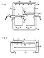
- Figure 1 shows the known circuit in the open state in plan view.
- Figure 2 shows the circuit of Figure 1 in cross section along a section line II (see Figure 1), but in the non-opened state.
- a plastic mass M which can usually be produced by spraying the plastic mass M, serves as the housing.
- a semiconductor chip CH is hermetically enclosed within the housing, ie within the plastic mass M.
- the semiconductor chip CH has pads Pd (generally known as "pads") for contacting the semiconductor chip CH.
- the circuit also contains so-called leads L, which are also used to contact the semiconductor chip CH. They are arranged according to the so-called LOC technology, i.e. above the semiconductor chip CH. Depending on their function, the leads L have several sections (1, 2, 3, P): in a first section 1, a respective lead L is mechanically stably connected to a respective pad Pd (B), for example by means of a wire. Such a connection B is generally referred to as a bond connection.
- the leads L are guided in the second section 2 through the plastic mass M of the integrated circuit to the outside. Outside the integrated circuit, they form connections of the circuit, generally referred to as pins P.
- the third section 3 of a respective lead L is located within the housing of the integrated circuit. It also includes the first section 1 of the respective lead L. It connects to the second section 2.
- a double-sided adhesive film F is provided on that surface of the semiconductor chip CH which has the connection areas Pd, which is arranged between the surface of the semiconductor chip CH and the leads L. It covers practically the entire surface with the exception of those areas in which the pads Pd are arranged. If, as assumed in the integrated circuit according to FIGS. 1, 2, the semiconductor chip CH has connection pads Pd which are arranged along an assumed central axis of the semiconductor chip CH, instead of a single adhesive film F two adhesive films F are arranged next to one another such that the connection pads Pd remain free.
- the adhesive film F essentially serves two purposes: on the one hand, before and during the spraying process, ie before and during the application of the housing, it serves to securely fix the leads L with respect to the semiconductor chip CH, so that in particular no damage to the connections B can occur (for example by unintentionally moving the leads L). On the other hand, it protects the surface of the semiconductor chip CH against damage from the leads L, in particular against damage from scratches. In this circuit ( Figures 1, 2) according to the prior art, the disadvantages and damage described above occur.
- Figures 3 and 4 show a first embodiment of the integrated circuit according to the invention in plan view ( Figure 3) and in cross section ( Figure 4).
- the embodiment according to FIGS. 3, 4 has the same features as the circuit according to FIGS. 1, 2 with the exception of the adhesive film F.
- An adhesive film F according to FIGS. 1, 2, which essentially covers the entire semiconductor chip CH, is in the circuit according to the invention not provided. Instead, an adhesive Adh is applied to each individual lead L between the lead L and the semiconductor chip CH. It is located essentially exclusively between the respective lead L and the semiconductor chip CH, apart from a small amount of excess adhesive Adh that may swell laterally when the leads L are applied.
- Adb calf material so applied is the same as that regarding of the circuit according to Figures 1, 2 already described purpose of the adhesive film F, namely fixing of the leads L before and during the spraying process and protection against damage to the semiconductor chip CH by the leads L.
- those surface areas of the semiconductor chip CH are consequently , which are between the leads L, free of adhesive film F or adhesive Adh.
- adhesive Adh adhesive Adh
- Figures 5 and 6 show a second embodiment of the circuit according to the invention. It largely corresponds to the first embodiment described. However, as in the first embodiment, the adhesive Adh is not arranged in the entire area of the third section 3 of a respective lead L, but rather only in a partial area III of the third section 3. The partial area III in particular comprises the first section 1, as shown in FIG. 6 evident.
- Figures 7 and 8 show a third embodiment of the invention. It is a further development of the second embodiment and differs from it in that the partial area III is essentially point-shaped.
- the section III designed in this way is located below the location of the first section 1 at which the connection B is fastened on the lead L in question.
- FIG. 9 shows a section of one of the third embodiment derived fourth embodiment of the circuit according to the invention. It differs from the third embodiment in that the leads L are cranked at that point of the third section 3 at which the respective section III begins.
- This has the advantage that during the spraying process between the leads L and the surface of the semiconductor chip CH, more plastic mass M can accumulate in the subregions of the third sections 3 remaining outside the subregions III than in the previously described embodiments, because the distances between the leads L and the semiconductor chip CH are correspondingly larger at the relevant points. This leads to greater mechanical stabilization of the leads by the spraying process.
- the first sections 1 each lie in the partial areas III of the third sections 3.
- Figure 10 shows a further advantageous embodiment of the invention.
- At least one of the leads L of the circuit in the third section 3 has a plurality of first sections 1 and a plurality of sub-areas III.
- a respective first section 1 is located in a respective sub-area III.
- the circuit can then be supplied with a supply potential (VDD or VSS) at several locations on the semiconductor chip CH at the same time, with a lower voltage drop due to an ohmic resistance along the relevant leads L than with a supply via a connecting line within the circuit
- FIGS. 3 to 8 and 10 show a further advantageous feature in addition to the features described so far: in this case, on the surface of the semiconductor chip CH having the connection surfaces Pd, edge regions R which run along longitudinal sides R1 of the semiconductor chip CH are free of pads Pd. With this arrangement, it is possible to design electrical circuits, which are contained in the semiconductor chip CH, in terms of their layout such that they extend into these edge regions R. This leads to better utilization of the chip area of the semiconductor chip CH by the electrical circuits contained in the semiconductor chip CH.
Landscapes
- Engineering & Computer Science (AREA)
- Computer Hardware Design (AREA)
- Microelectronics & Electronic Packaging (AREA)
- Power Engineering (AREA)
- Physics & Mathematics (AREA)
- Condensed Matter Physics & Semiconductors (AREA)
- General Physics & Mathematics (AREA)
- Lead Frames For Integrated Circuits (AREA)
Priority Applications (2)
| Application Number | Priority Date | Filing Date | Title |
|---|---|---|---|
| EP92111167A EP0576708A1 (fr) | 1992-07-01 | 1992-07-01 | Circuit intégré avec une grille de conducteurs |
| JP5173812A JPH0685150A (ja) | 1992-07-01 | 1993-06-21 | 集積回路 |
Applications Claiming Priority (1)
| Application Number | Priority Date | Filing Date | Title |
|---|---|---|---|
| EP92111167A EP0576708A1 (fr) | 1992-07-01 | 1992-07-01 | Circuit intégré avec une grille de conducteurs |
Publications (1)
| Publication Number | Publication Date |
|---|---|
| EP0576708A1 true EP0576708A1 (fr) | 1994-01-05 |
Family
ID=8209767
Family Applications (1)
| Application Number | Title | Priority Date | Filing Date |
|---|---|---|---|
| EP92111167A Withdrawn EP0576708A1 (fr) | 1992-07-01 | 1992-07-01 | Circuit intégré avec une grille de conducteurs |
Country Status (2)
| Country | Link |
|---|---|
| EP (1) | EP0576708A1 (fr) |
| JP (1) | JPH0685150A (fr) |
Cited By (4)
| Publication number | Priority date | Publication date | Assignee | Title |
|---|---|---|---|---|
| DE4435115A1 (de) * | 1994-09-30 | 1996-04-04 | Siemens Ag | Verfahren zur Herstellung einer LOC-Anordnung |
| US5684330A (en) * | 1995-08-22 | 1997-11-04 | Samsung Electronics Co., Ltd. | Chip-sized package having metal circuit substrate |
| DE19633712C1 (de) * | 1996-08-21 | 1998-04-16 | Siemens Components | Vorrichtung zum Aufbringen eines Klebebands auf ein Leadframe |
| US5917242A (en) * | 1996-05-20 | 1999-06-29 | Micron Technology, Inc. | Combination of semiconductor interconnect |
Families Citing this family (1)
| Publication number | Priority date | Publication date | Assignee | Title |
|---|---|---|---|---|
| JP3638750B2 (ja) * | 1997-03-25 | 2005-04-13 | 株式会社ルネサステクノロジ | 半導体装置 |
Citations (4)
| Publication number | Priority date | Publication date | Assignee | Title |
|---|---|---|---|---|
| EP0329317A2 (fr) * | 1988-02-12 | 1989-08-23 | Hitachi, Ltd. | Dispositif semi-conducteur comprenant une feuille isolante |
| EP0409173A2 (fr) * | 1989-07-19 | 1991-01-23 | Nec Corporation | Dispositif à circuit intégré semi-conducteur ayant une structure d'interconnexion améliorée |
| US5086018A (en) * | 1991-05-02 | 1992-02-04 | International Business Machines Corporation | Method of making a planarized thin film covered wire bonded semiconductor package |
| EP0478250A1 (fr) * | 1990-09-24 | 1992-04-01 | Texas Instruments Incorporated | Dispositif à circuit intégré et méthode pour éviter les craquelures pendant le montage en surface |
Family Cites Families (4)
| Publication number | Priority date | Publication date | Assignee | Title |
|---|---|---|---|---|
| JPH0327562A (ja) * | 1989-06-23 | 1991-02-05 | Nec Corp | 半導体装置 |
| JP2569939B2 (ja) * | 1989-10-23 | 1997-01-08 | 日本電気株式会社 | 樹脂封止型半導体装置 |
| JPH03235360A (ja) * | 1990-02-09 | 1991-10-21 | Nec Corp | 樹脂封止型半導体装置 |
| JP2983620B2 (ja) * | 1990-07-20 | 1999-11-29 | 株式会社日立製作所 | 半導体装置及びその製造方法 |
-
1992
- 1992-07-01 EP EP92111167A patent/EP0576708A1/fr not_active Withdrawn
-
1993
- 1993-06-21 JP JP5173812A patent/JPH0685150A/ja active Pending
Patent Citations (4)
| Publication number | Priority date | Publication date | Assignee | Title |
|---|---|---|---|---|
| EP0329317A2 (fr) * | 1988-02-12 | 1989-08-23 | Hitachi, Ltd. | Dispositif semi-conducteur comprenant une feuille isolante |
| EP0409173A2 (fr) * | 1989-07-19 | 1991-01-23 | Nec Corporation | Dispositif à circuit intégré semi-conducteur ayant une structure d'interconnexion améliorée |
| EP0478250A1 (fr) * | 1990-09-24 | 1992-04-01 | Texas Instruments Incorporated | Dispositif à circuit intégré et méthode pour éviter les craquelures pendant le montage en surface |
| US5086018A (en) * | 1991-05-02 | 1992-02-04 | International Business Machines Corporation | Method of making a planarized thin film covered wire bonded semiconductor package |
Cited By (6)
| Publication number | Priority date | Publication date | Assignee | Title |
|---|---|---|---|---|
| DE4435115A1 (de) * | 1994-09-30 | 1996-04-04 | Siemens Ag | Verfahren zur Herstellung einer LOC-Anordnung |
| DE4435115C2 (de) * | 1994-09-30 | 1999-01-21 | Siemens Ag | Verfahren zur Herstellung einer Lead-On-Chip (LOC)-Anordnung |
| US5684330A (en) * | 1995-08-22 | 1997-11-04 | Samsung Electronics Co., Ltd. | Chip-sized package having metal circuit substrate |
| US5917242A (en) * | 1996-05-20 | 1999-06-29 | Micron Technology, Inc. | Combination of semiconductor interconnect |
| US6080264A (en) * | 1996-05-20 | 2000-06-27 | Micron Technology, Inc. | Combination of semiconductor interconnect |
| DE19633712C1 (de) * | 1996-08-21 | 1998-04-16 | Siemens Components | Vorrichtung zum Aufbringen eines Klebebands auf ein Leadframe |
Also Published As
| Publication number | Publication date |
|---|---|
| JPH0685150A (ja) | 1994-03-25 |
Similar Documents
| Publication | Publication Date | Title |
|---|---|---|
| EP0299530B1 (fr) | Support pour la fabrication de cartes d'identification | |
| EP0484353B1 (fr) | Element-support presentant au moins un circuit integre, destine notamment a etre monte dans des cartes a puces | |
| EP0682321B1 (fr) | Porteur d'information à puce et procédé de préparation d'un porteur d'information | |
| DE69938582T2 (de) | Halbleiterbauelement, seine herstellung, leiterplatte und elektronischer apparat | |
| DE69839276T2 (de) | Verfahren zum herstellen einer chipkarte, geeignet zum kontaktbehafteten oder kontaktlosen betrieb | |
| DE3814469C2 (fr) | ||
| DE2732529C2 (de) | Gedruckte Schaltungsplatine | |
| DE3616494A1 (de) | Integrierte schaltungspackung und verfahren zur herstellung einer integrierten schaltungspackung | |
| DE10352946A1 (de) | Halbleiterbauteil mit Halbleiterchip und Umverdrahtungslage sowie Verfahren zur Herstellung desselben | |
| DE19755675B4 (de) | Halbleitergehäuse und Verfahren zu dessen Herstellung | |
| DE102006033864A1 (de) | Elektronische Schaltung in einer Package-in-Package-Konfiguration und Herstellungsverfahren für eine solche Schaltung | |
| EP0009610A1 (fr) | Procédé pour la fabrication de conteneurs testables miniaturisés en forme de bande pour semi-conducteurs | |
| EP0576708A1 (fr) | Circuit intégré avec une grille de conducteurs | |
| DE10255289A1 (de) | Elektronisches Bauteil mit gestapelten Halbleiterchips in paralleler Anordnung und Verfahren zu dessen Herstellung | |
| DE3130072A1 (de) | Integriertes schaltglied | |
| EP1065624A2 (fr) | Module puce à monter dans un support de carte à puce | |
| DE19743264C2 (de) | Verfahren zur Herstellung einer Emulationsschaltkreisanordnung sowie Emulationsschaltkreisanordnung mit zwei integrierten Schaltkreisen | |
| DE4130569A1 (de) | Ic-paketiereinrichtung | |
| DE2528119A1 (de) | Elektrisch leitendes band | |
| DE3619636A1 (de) | Gehaeuse fuer integrierte schaltkreise | |
| EP0852774B1 (fr) | Module de puce | |
| DE4113034A1 (de) | System und verfahren zum automatisierten bandbonden, die die reparatur erleichtern | |
| WO1998033211A1 (fr) | Procede de mise sous boitier de circuits de commande integres | |
| DE4425943B4 (de) | Verfahren zur Herstellung eines mehrschichtigen Leiter- bzw. Anschlusselements und Leiter- bzw. Anschlusselement | |
| DE19747177C2 (de) | Gehäustes Bauelement und Verfahren zu dessen Herstellung |
Legal Events
| Date | Code | Title | Description |
|---|---|---|---|
| PUAI | Public reference made under article 153(3) epc to a published international application that has entered the european phase |
Free format text: ORIGINAL CODE: 0009012 |
|
| AK | Designated contracting states |
Kind code of ref document: A1 Designated state(s): AT DE FR GB IT NL |
|
| 17P | Request for examination filed |
Effective date: 19940620 |
|
| 17Q | First examination report despatched |
Effective date: 19960325 |
|
| STAA | Information on the status of an ep patent application or granted ep patent |
Free format text: STATUS: THE APPLICATION IS DEEMED TO BE WITHDRAWN |
|
| 18D | Application deemed to be withdrawn |
Effective date: 19960806 |