EP0571148B1 - Circuit de commande automatique de gain non-linéaire pour utilisation dans une boucle à verrouillage de phase - Google Patents
Circuit de commande automatique de gain non-linéaire pour utilisation dans une boucle à verrouillage de phase Download PDFInfo
- Publication number
- EP0571148B1 EP0571148B1 EP93303771A EP93303771A EP0571148B1 EP 0571148 B1 EP0571148 B1 EP 0571148B1 EP 93303771 A EP93303771 A EP 93303771A EP 93303771 A EP93303771 A EP 93303771A EP 0571148 B1 EP0571148 B1 EP 0571148B1
- Authority
- EP
- European Patent Office
- Prior art keywords
- signal
- circuit
- phase difference
- pll circuit
- output
- Prior art date
- Legal status (The legal status is an assumption and is not a legal conclusion. Google has not performed a legal analysis and makes no representation as to the accuracy of the status listed.)
- Expired - Lifetime
Links
- 238000000034 method Methods 0.000 claims description 18
- 230000001360 synchronised effect Effects 0.000 claims description 4
- 230000003247 decreasing effect Effects 0.000 claims 1
- 230000002401 inhibitory effect Effects 0.000 claims 1
- 238000010586 diagram Methods 0.000 description 2
- 238000005259 measurement Methods 0.000 description 2
- 239000003990 capacitor Substances 0.000 description 1
- 238000010276 construction Methods 0.000 description 1
- 230000001419 dependent effect Effects 0.000 description 1
Images

Classifications
-
- H—ELECTRICITY
- H03—ELECTRONIC CIRCUITRY
- H03L—AUTOMATIC CONTROL, STARTING, SYNCHRONISATION OR STABILISATION OF GENERATORS OF ELECTRONIC OSCILLATIONS OR PULSES
- H03L7/00—Automatic control of frequency or phase; Synchronisation
- H03L7/06—Automatic control of frequency or phase; Synchronisation using a reference signal applied to a frequency- or phase-locked loop
- H03L7/08—Details of the phase-locked loop
- H03L7/085—Details of the phase-locked loop concerning mainly the frequency- or phase-detection arrangement including the filtering or amplification of its output signal
- H03L7/089—Details of the phase-locked loop concerning mainly the frequency- or phase-detection arrangement including the filtering or amplification of its output signal the phase or frequency detector generating up-down pulses
-
- H—ELECTRICITY
- H03—ELECTRONIC CIRCUITRY
- H03L—AUTOMATIC CONTROL, STARTING, SYNCHRONISATION OR STABILISATION OF GENERATORS OF ELECTRONIC OSCILLATIONS OR PULSES
- H03L7/00—Automatic control of frequency or phase; Synchronisation
- H03L7/06—Automatic control of frequency or phase; Synchronisation using a reference signal applied to a frequency- or phase-locked loop
- H03L7/08—Details of the phase-locked loop
- H03L7/10—Details of the phase-locked loop for assuring initial synchronisation or for broadening the capture range
- H03L7/107—Details of the phase-locked loop for assuring initial synchronisation or for broadening the capture range using a variable transfer function for the loop, e.g. low pass filter having a variable bandwidth
- H03L7/1077—Details of the phase-locked loop for assuring initial synchronisation or for broadening the capture range using a variable transfer function for the loop, e.g. low pass filter having a variable bandwidth by changing characteristics of the phase or frequency detection means
Definitions
- This invention relates to improvements in phase-locked loop circuitry and methods for operating same, and to improvements in circuitry and methods for reducing steady state error and increasing the capture range of a PLL during convergence by automatically changing the gain applied to the signal from the phase detector.
- variable frequency circuit can be a voltage-controlled oscillator (VCO), but in the embodiment illustrated herein, the variable frequency circuit includes a variable speed motor and a generator that produces a signal of frequency dependent upon the speed of the motor.
- the phase of the variable frequency signal with respect to the reference frequency is determined by the phase detector, and the phase detector generates a dc voltage signal, which may be filtered by the integrating filter, to control the variable frequency signal, for example, by controlling the frequency of a VCO or by controlling the speed of the motor.
- the voltage signal forces the VCO to compensate, or changes the speed of the motor, when the variable frequency drifts from the reference frequency.
- variable frequency typically requires a certain time to converge to the frequency of the input signal, until "lock" occurs.
- lock occurs, the variable frequency tracks the input signal, and the PLL circuit functions in a feedback mode to maintain the lock.
- a higher gain applied to the signal from the phase detector reduces the steady state operation error.
- a low gain applied to the phase detector output signal widens the lock, or capture, range.
- What is needed is a circuit and method that will provide a lower gain when the phase error between the reference frequency and the variable frequency is large, during convergence, and a higher gain when the phase error is low, when lock has been, or is close to being, attained.
- the circuit and method should provide multiple break points (changes in the gain) in the transfer function if desired, so that a smooth and approximately linear change of phase detector output voltage is obtainable, and the PLL performance can be maximized.
- DE-A-3 743 158 discloses a PLL circuit for generating signals to control a motor speed, in which a signal is generated having a frequency proportional to the speed of the motor.
- a PLL circuit for generating drive signals to control the speed of a motor according to a reference frequency, comprising:
- a method for generating a drive signal to a motor comprising:
- the invention thus provides a PLL circuit for generating drive signals to control the speed of a motor according to a reference frequency.
- a motor speed circuit generates a speed signal of frequency proportional to the speed of the motor, and a phase detector produces a signal of duration proportional to a phase difference between the speed signal and the reference frequency signal.
- a phase difference measuring circuit produces a first output signal at a first gain proportional to the phase difference when the duration of the phase detector signal is less than a predetermined time and produces a second output signal at a second gain less than the first gain when the duration of the phase detector signal is greater than the predetermined time.
- the first and second output signals are summed to produce a summed signal that is applied to a motor driver circuit for controlling the speed of the motor.
- the present invention further provides a PLL circuit which controls a variable frequency signal to be synchronized to a reference frequency signal.
- the circuit includes a circuit to generate a speed signal proportional to the speed of the motor.
- a phase detector produces a signal for a duration proportional to the phase difference between the speed signals and the reference frequency signal.
- a first phase difference measuring circuit produces a first output signal at a first gain proportional to the phase difference when the duration of the phase detector signal is less than a predetermined time
- a second phase difference measuring circuit produces a second output signal at a second gain when the duration of the phase detector signal is greater than the predetermined time.
- the first and second output signals are summed for application to control the speed of the motor.
- the first gain is larger than the second gain, the difference due to clocks at first and second frequencies to clock first and second digital counters.
- the second digital counter is enabled only when the first counter saturates, so that the first counter controls the operation of the circuit at and near lock, and the second controls the operation of the circuit during convergence toward the lock range.
- a first control signal is generated at a first gain.
- the first control signal operates within a first range of phase difference between the resultant signal and a reference signal.
- a second control signal is generated at a second gain lower than the first gain.
- the second control signal operates within a second range of phase difference between the resultant signal and a reference signal larger than the first range of phase difference.
- the first and second control signals are summed, and the drive signals are modified according to the summed first and second control signals.
- Figure 1 is an electrical schematic diagram of a PLL circuit with non-linear gain according to a preferred embodiment of the invention for driving a motor that can be connected to the PLL circuit.
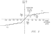
- Figure 2 is a graph of the output voltage of the phase detector circuit as a function of the phase difference between the reference frequency and a motor speed signal.
- An electrical schematic diagram of a PLL circuit 10 incorporates an automatic gain control (AGC) circuit 41 with non-linear gain according to a preferred embodiment of the invention, as shown in Figure 1.
- AGC automatic gain control
- the PLL circuit 10 can be constructed of discrete components, preferably all or portions of it can be integrated onto a single integrated-circuit device. Also, although the circuit has particular application with motor driving circuits, it is to be appreciated that the PLL circuit 10 may find application in many other types of circuits.
- the AGC circuit 41 serves to create an analog voltage at a low gain to the input of a motor driving circuit 100 during the initial circuit startup mode, or if an event occurs that causes the PLL to lose lock. In such instances, a motor speed signal on line 12 to be tracked by the PLL circuit and the reference frequency on line 14 are of greatly differing frequencies.
- the motor speed signal can be, for instance, a signal of spaced pulses based upon rotor position representing the speed of rotation of the rotor.
- the AGC circuit 41 also serves to create a voltage at a high gain to the input of the motor driver circuitry 100 once a lock range has been reached by the PLL circuit 10, or the phase error is relatively small.
- the PLL circuit 10 uses a phase detector 11 that includes a frequency/phase detector 16, a pair of up-down counters 30 and 44, a pair of latches 52 and 56, a pair of digital to analog converters 60 and 62, for providing the non-linear gain that is necessary to obtain the desired PLL performance, and a summing amplifier 69 to provide a signal to be applied to the motor driver circuitry 100.
- a phase detector 11 that includes a frequency/phase detector 16, a pair of up-down counters 30 and 44, a pair of latches 52 and 56, a pair of digital to analog converters 60 and 62, for providing the non-linear gain that is necessary to obtain the desired PLL performance, and a summing amplifier 69 to provide a signal to be applied to the motor driver circuitry 100.
- the motor speed signal is applied on line 12 to one input of the frequency/phase detector 16, and the reference frequency is applied on another line 14 to another input.
- the frequency/phase detector 16 operates to detect a phase difference between the two signals, and may be, for example a commercially available phase detector, such as an MC4044 phase/frequency detector circuit.
- the frequency/phase detector 16 has two outputs on lines 20 and 22.
- the output on the line 20 indicates that the reference frequency on line 14 leads the phase motor speed signal on line 12, indicating that the motor speed is less than the desired speed, and needs to be increased.
- the output on the line 22 indicates that the phase motor speed signal on line 12 leads the reference frequency on line 14, indicating that the motor speed exceeds the desired speed, and needs to be slowed.
- the frequency/phase detector 16 determines the time difference between the occurrence of the incoming pulse edges of the motor speed signal on line 12 and the reference frequency on line 14.
- the output on either line 20 or 22 from the frequency/phase detector 16 is a pulse of length equal or proportional to the time difference between the active edges of the pulses on lines 12 and 14 to control the counters 30 and 44 to count either up or down for that time.
- the frequency/phase detector 16 detects the falling edge of a motor speed signal pulse on line 12 before it detects a falling edge of the reference frequency on line 14, it will emit a pulse on the "down" line 22 to control the counters 30 and 44 to count down.
- the frequency/phase detector 16 If the falling edge of the reference frequency on line 14 arrives before the falling edge of the motor speed signal pulse on line 12, the frequency/phase detector 16 emits a pulse on the "up" line 20. As noted, the length of the frequency/phase detector 16 output pulse in any event is equal or proportional to the phase difference of the incoming signals.
- Two counters 30 and 44 are connected to receive the up and down signal pulses from the frequency/phase detector 16 on lines 20 and 22.
- the counter 44 serves as a "fine” counter, and receives clock signals from a clock 23 at a high frequency, for example 2 mHz, on line 42.
- the output from the "fine” counter 44 appears on a plurality of output lines 40-40, which may be, for example, an 8 bit wide bus.
- the outputs from the "fine" counter 44 on lines 40-40 are applied to an over- and underflow detector circuit 24 to produce an output signal on a line 28 to the upper counter 30, in a manner below described, in the event an over- or underflow occurs in the count of the "fine" counter 44.
- the function of the counters 30 and 44 can be performed by other types of counters, for instance, counters that have a single input for counting either up or down depending on the sign of the pulse emitted from the phase detector.
- a qualifying gate pulse also may be provided to gate the clock in such embodiment.
- the upper counter 30 serves as a "coarse” counter, and receives clock signals on an input line 36 from an AND gate 34.
- the clock signals provided by the AND gate 34 represent the logical combination of a low frequency clock signal, for example, 15.6 kHz, from a low frequency clock 25 on the line 32, and the output signal from the over-underflow detector 24.
- the 15.6 kHz clock signal is inhibited from clocking the "coarse” counter 30, unless the under- or overflow signal also appears on the line 28.
- the output from the "coarse” counter 30 appears on output lines 38-38, which may also be an 8 bit bus.
- the counters 30 and 44 When the counters 30 and 44 are reset, both initialize to count up or down from an intermediate count value centered between their over- and underflow states. Thus, for example, if the counters are 8-bit counters, when they are reset, they initialize to the count 10000000, from which either an up or down count can be made. Additionally, the counters are of the type that stop counting when an overflow or underflow condition occurs to hold at the over- or underflow count, instead of continuing to count, or wrapping around. The counters are reset after the termination of the counting period generated by either signal on line 20 or line 22. The termination of such signal is detected in an edge detector circuit 25. The edge detector circuit 25 generates "latch" signals on lines 48 and 47 to store the value in the counters 44 and 30 and reset them.
- the "fine" counter 44 counts while a pulse on one of the lines 20 or 22 exists.
- the direction of the count of the counter 44 depends on which of line 20 or 22 the pulse from the frequency/phase detector 16 exists.
- the count of clock pulses appears on the output lines 40-40.
- the "coarse” counter 30 counts up or down depending on which of lines 20 or 22 the phase difference pulse from the frequency/phase detector 16 appears.
- the AND gate 34 blocks the clock pulses, unless the output from the over- and underflow detector 24 indicates the "fine" counter 44 has reached saturation at an over- or underflow condition.
- the "coarse" counter 30 When such over- or underflow condition occurs, the "coarse" counter 30 counts clock pulses from the low frequency clock generator 25 on line 32 during the duration of the difference pulse on line 20 or 22. The output count from the "coarse” counter 30 appears on output lines 38-38.
- Data latches 52 and 56 receive the data carried on lines 38-38 and 40-40 on their respective inputs.
- the latch function of each latch 52 and 56 is enabled by a signal on the latch line 48 from the edge detector circuit 25, indicating completion of the phase difference measurement.
- the data outputs from the respective "fine” and “coarse” counters 44 and 30 are latched into the respective latches 56 and 52.
- the time in which the phase difference measurement is completed is, for example, when the falling edge of the last occurring pulse of the motor speed signal or the reference frequency occurs, as determined by the edge detector circuit 25.
- the output of the latch 52 developed upon lines 54-54 is applied to a "coarse” digital to analog converter circuit 60.
- the output from the latch 56 developed on lines 58-58 is applied to the input of a "fine” digital to analog converter circuit 62.
- the outputs from the respective "coarse” and “fine” digital to analog converters 60 and 62 are connected to resistors 64 and 66 to be summed on a summing node 63.
- the values of resistors 64 and 66 can be chosen to weight the relative values of the digital to analog converters 60 and 62, in a manner below described.
- the resistors 64 and 66 serve as input resistors to the inverting input 70 of a summing amplifier circuit 69 that includes an operational amplifier 68 having a resistor 76 connected to an analog ground 75 from its non-inverting input terminal 74, and a feedback resistor 72 connected between its output and the inverting input 70.
- the summing amplifier circuit 69 is biased by the resistor 76 so that the voltage applied to the inverting input 70 by the "coarse” and "fine” digital to analog converters 60 and 62 is equal to the voltage on the analog ground 75 when the digital to analog converters 60 and 62 are driven by the "reset” value (eg., 10000000).
- the values of the resistors 64, 66 and 72 of the summing amplifier circuit 69 are selected, as indicated above, to provide desired weights to the output signals of the digital to analog converters 60 and 62.
- the resistor 72 can be provided with a value, R. If the value of resistor 64 is also of value R, the maximum value of the signal at the output node 71 of the amplifier 68 due to the contribution of the digital to analog converter 60 would be the maximum value of the signal at the output of the digital to analog converter 60 times the closed loop gain (-1) of the amplifier 68.
- the value of the resistor 66 is, for example, 16R, then the contribution of output voltage seen at the output node 71 from a maximum value of the output of the "fine” digital to analog converter 62 would be -1/16 the maximum value due to the contribution from the "coarse" digital to analog converter 60.
- the resulting output seen at the output node 71 therefore would be as shown in Figure 2.
- the slope of the curve in the portion 110 near lock, or close to zero phase difference, is significantly larger than the slope of the lines 111 and 112 as the phase difference increases, away from the lock range.
- the voltage output from the summing amplifier circuit 69 on the output node 71 is applied to a filter circuit 80 and an integrator circuit 89 for application to the motor driver circuit 100.
- the integrator circuit 89 is of known construction, having an operational amplifier 86 and a resistor 94 connected between the non-inverting input terminal 92 and the analog ground 75.
- the output node 85 of the operational amplifier 86 is connected to the inverting input terminal 84 by a capacitor 90 and resistor 88, connected in series.
- the output from the power driver circuit 100 is connected to the motor 102 to control its rotation.
- a motor condition indicating signal on line 12 representing, for example, the speed of rotation of the motor, is connected to another input of the frequency/phase detector 16.
- the "fine" counter 44 no longer saturates between reset pulses and the over- underflow detector circuit 24 no longer enables the AND gate 34 to pass the 15.6 kHz clock signal. In this lock mode, therefore, the "coarse" counter 30 is disabled.
- the "fine" counter 44 with its associated “fine” digital to analog converter 62 generates an output voltage on the resistor 66 that has a high gain, since the number of 2 mHz clock pulses 42 occurring during a phase error period will be relatively large, causing a large voltage gain out of the "fine” digital to analog converter 62. Also, the output of the "coarse” counter 30 and “coarse” digital to analog converter 60 will have a low voltage gain, since the "coarse” counter 30 counts a relatively lower number of pulses from the 15.6 kHz clock during a phase error period, and therefore the digital to analog converter 60 will output an analog voltage with a much lower gain relative to the phase error to the resistor 64.
- Figure 2 depicts the output voltage of the AGC circuit 41 at the output node 71 as a function of the phase difference between the motor speed signal and the reference frequency.
- This graph shows that if the difference between the edges of the two pulses is less than 64 microseconds, only the "fine" counter 44 can count.
- the voltage on the output node 71 is steep from -64 to +64 microseconds.
- +64 microseconds might, for example, indicate the motor speed signal has its falling edge +64 microseconds after of a falling edge of the reference signal. In that case, the -64 microsecond time would indicate that the falling edge of the reference frequency occurs 64 microseconds after of the falling edge of the motor speed signal.
- This is "high-gain" in the sense that the output signal rises rapidly as a function of time.
- the "fine” counter 44 reaches saturation to enable the "coarse” counter 30. Beyond that point the "staircase” graphs 111 and 112 appear because the gain of the "coarse” counter 30 through the summing amplifier 69 is much larger than the gain of the "fine” counter 44. On the other hand, the time for each step of the "fine” counter 44 is very small, resulting in the straight line appearance of the segment 110 in the scale illustrated. Because the "fine” counter 44 has 256 steps between the -64 microseconds and +64 microseconds times in the graph, the horizontal length per step is also small.
- the idea embodied by the AGC circuitry 41 for creating a non-linear gain for the PLL circuit 10 may be extended to create multiple break points in the transfer function (i.e., multiple gain-changes occurring at different points in the operation) by adding more gain paths in parallel.
Landscapes
- Control Of Electric Motors In General (AREA)
Claims (22)
- Circuit de boucle à verrouillage de phase (10) pour produire des signaux de commande pour commander la vitesse d'un moteur (102) en fonction d'une fréquence de référence (FREF), comprenant :
un circuit pour produire un signal de vitesse (12) de fréquence proportionnelle à la vitesse du moteur (102),
caractérisé en ce que le circuit de boucle à verrouillage de phase (10) comprend en outre :un détecteur de phase (16) pour fournir un signal de durée proportionnelle à une différence de phase entre le signal de vitesse (12) et le signal de fréquence de référence (FREF) ;un circuit de mesure de différence de phase (44, 30) pour délivrer un premier signal de sortie avec un premier gain proportionnel à la différence de phase lorsque la durée du signal du détecteur de phase susmentionné (20, 22) est inférieure à une durée prédéterminée et pour délivrer un deuxième signal de sortie avec un deuxième gain inférieur au premier gain lorsque la durée du signal du détecteur de phase susmentionné (20, 22) est supérieure à la durée prédéterminée susmentionnée ; etun noeud (63) au niveau duquel les premier et deuxième signaux de sortie sont additionnés pour produire un signal somme (71) pour commander la vitesse du moteur (102). - Circuit de boucle à verrouillage de phase (10) selon la revendication 1, dans lequel le circuit de mesure de différence de phase (44, 30) comprend un premier circuit de mesure de différence de phase (44) pour délivrer le premier signal de sortie et un deuxième circuit de mesure de différence de phase (30) pour délivrer le deuxième signal de sortie.
- Circuit de boucle à verrouillage de phase (10) selon la revendication 1 ou la revendication 2, comprenant en outre un circuit de commande de moteur (100), dans lequel le signal somme susmentionné est appliqué au circuit de commande de moteur (100).
- Circuit de boucle à verrouillage de phase (10) selon l'une quelconque des revendications 1 à 3, comprenant en outre des moyens (64, 66) de pondération des premier et deuxième signaux de sortie avant que les premier et deuxième signaux de sortie ne soient additionnés.
- Circuit de boucle à verrouillage de phase (10) selon l'une quelconque des revendications 1 à 4, dans lequel le premier gain est plus grand que le deuxième gain.
- Circuit de boucle à verrouillage de phase (10) selon l'une quelconque des revendications 1 à 5, dans lequel le circuit de mesure de différence de phase (44, 30) est un circuit numérique.
- Circuit de boucle à verrouillage de phase (10) selon la revendication 6, dans lequel le circuit de mesure de différence de phase (44, 30) comprend des compteurs (30, 44).
- Circuit de boucle à verrouillage de phase (10) selon l'une quelconque des revendications 2 à 7, dans lequel les premier (44) et deuxième (30) circuits de mesure de différence de phase sont un premier (30) et un deuxième (44) compteur.
- Circuit de boucle à verrouillage de phase (10) selon la revendication 7, dans lequel les compteurs (44, 30) sont un premier (44) et un deuxième (30) compteur/décompteur.
- Circuit de boucle à verrouillage de phase (10) selon la revendication 9, dans lequel les premier (44) et deuxième (30) compteurs/décompteurs sont initialisés à une valeur à mi-chemin entre la valeur maximum et la valeur minimum des compteurs (44, 30) susmentionnés.
- Circuit de boucle à verrouillage de phase (10) selon la revendication 4, dans lequel les moyens de pondération (66, 64) des premier et deuxième signaux de sortie sont respectivement une première (66) et une deuxième (64) résistance.
- Circuit de boucle à verrouillage de phase (10) selon la revendication 10, dans lequel les première (66) et deuxième (64) résistances sont de taille telle que la pondération du deuxième signal de sortie soit 16 fois la pondération du premier signal de sortie.
- Circuit de boucle à verrouillage de phase (10) selon l'une quelconque des revendications 7 à 12, comprenant en outre un premier (23) et un deuxième (25) générateur pour produire un premier (42) et un deuxième (32) signal d'horloge pour séquencer respectivement les premier (44) et deuxième (30) compteurs.
- Circuit de boucle à verrouillage de phase (10) selon la revendication 13, comprenant en outre un circuit d'inhibition (24, 34) pour empêcher le deuxième signal d'horloge (32) de séquencer le deuxième compteur (30) jusqu'à ce que le premier compteur (44) ait compté pendant la durée prédéterminée susmentionnée.
- Circuit de boucle à verrouillage de phase (10) selon la revendication 14, dans lequel le deuxième signal d'horloge (32) a une période égale à la durée prédéterminée susmentionnée.
- Circuit de boucle à verrouillage de phase (10) selon l'une quelconque des revendications 1 à 15, comprenant en outre un filtre intégrateur (89) entre les premier et deuxième signaux de sortie additionnés et le moteur (102).
- Circuit de boucle à verrouillage de phase (10) selon la revendication 2, dans lequel la sortie du détecteur de phase (16) est un signal en impulsion (20, 22) et le deuxième circuit de mesure de différence de phase (30) comprend :et dans lequel le circuit de mesure de différence de phase susmentionné (44) comprend :plusieurs compteurs (30), chacun pour compter des impulsions d'horloge pendant les durées respectives du signal de sortie (20, 22) du détecteur de phase ; etplusieurs générateurs de signal d'horloge (25) pour séquencer l'un respectif desdits compteurs (30) chacun des générateurs de signal d'horloge (25) produisant un signal d'horloge (32) de fréquence proportionnelle au gain de sortie d'un circuit de compteur désiré ;un compteur (44) fonctionnant durant une plus petite durée du signal d'impulsion de sortie du détecteur de phase (20, 22),dans lequel les compteurs (30) du deuxième circuit de mesure de différence de phase (30) sont connectés pour compter seulement après saturation du compteur (44) du premier circuit de mesure de différence de phase (44), lesdits signaux d'horloge (32), appliqués respectivement à chaque compteur (30) du deuxième circuit de mesure de différence de phase (30) qui fonctionne durant une plus grande durée, étant de fréquences décroissantes, ce qui entraíne qu'un transfert de gain discontinu est obtenu.
- Circuit de boucle à verrouillage de phase (10) selon la revendication 17, dans lequel les compteurs (30, 44) sont des compteurs numériques, et comprennent en outre un circuit (60, 62) pour convertir des nombres binaires produits par les circuits de comptage numériques en tensions de sortie analogiques.
- Procédé de génération d'un signal de commande (71) pour commander un moteur, comprenant les étapes consistant à produire un signal de vitesse (12) proportionnel à la vitesse d'un moteur (102),
caractérisé en ce qu'il comprend en outre les étapes suivantes :produire une impulsion (20, 22) de longueur proportionnelle à la différence de phase entre le signal de référence (FREF) et un signal de vitesse (12), déterminée par ledit signal de commande et à laquelle le signal de commande doit être synchronisé ;produire un premier signal de commande de tension (58) avec un premier gain, le premier signal de commande de tension (58) étant activé dans une première plage de différence de phase entre le signal résultant (16) et un signal de référence (FREF) ;produire un deuxième signal de commande de tension (54) avec un deuxième gain inférieur au premier gain, le deuxième signal de commande de tension (54) étant activé dans une deuxième plage de différence de phase entre le signal résultant (16) et un signal de référence (FREF) plus grande que la première plage de différence de phase ;additionner les premier (58) et deuxième (54) signaux de commande de tension ; etmodifier le signal de commande (71) en fonction des premier (58) et deuxième (54) signaux de commande de tension additionnés. - Procédé selon la revendication 19, comprenant en outre l'étape consistant à pondérer les premier (58) et deuxième (54) signaux de commande de tension avant l'étape susmentionnée d'addition.
- Procédé selon la revendication 20, dans lequel les étapes consistant à produire les premier (58) et deuxième (54) signaux de commande de tension comprennent le comptage d'une première (42) et d'une deuxième (32) impulsions d'horloge de fréquence différente (23, 25), et la génération d'un premier (58) et d'un deuxième (54) signal de commande de tension à partir des comptages respectifs (40, 38).
- Procédé selon la revendication 22, comprenant en outre l'inhibition du comptage des deuxièmes impulsions d'horloge (32) jusqu'à ce qu'un comptage prédéterminé soit atteint en comptant les premières impulsions d'horloge susmentionnées (42).
Applications Claiming Priority (2)
| Application Number | Priority Date | Filing Date | Title |
|---|---|---|---|
| US07/885,489 US5329560A (en) | 1992-05-19 | 1992-05-19 | AGC circuit with non-linear gain for use in PLL circuit |
| US885489 | 1992-05-19 |
Publications (2)
| Publication Number | Publication Date |
|---|---|
| EP0571148A1 EP0571148A1 (fr) | 1993-11-24 |
| EP0571148B1 true EP0571148B1 (fr) | 1998-04-15 |
Family
ID=25387016
Family Applications (1)
| Application Number | Title | Priority Date | Filing Date |
|---|---|---|---|
| EP93303771A Expired - Lifetime EP0571148B1 (fr) | 1992-05-19 | 1993-05-17 | Circuit de commande automatique de gain non-linéaire pour utilisation dans une boucle à verrouillage de phase |
Country Status (4)
| Country | Link |
|---|---|
| US (1) | US5329560A (fr) |
| EP (1) | EP0571148B1 (fr) |
| JP (1) | JP3304166B2 (fr) |
| DE (1) | DE69317934T2 (fr) |
Families Citing this family (10)
| Publication number | Priority date | Publication date | Assignee | Title |
|---|---|---|---|---|
| US4879600A (en) * | 1987-03-27 | 1989-11-07 | Canon Kabushiki Kaisha | Image sensing apparatus with control for varying the readout methodology |
| US5293445A (en) * | 1992-05-29 | 1994-03-08 | Sgs-Thomson Microelecetronics, Inc. | AGC with non-linear gain for PLL circuits |
| US5661425A (en) * | 1994-06-20 | 1997-08-26 | Sharp Kabushiki Kaisha | Digital PLL circuit |
| US5469478A (en) * | 1994-07-15 | 1995-11-21 | National Semiconductor Corporation | Digital phase lock loop for jitter filtering and frequency offset compensation |
| US5572099A (en) * | 1994-09-30 | 1996-11-05 | Sgs-Thomson Microelectronics, Inc. | Motor speed control with current limit |
| US5543697A (en) * | 1994-10-27 | 1996-08-06 | Sgs-Thomson Microelectronics, Inc. | Circuit and method for controlling the speed of a motor |
| US5689162A (en) * | 1995-06-07 | 1997-11-18 | Sgs-Thomson Microelectronics, Inc. | Apparatus and method for current sensing for motor driver in pwm mode |
| US5723963A (en) * | 1995-06-07 | 1998-03-03 | Sgs-Thomson Microelectronics, Inc. | Apparatus and method for controlling transition between PWM and linear operation of a motor |
| WO2007086502A1 (fr) * | 2006-01-26 | 2007-08-02 | Nihon Dempa Kogyo Co., Ltd. | Circuit d'attaque d'oscillateur vco et synthétiseur de fréquence |
| JP5284517B1 (ja) * | 2012-06-07 | 2013-09-11 | 株式会社東芝 | 測定装置およびプログラム |
Family Cites Families (5)
| Publication number | Priority date | Publication date | Assignee | Title |
|---|---|---|---|---|
| FR2538656B1 (fr) * | 1982-12-23 | 1985-06-07 | Thomson Csf | Procede et circuit d'asservissement en frequence et en phase d'un oscillateur local en television |
| JPS6315530A (ja) * | 1986-07-08 | 1988-01-22 | Sumitomo Electric Ind Ltd | デイジタル位相同期ル−プ |
| US4694259A (en) * | 1986-09-29 | 1987-09-15 | Laser Magnetic Storage International Company | Data tracking clock recovery system having media speed variation compensation |
| JP2724142B2 (ja) * | 1986-12-19 | 1998-03-09 | 株式会社リコー | 回転速度信号発生装置 |
| US5086261A (en) * | 1989-10-31 | 1992-02-04 | Konica Corporation | Motor speed control device for use in an image forming apparatus |
-
1992
- 1992-05-19 US US07/885,489 patent/US5329560A/en not_active Expired - Lifetime
-
1993
- 1993-05-17 EP EP93303771A patent/EP0571148B1/fr not_active Expired - Lifetime
- 1993-05-17 DE DE69317934T patent/DE69317934T2/de not_active Expired - Fee Related
- 1993-05-19 JP JP11701293A patent/JP3304166B2/ja not_active Expired - Fee Related
Also Published As
| Publication number | Publication date |
|---|---|
| DE69317934T2 (de) | 1998-08-27 |
| EP0571148A1 (fr) | 1993-11-24 |
| JPH0654574A (ja) | 1994-02-25 |
| JP3304166B2 (ja) | 2002-07-22 |
| US5329560A (en) | 1994-07-12 |
| DE69317934D1 (de) | 1998-05-20 |
Similar Documents
| Publication | Publication Date | Title |
|---|---|---|
| US7177611B2 (en) | Hybrid control of phase locked loops | |
| US5180993A (en) | Method and arrangement for frequency synthesis | |
| US4587496A (en) | Fast acquisition phase-lock loop | |
| US6816019B2 (en) | Automatically calibrated phase locked loop system and associated methods | |
| EP0085615B1 (fr) | Circuit pour boucle d'asservissement de phase | |
| JPS58186245A (ja) | クロツク回復装置 | |
| KR100326907B1 (ko) | 2개의 귀환루프를 갖는 클럭 승산기 | |
| US5349309A (en) | Second order phase locked loop | |
| EP0571148B1 (fr) | Circuit de commande automatique de gain non-linéaire pour utilisation dans une boucle à verrouillage de phase | |
| US7482880B2 (en) | Frequency modulated output clock from a digital frequency/phase locked loop | |
| AU706217B2 (en) | A loop filter of a phase-locked loop | |
| EP0195500B1 (fr) | Circuit charge-décharge pour boucle d'asservissement de phase | |
| EP0244665A2 (fr) | Appareil et méthode de mesure de l'erreur de détection de données | |
| US5343167A (en) | One-shot control circuit for tracking a voltage-controlled oscillator | |
| EP1458099B1 (fr) | Boucle à verouillage de phase avec conditionement du courant de contrôle par capacité commutée | |
| US6703878B2 (en) | Input jitter attenuation in a phase-locked loop | |
| EP0572161B1 (fr) | CÔntrole automatique et non-linéaire du gain pour circuits à boucle à verrouillage de phase | |
| EP1241790B1 (fr) | Boucle à verrouillage de phase entièrement numérique et circuiterie l'utilisant | |
| JP2885662B2 (ja) | Pll回路 | |
| JPS648541B2 (fr) | ||
| JPH0241026A (ja) | Pll回路 | |
| JP3070076B2 (ja) | 位相同期発振回路 | |
| US6310927B1 (en) | First order tuning circuit for a phase-locked loop | |
| JPH0461421A (ja) | Pll回路 | |
| JP3198687B2 (ja) | Pll回路 |
Legal Events
| Date | Code | Title | Description |
|---|---|---|---|
| PUAI | Public reference made under article 153(3) epc to a published international application that has entered the european phase |
Free format text: ORIGINAL CODE: 0009012 |
|
| AK | Designated contracting states |
Kind code of ref document: A1 Designated state(s): DE FR GB IT |
|
| 17P | Request for examination filed |
Effective date: 19940523 |
|
| 17Q | First examination report despatched |
Effective date: 19961007 |
|
| GRAG | Despatch of communication of intention to grant |
Free format text: ORIGINAL CODE: EPIDOS AGRA |
|
| GRAG | Despatch of communication of intention to grant |
Free format text: ORIGINAL CODE: EPIDOS AGRA |
|
| GRAH | Despatch of communication of intention to grant a patent |
Free format text: ORIGINAL CODE: EPIDOS IGRA |
|
| GRAH | Despatch of communication of intention to grant a patent |
Free format text: ORIGINAL CODE: EPIDOS IGRA |
|
| GRAA | (expected) grant |
Free format text: ORIGINAL CODE: 0009210 |
|
| AK | Designated contracting states |
Kind code of ref document: B1 Designated state(s): DE FR GB IT |
|
| REF | Corresponds to: |
Ref document number: 69317934 Country of ref document: DE Date of ref document: 19980520 |
|
| ITF | It: translation for a ep patent filed |
Owner name: PORTA CHECCACCI E BOTTI S.R.L. |
|
| ET | Fr: translation filed | ||
| PLBE | No opposition filed within time limit |
Free format text: ORIGINAL CODE: 0009261 |
|
| STAA | Information on the status of an ep patent application or granted ep patent |
Free format text: STATUS: NO OPPOSITION FILED WITHIN TIME LIMIT |
|
| RAP4 | Party data changed (patent owner data changed or rights of a patent transferred) |
Owner name: STMICROELECTRONICS, INC. |
|
| 26N | No opposition filed | ||
| REG | Reference to a national code |
Ref country code: GB Ref legal event code: IF02 |
|
| PGFP | Annual fee paid to national office [announced via postgrant information from national office to epo] |
Ref country code: DE Payment date: 20030529 Year of fee payment: 11 |
|
| PGFP | Annual fee paid to national office [announced via postgrant information from national office to epo] |
Ref country code: FR Payment date: 20040510 Year of fee payment: 12 |
|
| PGFP | Annual fee paid to national office [announced via postgrant information from national office to epo] |
Ref country code: GB Payment date: 20040512 Year of fee payment: 12 |
|
| PG25 | Lapsed in a contracting state [announced via postgrant information from national office to epo] |
Ref country code: DE Free format text: LAPSE BECAUSE OF NON-PAYMENT OF DUE FEES Effective date: 20041201 |
|
| PG25 | Lapsed in a contracting state [announced via postgrant information from national office to epo] |
Ref country code: IT Free format text: LAPSE BECAUSE OF NON-PAYMENT OF DUE FEES;WARNING: LAPSES OF ITALIAN PATENTS WITH EFFECTIVE DATE BEFORE 2007 MAY HAVE OCCURRED AT ANY TIME BEFORE 2007. THE CORRECT EFFECTIVE DATE MAY BE DIFFERENT FROM THE ONE RECORDED. Effective date: 20050517 Ref country code: GB Free format text: LAPSE BECAUSE OF NON-PAYMENT OF DUE FEES Effective date: 20050517 |
|
| GBPC | Gb: european patent ceased through non-payment of renewal fee |
Effective date: 20050517 |
|
| PG25 | Lapsed in a contracting state [announced via postgrant information from national office to epo] |
Ref country code: FR Free format text: LAPSE BECAUSE OF NON-PAYMENT OF DUE FEES Effective date: 20060131 |
|
| REG | Reference to a national code |
Ref country code: FR Ref legal event code: ST Effective date: 20060131 |