EP0572161B1 - CÔntrole automatique et non-linéaire du gain pour circuits à boucle à verrouillage de phase - Google Patents
CÔntrole automatique et non-linéaire du gain pour circuits à boucle à verrouillage de phase Download PDFInfo
- Publication number
- EP0572161B1 EP0572161B1 EP93303873A EP93303873A EP0572161B1 EP 0572161 B1 EP0572161 B1 EP 0572161B1 EP 93303873 A EP93303873 A EP 93303873A EP 93303873 A EP93303873 A EP 93303873A EP 0572161 B1 EP0572161 B1 EP 0572161B1
- Authority
- EP
- European Patent Office
- Prior art keywords
- frequency
- circuit
- signal
- counter
- output
- Prior art date
- Legal status (The legal status is an assumption and is not a legal conclusion. Google has not performed a legal analysis and makes no representation as to the accuracy of the status listed.)
- Expired - Lifetime
Links
- 238000000034 method Methods 0.000 claims description 13
- 238000010586 diagram Methods 0.000 description 5
- 238000001514 detection method Methods 0.000 description 2
- 238000005259 measurement Methods 0.000 description 2
- 229920006395 saturated elastomer Polymers 0.000 description 2
- 239000003990 capacitor Substances 0.000 description 1
- 238000010276 construction Methods 0.000 description 1
- 230000001419 dependent effect Effects 0.000 description 1
- 239000004065 semiconductor Substances 0.000 description 1
- 230000001360 synchronised effect Effects 0.000 description 1
Images


Classifications
-
- H—ELECTRICITY
- H03—ELECTRONIC CIRCUITRY
- H03L—AUTOMATIC CONTROL, STARTING, SYNCHRONISATION OR STABILISATION OF GENERATORS OF ELECTRONIC OSCILLATIONS OR PULSES
- H03L7/00—Automatic control of frequency or phase; Synchronisation
- H03L7/06—Automatic control of frequency or phase; Synchronisation using a reference signal applied to a frequency- or phase-locked loop
- H03L7/08—Details of the phase-locked loop
- H03L7/085—Details of the phase-locked loop concerning mainly the frequency- or phase-detection arrangement including the filtering or amplification of its output signal
- H03L7/095—Details of the phase-locked loop concerning mainly the frequency- or phase-detection arrangement including the filtering or amplification of its output signal using a lock detector
-
- H—ELECTRICITY
- H03—ELECTRONIC CIRCUITRY
- H03L—AUTOMATIC CONTROL, STARTING, SYNCHRONISATION OR STABILISATION OF GENERATORS OF ELECTRONIC OSCILLATIONS OR PULSES
- H03L7/00—Automatic control of frequency or phase; Synchronisation
- H03L7/06—Automatic control of frequency or phase; Synchronisation using a reference signal applied to a frequency- or phase-locked loop
- H03L7/08—Details of the phase-locked loop
- H03L7/10—Details of the phase-locked loop for assuring initial synchronisation or for broadening the capture range
- H03L7/107—Details of the phase-locked loop for assuring initial synchronisation or for broadening the capture range using a variable transfer function for the loop, e.g. low pass filter having a variable bandwidth
- H03L7/1077—Details of the phase-locked loop for assuring initial synchronisation or for broadening the capture range using a variable transfer function for the loop, e.g. low pass filter having a variable bandwidth by changing characteristics of the phase or frequency detection means
-
- Y—GENERAL TAGGING OF NEW TECHNOLOGICAL DEVELOPMENTS; GENERAL TAGGING OF CROSS-SECTIONAL TECHNOLOGIES SPANNING OVER SEVERAL SECTIONS OF THE IPC; TECHNICAL SUBJECTS COVERED BY FORMER USPC CROSS-REFERENCE ART COLLECTIONS [XRACs] AND DIGESTS
- Y10—TECHNICAL SUBJECTS COVERED BY FORMER USPC
- Y10S—TECHNICAL SUBJECTS COVERED BY FORMER USPC CROSS-REFERENCE ART COLLECTIONS [XRACs] AND DIGESTS
- Y10S388/00—Electricity: motor control systems
- Y10S388/907—Specific control circuit element or device
- Y10S388/911—Phase locked loop
-
- Y—GENERAL TAGGING OF NEW TECHNOLOGICAL DEVELOPMENTS; GENERAL TAGGING OF CROSS-SECTIONAL TECHNOLOGIES SPANNING OVER SEVERAL SECTIONS OF THE IPC; TECHNICAL SUBJECTS COVERED BY FORMER USPC CROSS-REFERENCE ART COLLECTIONS [XRACs] AND DIGESTS
- Y10—TECHNICAL SUBJECTS COVERED BY FORMER USPC
- Y10S—TECHNICAL SUBJECTS COVERED BY FORMER USPC CROSS-REFERENCE ART COLLECTIONS [XRACs] AND DIGESTS
- Y10S388/00—Electricity: motor control systems
- Y10S388/907—Specific control circuit element or device
- Y10S388/912—Pulse or frequency counter
Definitions
- This invention relates to improvements in circuitry and methods for operating a phase-locked loop (PLL), and more particularly to improvements in circuitry and methods for reducing the steady state error of the PLL and increasing the capture range of the PLL during convergence by automatically changing the gain of the phase detector.
- PLL phase-locked loop
- variable frequency circuit can be a voltage-controlled oscillator (VCO).
- VCO voltage-controlled oscillator
- the variable frequency circuit includes a variable speed motor and a generator that produces a signal of frequency dependent upon the speed of the motor.
- a phase detector determines the phase of the variable frequency signal with respect to the reference frequency.
- the phase detector then generates a dc voltage signal, which may be filtered by the integrating filter, to control the variable frequency signal, for example, by controlling the frequency of a VCO or by controlling the speed of the motor.
- the voltage signal forces the VCO to compensate, or changes the speed of the motor, when the variable frequency drifts from the reference frequency.
- variable frequency typically requires a certain time to converge to the frequency of the input signal, until "lock" occurs.
- lock occurs, the variable frequency tracks the input signal, and the PLL circuit functions in a feedback mode to maintain the lock.
- a higher gain applied to the signal from the phase detector reduces the steady state operation error.
- a low gain applied to the phase detector output signal widens the lock, or capture, range.
- European Patent Application Publication No. 0571148 which forms part of the state of the art by virtue of Article 54(3) of the EPC, discloses a circuit and method for generating drive signals having a frequency synchronised to a reference frequency signal.
- the circuit includes a PLL that includes a motor, and a circuit for generating a signal having a frequency proportional to the speed of the motor.
- a phase detector produces a signal for a time proportional to a phase difference between the motor speed signal and a reference frequency signal.
- a first phase difference measuring circuit clocked only by a first fixed frequency signal, produces a first voltage output signal at a first gain proportional to the phase difference when the duration of the phase detector signal is less than a predetermined time.
- a second phase difference measuring circuit selectively clocked only by a second fixed frequency signal, produces a second output signal at a second gain when the duration of the phase detector signal is greater than the predetermined time.
- the first and second output signals are summed and applied to control the speed of the motor.
- US Patent No. 4,564,794 discloses circuitry for controlling the speed of a DC motor by a servo which includes a digital phase lock loop.
- the motor drives a tachometer whose pulse frequency is low relative to the frequency of a clock.
- the clock continuously drives a counter whose ever increasing number content is gated to a data latch upon the occurrence of each successive tachometer pulse, thus this data latch contains a first time-number of ever increasing magnitude.
- a second data latch contains a second number. The difference in magnitude of two consecutive time-numbers is indicative of motor speed. Initially, this second number is set to contain a reference number which is equal in magnitude to the number of clock pulses which will occur between adjacent tachometer pulses when the motor is running at desired speed.
- a pair of limit numbers are provided to define the upper and lower limits of servo saturation.
- the difference between the first number and the second number is detected upon the occurrence of each tachometer pulse to generate a third or difference number.
- This difference number is compared to the two limit numbers to determine if the servo is in saturation. If it is not in saturation, the second number is reset to a value which is equal to the old value plus the reference number. If the servo is in saturation, the second number is reset to a number which is a function of the first number, the reference number, and that limit number which is associated with the particular mode of saturation.
- What is needed is a circuit and method that will provide a lower gain when the phase error between the reference frequency and the variable frequency is large, during convergence, and a higher gain when the phase error is low, when lock has been, or is close to being, attained.
- a circuit for automatically changing the gain in a PLL for driving a motor of the type having a motor speed signal that indicates the speed of motor rotation comprising:
- a method for automatically changing the gain in a PLL for driving a motor of the type having a motor speed signal that indicates the speed of motor rotation comprising:
- the invention provides a circuit for automatically changing the gain in a PLL used for driving a motor.
- the motor is of the type having a motor speed signal that indicates the speed of motor rotation.
- the circuit includes a phase detector for sensing a phase difference between the motor speed signal and a reference frequency. The phase detector produces an output signal of duration proportional to the sensed phase difference.
- a counter counts clock pulses throughout the duration of the output signal, and a motor driving circuit drives the motor in response to the count reached by the counter.
- a source of clock pulses provides clock signals at first and second frequencies, the second frequency being lower than the first frequency.
- a lock range sense circuit produces a sense signal output that indicates when the PLL is within a predetermined phase difference range.
- a circuit responsive to the sense signal output selectively applies the first frequency to clock the counter when the PLL is within the predetermined phase difference range, and applies the second frequency to clock the counter when the PLL is operating outside the predetermined phase difference range.
- the invention further provides, a method for automatically changing the gain in a PLL for driving a motor of the type having a motor speed signal that indicates the speed of motor rotation is provided.
- a signal of duration proportional to a phase difference between a motor speed signal and a reference frequency is produced, and a counter is enabled to count clock pulses during the duration of the signal of duration proportional to the phase -difference.
- the motor is driven at a speed relative to the count of the counter. If the PLL is within a predetermined phase difference range the frequency of clock pulses to the counter is controlled to be at a first frequency. If the PLL is outside the predetermined phase difference range, the frequency of clock pulses to the counter is controlled to be at a second frequency, lower than said first frequency.
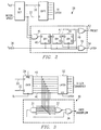
- Figure 1 is an electrical schematic diagram of a PLL circuit with non-linear gain according to a preferred embodiment of the invention for driving a motor connected to the PLL circuit.
- Figure 2 is an electrical schematic diagram of the edge detector circuit of Figure 1.
- Figure 3 is an electrical schematic diagram of the saturation detector of Figure 1.
- Figure 4 is an electrical schematic diagram of the lock detector of Figure 1.
- Figure 5 is a graph of the output voltage of the phase detector circuit as a function of the phase difference between the reference frequency and a motor speed signal, showing two gain operating ranges, according to the invention.
- FIG. 1 An electrical schematic block diagram of a digital AGC circuit 10 in which the apparatus and method according to the preferred embodiment of the invention may be incorporated is shown in Figure 1.
- the Figure 1 embodiment shows the subject matter of the invention and the associated processing and motor devices to provide a suitable context for the invention.
- the digital AGC circuit 10 provides different gains for use in a PLL circuit.
- the digital AGC circuit 10 can be constructed of discrete components, preferably it is integrated onto a single semiconductor chip adapted for connection into a PLL system. While PLL systems sometimes find particular application in motor driving circuits, it is to be appreciated that PLL circuits, and therefore the digital AGC circuit 10, may be employed in a variety of applications.
- the PLL circuit 10 embodiment shown in Figure 1 is used for driving a motor 12. Accordingly, standard motor driving circuitry is provided including a transconductance loop and other associated circuitry, denoted by the box 13 labeled "motor driver.” A signal is derived on a line 16 from the motor 12 and associated electronics that indicates the speed at which the motor 12 is rotating. The signal is referred to herein as the "motor speed signal.” The motor speed signal on the line 16 is connected to one input of a phase detector 18. A reference frequency signal is applied on a line 19 to another input of the phase detector 18 for comparison with the motor speed signal on the line 16. Thus, the frequency/phase detector 18, which may be, for example a commercially available phase detector, such as an MC4044 phase/frequency detector circuit, detects a phase difference between the two signals.
- the frequency/phase detector 18 which may be, for example a commercially available phase detector, such as an MC4044 phase/frequency detector circuit, detects a phase difference between the two signals.
- the frequency/phase detector 18 has two outputs, one on line 20 and the other on line 22.
- the output on the line 20 indicates that the reference frequency on line 19 leads the phase motor speed signal on line 16. This indicates that the motor speed is less than the desired speed, and needs to be increased.
- the output on the line 22 indicates that the phase motor speed signal on line 16 leads the reference frequency on line 19. This indicates that the motor speed exceeds the desired speed, and needs to be slowed.
- the frequency/phase detector 18 determines the time difference between the occurrence of the incoming pulse edges of the motor speed signal on line 16 and the reference frequency on line 19.
- the output on either line 20 or 22 from the frequency/phase detector 18 is a pulse of length equal or proportional to the time difference between the active edges of the pulses on lines 16 and 19.
- the pulses on lines 20 and 22 control the counter 24 to which they are respectively applied to count either up or down for that time. If the frequency/phase detector 18 detects the falling edge of a motor speed signal pulse on line 16 before it detects a falling edge of the reference frequency on line 19, it will emit a pulse on the "down" line 22 to control the counter 24 to count down.
- the frequency/phase detector 18 emits a pulse on the "up" line 20.
- the length of the frequency/phase detector 18 output pulse in any event is equal or proportional to the phase difference of the incoming signals.
- the counter 24 is connected to receive clock pulses on a line 25, the clock pulses being either at a system frequency, f SYS , or a divided system frequency, f SYS /N, as below described in greater detail.
- the counter 24 is connected to be preset to a predetermined mid-value count (for example, 10000000 in an 8-bit counter) by a preset signal on a line 53 from an edge detector circuit 28, also below described in greater detail.
- the outputs from the counter 24 on lines 40-40 are applied to a saturation detector 30.
- the saturation detector 30 produces an output signal on a line 33 for use in selecting the clock frequency applied to the counter 24, as below described.
- the function of the counter 24 can be performed by other types of counters. For instance, counters may be used that have a single input for counting either up or down depending on the sign of the pulse emitted from the phase detector 18. A qualifying gate pulse also may be provided to gate the clock in such embodiment.
- the clock signals applied to the counter 24 are received from a switch 35.
- the switch 35 has two positions. The first position connects the line 25 directly to the system frequency, f SYS , on input node 36. The other position connects the line 25 to a divided system frequency, f SYS /N, derived by a frequency divider 38.
- the clock signals provided by the switch 25 are determined by whether the counter is operating in a saturation condition, as determined by the saturation detector 30.
- the saturation detector 30 includes an AND gate 31 to the inputs of which each line 40-40 is connected. The output from the AND gate 31 is connected to one input of an OR gate 34. Additionally, a NOR gate 37 is provided to the inputs of which the lines 40-40 also are applied. The output from the NOR gate 37 is connected to another input of the OR gate 34.
- the output from the OR gate 34 represents the over/underflow, or saturation, signal that occurs when the counter 44 reaches a saturation state of either all ones or all zeros.
- the output from the saturation detector 30 is applied by an OR gate 42 to reset a "set-reset flip-flop 44."
- the Q output of the flip-flop 44 is connected to control the switch 35 to select either the system frequency, f SYS , directly from the node 36 or the divided system frequency, f SYS /N, from the frequency divider 38.
- the system frequency, f SYS or the divided system frequency, f SYS /N, clocks the counter 24.
- other reset conditions can be used to control the clocking frequency of the counter 24.
- a power on reset (POR) signal can be applied to the OR gate 42 also to serve to reset the flip-flop 44.
- the counter 24 When the counter 24 is reset, it is initialized to count up or down from an intermediate count value centered between its upper and lower saturation values. Thus, for example, if the counter 24 is an 8-bit counter, when it is reset, it may be initialized to the count 10000000, from which either an up or down count can be made. Additionally, the counter 24 is of the type that stops counting when an overflow or underflow condition occurs to hold at the over- or underflow count, instead of continuing to count, or wrapping around. For this purpose the clock signal 25 can be gated by the output of the saturation detector. The counter 24 is reset after the termination of the counting period generated by either signal on line 20 or line 22.
- the edge detector circuit 28 receives inputs from the up and down lines 20 and 22 at the inputs of a NAND gate 45.
- the output from the NAND gate 45 is connected to the D-input of a first D-type flip-flop 46.
- the Q output of the first D-type flip-flop 46 is connected to the D-input of a second D-type flip-flop 47, and to one input of a NOR gate 50.
- the output of the NOR gate 50 provides a "latch" signal on line 54 for use in the circuitry shown in Figure 1.
- the Q output of the second D-type flip-flop 47 is connected to the D-input of a third D-type flip-flop 48 and to one input of a NOR gate 49.
- the output of the NOR gate 49 on the line 53 is used to provide the "preset" signal to the circuitry shown in Figure 1.
- the Q(bar) output of the flip-flop 47 is connected to another input of the NOR gate 50.
- the Q(bar) output of the D-type flip-flop 48 is connected to another output of the NOR gate 49.
- the flip-flops 46, 47, and 48, as well as the NOR gates 49 and 50 are clocked by a system clock applied to the node 36.
- a data latch 52 receives on its inputs the data carried on lines 40-40 from the counter 24.
- the function of the latch 52 is enabled by a "latch" signal on the line 54 from the edge detector circuit 28, indicating completion of the phase difference measurement.
- the data output from the counter 24 is latched into the latch 52.
- the time in which the phase difference measurement is completed is, for example, when the falling edge of the last occurring pulse of the motor speed signal or the reference frequency occurs, as determined by the edge detector circuit 28.
- the output of the latch 52 developed upon lines 60-60 is applied to a digital-to-analog converter circuit 62.
- the current output from the digital-to-analog converter 62 is connected to the inverting input of an amplifier circuit 69.
- the amplifier circuit 69 includes an operational amplifier 68 having a resistor 76 connected to an analog ground 75 from its non-inverting input terminal, and a feedback resistor 72 connected between its output and the inverting input.
- the amplifier circuit 69 is biased by the resistor 76 so that the voltage applied to the inverting input by the digital to analog converter 62 is equal to the voltage on the analog ground 75 when the digital to analog converter 62 is driven by the "reset" value (for example, 10000000).
- the amplifier circuit 69 can be eliminated if the digital to analog converter 62 has a voltage output, by exchanging the lines 20 and 22 to the counter 24 to maintain the correct sign of the signal.
- the voltage output on the node 71 from the amplifier circuit 69 is applied to a filter circuit 80 and an integrator circuit 89 for application to the motor driver circuit 13.
- the integrator circuit 89 is of known construction, having an operational amplifier 86 and a resistor 94 connected between the non-inverting input terminal 92 and the analog ground 75.
- the output node 85 of the operational amplifier 86 is connected to the inverting input terminal by a capacitor 90 and resistor 88, connected in series.
- the output from the power driver circuit 13 is connected to the motor 12 to control its rotation.
- the set-reset flip-flop 44 is reset by the POR signal.
- the flip-flop 44 operates the switch 35 to select the divided system frequency, f SYS /N, produced at the output of the frequency divider 38.
- f SYS /N the divided system frequency
- a great difference will initially exist between the frequencies of the motor speed signal on the line 16 and the reference frequency on line 19.
- the counter 24 rapidly counts until it reaches saturation.
- the saturation detector circuit 30 continues a signal to the reset terminal of the flip-flop 44 to hold the flip-flop 44 in its reset state.
- the counter 24 counts the pulses until the end of the duration of the pulse on the line 20 or its own saturation. Then, the count of the counter 24 is latched into the latch 52. This binary number latched by the latch 52 is converted to an analog signal by the digital to analog converter 62 to produce an output voltage on the node 71.
- the gain at which the output voltage is produced on node 71 is relatively low, as shown by line 110 in Figure 5. Having a low gain during this time, or during a time in which lock may be lost for another reason, such as a temporary interruption or perturbation to the rotor of the motor 12, the low gain along line 110 assists in rapidly returning the circuit to a lock condition without significantly overshooting or over-correcting to achieve the lock condition (typically due to the saturation of the phase detector 18).
- the PLL circuit 10 when operated within the lock range (i.e., the reference frequency closely matches and tracks the frequency and phase of the motor frequency signal as determined by the lock detector circuit 61) the counter 24 no longer saturates between reset pulses from the edge detector 28.
- the determination that the circuit 10 is operating within a predetermined phase difference, herein the "lock range,” is determined by a lock detector circuit 61.
- the details of the lock detector circuit 61 are shown in Figure 4.
- the lock detector circuit 61 has two AND gates 63 and 64.
- the four most significant bits are compared with the fifth most significant bit to find whether the states on the 5 most significant bit lines within lines 60-60 are either "01111" or "10000,” to decide whether the count on lines 60-60 is within a predetermined range from the preset value (for example between 01111xxx and 10000xxx around the center count, 10000000).
- any desired lock range precision can be selected by the selection of the number of most significant bits compared by the AND gates 63 and 64.
- the outputs from the respective AND gates 63 and 64 are connected to the inputs of an OR gate 65, the output of which provides the "lock" signal on line 66.
- the detection of a lock condition by the detector 61 on line 66 is used to set the flip-flop 44.
- a series of D-type flip-flops 100, 103, . . . 104 may be provided, as shown.
- the output from the lock detector 61 is applied to the D-input of a first D-type flip-flop 101.
- the flip-flop 101 is clocked by the preset signal on line 53 developed by the edge detector circuit 28.
- the D-type flip-flop 101 is reset by the signal on the line 53 when the lock detector is producing no output. This condition is determined by AND gate 102.
- the number of similar flip-flops 103, . . . 104 determines the number of cycles in which lock is detected before the gain of the PLL is changed.
- the flip-flop 44 In the lock condition (or within the lock range as described above), as determined by the lock detector 61 and confirmed by passage through the series of D-type flip-flops 101, 103 . . . 104, the flip-flop 44 is set, thus commutating switch 35 to apply the system frequency, f SYS , from node 36 directly to clock the counter 24.
- the counter 24 produces a voltage on node 71 that follows the line 111 as shown in Figure 5. It can therefore be seen that in the lock range, the circuit 10 has a higher gain throughout the range of the counter 24, due to the difference in the clocking frequency.
- multiple break points can be provided, if desired, by using a counter (not shown) in place of the flip-flop 44 and multiple dividers (also not shown) in conjunction with divider 38, so that in each range, a "set” pulse moves into a higher frequency range, and a “reset” returns to the previous, lower frequency, range.
- the output range of the digital to analog converter 62 may also be changed by the Q output of the flip-flop 44, if appropriate for system stability.
Landscapes
- Control Of Electric Motors In General (AREA)
- Stabilization Of Oscillater, Synchronisation, Frequency Synthesizers (AREA)
- Feedback Control In General (AREA)
Claims (16)
- Circuit pour changer automatiquement le gain d'un PLL (10) pour piloter un moteur (12) du type comprenant un signal de vitesse de moteur (16) qui indique la vitesse de rotation du moteur, comprenant :un détecteur de phase (18) pour détecter la différence de phase entre le signal de vitesse de moteur (16) et une fréquence de référence (FREF) et pour produire un signal de sortie (20, 22) de durée proportionnelle à la différence de phase détectée ;un compteur (24) ;un circuit de commande de moteur (13, 89) pour commander le moteur (12) en réponse au comptage atteint par le compteur (24) par l'intermédiaire de la durée du signal de sortie du détecteur de phase (20, 22) ;une source d'impulsions d'horloge à une première fréquence (FSYS) et à une seconde fréquence, la seconde fréquence étant inférieure à la première fréquence (FSYS) ;un circuit de détection de plage de verrouillage (61) pour fournir un signal de sortie de détection (66) qui indique quand le PLL est à l'intérieur d'une plage de différence de phase prédéterminée ; etun circuit (35, 30, 33, 24, 44) agissant en réponse au signal de sortie de détection (66) pour appliquer sélectivement la première fréquence (FSYS) pour déclencher le compteur (24) quand le PLL est à l'intérieur de la plage de différence de phase prédéterminée, et pour appliquer sélectivement une seconde fréquence pour déclencher le compteur (24) quand le PLL fonctionne hors de la plage de différence de phase prédéterminée.
- Circuit selon la revendication 1, comprenant en outre un détecteur à saturation (30) pour produire un signal de saturation (33) quand le compteur (24) est en saturation, ledit circuit (35, 30, 33, 24, 44) agissant en réponse au signal de sortie de détection (66) pour appliquer sélectivement la seconde fréquence pour déclencher le compteur (24) en réponse au signal de saturation (33).
- Circuit selon la revendication 2, dans lequel le circuit agissant en réponse au signal de sortie de détection (66) pour appliquer sélectivement la première fréquence (FSYS) pour déclencher le compteur (24) et agissant en réponse au signal de saturation (33) pour appliquer la seconde fréquence pour déclencher le compteur (24) comprend une bascule (44) qui est mise à un par le signal de sortie de détection (66) et remise à zéro par le signal de saturation (33), une sortie de la bascule (44) étant connectée pour sélectionner la première (FSYS) ou la seconde fréquence en réponse au fait que la bascule (44) est mise à un ou remise à zéro.
- Circuit selon l'une quelconque des revendications 1 à 3, comprenant en outre une bascule (52) connectée pour recevoir le comptage atteint par le compteur (24) et un circuit (28) pour déterminer la durée du signal de sortie (20, 22) du détecteur de phase (18) et ayant une sortie connectée à la bascule (52) pour maintenir le comptage atteint par le compteur (24).
- Circuit selon la revendication 4, dans lequel le circuit de détection de plage de verrouillage (61) est connecté pour recevoir une sortie (60) de la bascule (52) pour produire un signal de sortie de détection (66) qui indique si le PLL est à l'intérieur de la plage de différence de phase prédéterminée.
- Circuit selon la revendication 5, dans lequel le circuit de détection de plage de verrouillage (61) est connecté pour détecter les états sur un nombre prédéterminé de lignes de sortie (60) en provenance de la bascule (52).
- Circuit selon la revendication 6, comprenant en outre un circuit de retard (101, 103, 104) auquel la sortie (66) du circuit de détection de plage de verrouillage (61) est appliquée, le circuit de retard (101, 103, 104) ayant une sortie connectée pour sélectionner la première séquence (FSYS) seulement après que le circuit de détection de plage de verrouillage (61) a détecté que le PLL est à l'intérieur de la plage de différence de phase prédéterminée sur un nombre prédéterminé de comparaisons entre le signal de vitesse de moteur (16) et la fréquence de référence (FREF).
- Circuit selon la revendication 7, dans lequel le circuit de retard (101, 103, 104) comprend plusieurs circuits de bascule (101, 103, 104).
- Circuit selon la revendication 8, dans lequel les divers circuits de bascule (101, 103, 104) comportent un premier circuit de bascule pour chaque nombre dudit nombre prédéterminé de comparaisons entre le signal de vitesse de moteur (16) et la fréquence de référence (FREF).
- Circuit selon l'une quelconque des revendications 1 à 9, dans lequel la source d'impulsions d'horloge comprend une source d'impulsions d'horloge à la première fréquence (FSYS) et un diviseur de fréquence (38) pour recevoir les impulsions d'horloge à la première fréquence (FSYS) et produire une sortie à une seconde fréquence divisée à partir de la première fréquence (FSYS).
- Circuit selon l'une quelconque des revendications 1 à 10, dans lequel le détecteur de phase (18) produit une impulsion en réponse à une comparaison entre le signal de vitesse de moteur (16) et la fréquence de référence (FREF) sur une première ligne (20) si le signal de vitesse de moteur (16) est en retard par rapport à la fréquence de référence (FREF) et sur une seconde ligne (22) si le signal de vitesse de moteur (16) est en avance sur la fréquence de référence (FREF).
- Circuit selon la revendication 11, dans lequel les première (20) et seconde (22) lignes du détecteur de phase (18) sont connectées pour provoquer des comptages vers le haut et vers le bas du compteur (24).
- Circuit selon l'une quelconque des revendications précédentes, comprenant en outre un circuit (28) pour préétablir le compteur (24) à une valeur de milieu de plage après la durée de chacun des signaux de sortie (20, 22) du détecteur de phase (18).
- Circuit selon l'une quelconque des revendications précédentes, dans lequel le circuit de commande de moteur (13, 89) comprend un filtre intégrateur (89) et une commande de moteur (13).
- Procédé pour changer automatiquement le gain d'un PLL (10) pour piloter un moteur (12) du type comprenant un signal de vitesse de moteur (16) qui indique la vitesse de rotation du moteur, comprenant les étapes suivantes :produire un signal de durée proportionnelle à la différence de phase entre le signal de vitesse de moteur (16) et une fréquence de référence (FREF) ;valider un compteur (24) pour compter des impulsions d'horloge (25) pendant la durée du signal (20, 22) de durée proportionnelle à la différence de phase ;piloter le moteur (12) pour fonctionner à une vitesse liée au comptage du compteur (24) ;détecter si le PLL (10) est à l'intérieur d'une plage de différence de phase prédéterminée ; etcommander la fréquence des impulsions d'horloge (25) vers le compteur (24) pour qu'elle soit à une première fréquence (FSYS) à l'intérieur d'une plage de différence de phase prédéterminée et à une seconde fréquence à l'extérieur de la plage de différence de phase prédéterminée.
- Procédé selon la revendication 15, dans lequel l'étape de commande de la fréquence des impulsions d'horloge (25) vers le compteur (24) pour être à une première fréquence (FSYS) à l'intérieur d'une plage de différence de phase prédéterminée et à une seconde fréquence à l'extérieur de la plage de différence de phase prédéterminée comprend l'étape consistant à fournir la première fréquence (FSYS) à une fréquence plus élevée que la seconde fréquence.
Applications Claiming Priority (2)
| Application Number | Priority Date | Filing Date | Title |
|---|---|---|---|
| US07/890,944 US5293445A (en) | 1992-05-29 | 1992-05-29 | AGC with non-linear gain for PLL circuits |
| US890944 | 1992-05-29 |
Publications (3)
| Publication Number | Publication Date |
|---|---|
| EP0572161A2 EP0572161A2 (fr) | 1993-12-01 |
| EP0572161A3 EP0572161A3 (fr) | 1994-04-06 |
| EP0572161B1 true EP0572161B1 (fr) | 1998-07-29 |
Family
ID=25397371
Family Applications (1)
| Application Number | Title | Priority Date | Filing Date |
|---|---|---|---|
| EP93303873A Expired - Lifetime EP0572161B1 (fr) | 1992-05-29 | 1993-05-19 | CÔntrole automatique et non-linéaire du gain pour circuits à boucle à verrouillage de phase |
Country Status (4)
| Country | Link |
|---|---|
| US (1) | US5293445A (fr) |
| EP (1) | EP0572161B1 (fr) |
| JP (1) | JP3317460B2 (fr) |
| DE (1) | DE69319966T2 (fr) |
Families Citing this family (9)
| Publication number | Priority date | Publication date | Assignee | Title |
|---|---|---|---|---|
| DE69332229T2 (de) * | 1993-12-08 | 2003-01-23 | Thomson Consumer Electronics | Digital analog wandlung zum steuern eines oszillators in einem phasenregelkreis |
| US5572099A (en) * | 1994-09-30 | 1996-11-05 | Sgs-Thomson Microelectronics, Inc. | Motor speed control with current limit |
| US5543697A (en) * | 1994-10-27 | 1996-08-06 | Sgs-Thomson Microelectronics, Inc. | Circuit and method for controlling the speed of a motor |
| US5689162A (en) * | 1995-06-07 | 1997-11-18 | Sgs-Thomson Microelectronics, Inc. | Apparatus and method for current sensing for motor driver in pwm mode |
| US5723963A (en) * | 1995-06-07 | 1998-03-03 | Sgs-Thomson Microelectronics, Inc. | Apparatus and method for controlling transition between PWM and linear operation of a motor |
| US5764095A (en) * | 1996-03-06 | 1998-06-09 | Sgs-Thomson Microelectronics, Inc. | Nonlinear integrator |
| US6084364A (en) * | 1996-12-19 | 2000-07-04 | Stmicroelectronics, Inc. | Using different frequency clocks to clock counters of a driver circuit at spin-up and at regulation |
| US5898287A (en) * | 1997-07-23 | 1999-04-27 | Technicore, Inc. | Slip controlled induction motor using variable frequency transducer and method for controlling slip |
| US6265902B1 (en) * | 1999-11-02 | 2001-07-24 | Ericsson Inc. | Slip-detecting phase detector and method for improving phase-lock loop lock time |
Citations (2)
| Publication number | Priority date | Publication date | Assignee | Title |
|---|---|---|---|---|
| US4564794A (en) * | 1985-05-23 | 1986-01-14 | International Business Machines Corporation | Phase locked loop and a motor control servo |
| EP0571148A1 (fr) * | 1992-05-19 | 1993-11-24 | STMicroelectronics, Inc. | Circuit de commande automatique de gain non-linéaire pour utilisation dans une boucle à verrouillage de phase |
Family Cites Families (12)
| Publication number | Priority date | Publication date | Assignee | Title |
|---|---|---|---|---|
| US4104570A (en) * | 1976-10-12 | 1978-08-01 | Reliance Electric Company | Digital control system for motors |
| JPS53125581A (en) * | 1977-04-11 | 1978-11-01 | Hitachi Ltd | Phase controller |
| ATE13375T1 (de) * | 1981-04-22 | 1985-06-15 | Contraves Ag | Schaltung zum erzeugen einer sinusfoermigen synchronisierspannung fuer die zuendung von thyristoren. |
| JPS6047515A (ja) * | 1983-08-26 | 1985-03-14 | Victor Co Of Japan Ltd | 同期引込判別回路 |
| JPS60134310A (ja) * | 1983-12-22 | 1985-07-17 | Hitachi Ltd | モータ制御装置 |
| JPS60241784A (ja) * | 1984-05-15 | 1985-11-30 | Sanyo Electric Co Ltd | 直流サ−ボモ−タの制御装置 |
| JPS6240075A (ja) * | 1985-08-13 | 1987-02-21 | Toshiba Corp | Pll及びそれを用いたモ−タコントロ−ラ |
| GB8522998D0 (en) * | 1985-09-18 | 1985-10-23 | Plessey Co Plc | Phase comparator lock detect circuit |
| US4816937A (en) * | 1985-10-17 | 1989-03-28 | Canon Kabushiki Kaisha | Recording and/or reproduction apparatus capable of retaining start up information |
| JP2724142B2 (ja) * | 1986-12-19 | 1998-03-09 | 株式会社リコー | 回転速度信号発生装置 |
| US4827225A (en) * | 1988-06-13 | 1989-05-02 | Unisys Corporation | Fast locking phase-locked loop utilizing frequency estimation |
| GB2239112B (en) * | 1989-11-13 | 1993-12-08 | Mitsubishi Electric Corp | Brushless motor and an axial flow fan with the brushless motor |
-
1992
- 1992-05-29 US US07/890,944 patent/US5293445A/en not_active Expired - Lifetime
-
1993
- 1993-05-19 DE DE69319966T patent/DE69319966T2/de not_active Expired - Fee Related
- 1993-05-19 EP EP93303873A patent/EP0572161B1/fr not_active Expired - Lifetime
- 1993-05-28 JP JP12680893A patent/JP3317460B2/ja not_active Expired - Fee Related
Patent Citations (2)
| Publication number | Priority date | Publication date | Assignee | Title |
|---|---|---|---|---|
| US4564794A (en) * | 1985-05-23 | 1986-01-14 | International Business Machines Corporation | Phase locked loop and a motor control servo |
| EP0571148A1 (fr) * | 1992-05-19 | 1993-11-24 | STMicroelectronics, Inc. | Circuit de commande automatique de gain non-linéaire pour utilisation dans une boucle à verrouillage de phase |
Also Published As
| Publication number | Publication date |
|---|---|
| DE69319966T2 (de) | 1998-12-10 |
| JPH06233575A (ja) | 1994-08-19 |
| DE69319966D1 (de) | 1998-09-03 |
| US5293445A (en) | 1994-03-08 |
| EP0572161A3 (fr) | 1994-04-06 |
| JP3317460B2 (ja) | 2002-08-26 |
| EP0572161A2 (fr) | 1993-12-01 |
Similar Documents
| Publication | Publication Date | Title |
|---|---|---|
| EP0085615B1 (fr) | Circuit pour boucle d'asservissement de phase | |
| US4587496A (en) | Fast acquisition phase-lock loop | |
| JP3299636B2 (ja) | ジッタが補償される低電力の位相ロック・ループとその方法 | |
| US7372339B2 (en) | Phase lock loop indicator | |
| US5668503A (en) | System and method for calibrating damping factor or analog PLL | |
| US20060009184A1 (en) | Hybrid control of phase locked loops | |
| JP2503009B2 (ja) | デ−タ検出エラ−率測定装置 | |
| EP0572161B1 (fr) | CÔntrole automatique et non-linéaire du gain pour circuits à boucle à verrouillage de phase | |
| JPS58210725A (ja) | 位相ロツク・ル−プ | |
| US5329560A (en) | AGC circuit with non-linear gain for use in PLL circuit | |
| US5500627A (en) | Precision duty cycle phase lock loop | |
| US4560950A (en) | Method and circuit for phase lock loop initialization | |
| JPS626431B2 (fr) | ||
| US5610541A (en) | Reset signal generation method and apparatus for use with a microcomputer | |
| US5793825A (en) | Method and apparatus for extending an operating frequency range of an instantaneous phase-frequency detector | |
| EP1538451B1 (fr) | Boucle à verrouillage de phase comprenant un détecteur de fréquence programmable | |
| JPH11178380A (ja) | モータ速度制御装置 | |
| JPH01157123A (ja) | 周波数ロックループの周波数検出器 | |
| US6593815B2 (en) | Full digital phase locked loop and circuitry for utilizing the same | |
| JPS6363135B2 (fr) | ||
| JPS6310668B2 (fr) | ||
| EP0164806A2 (fr) | Circuit PLL | |
| EP0190578B1 (fr) | Discriminateur de phase pour une horloge | |
| JPS648541B2 (fr) | ||
| JPH0241026A (ja) | Pll回路 |
Legal Events
| Date | Code | Title | Description |
|---|---|---|---|
| PUAI | Public reference made under article 153(3) epc to a published international application that has entered the european phase |
Free format text: ORIGINAL CODE: 0009012 |
|
| AK | Designated contracting states |
Kind code of ref document: A2 Designated state(s): DE FR GB IT |
|
| PUAL | Search report despatched |
Free format text: ORIGINAL CODE: 0009013 |
|
| AK | Designated contracting states |
Kind code of ref document: A3 Designated state(s): DE FR GB IT |
|
| 17P | Request for examination filed |
Effective date: 19941004 |
|
| 17Q | First examination report despatched |
Effective date: 19960809 |
|
| GRAG | Despatch of communication of intention to grant |
Free format text: ORIGINAL CODE: EPIDOS AGRA |
|
| GRAG | Despatch of communication of intention to grant |
Free format text: ORIGINAL CODE: EPIDOS AGRA |
|
| GRAH | Despatch of communication of intention to grant a patent |
Free format text: ORIGINAL CODE: EPIDOS IGRA |
|
| GRAH | Despatch of communication of intention to grant a patent |
Free format text: ORIGINAL CODE: EPIDOS IGRA |
|
| GRAA | (expected) grant |
Free format text: ORIGINAL CODE: 0009210 |
|
| AK | Designated contracting states |
Kind code of ref document: B1 Designated state(s): DE FR GB IT |
|
| REF | Corresponds to: |
Ref document number: 69319966 Country of ref document: DE Date of ref document: 19980903 |
|
| ET | Fr: translation filed | ||
| RAP4 | Party data changed (patent owner data changed or rights of a patent transferred) |
Owner name: STMICROELECTRONICS, INC. |
|
| PLBE | No opposition filed within time limit |
Free format text: ORIGINAL CODE: 0009261 |
|
| STAA | Information on the status of an ep patent application or granted ep patent |
Free format text: STATUS: NO OPPOSITION FILED WITHIN TIME LIMIT |
|
| 26N | No opposition filed | ||
| PGFP | Annual fee paid to national office [announced via postgrant information from national office to epo] |
Ref country code: DE Payment date: 20000515 Year of fee payment: 8 |
|
| REG | Reference to a national code |
Ref country code: GB Ref legal event code: IF02 |
|
| PG25 | Lapsed in a contracting state [announced via postgrant information from national office to epo] |
Ref country code: DE Free format text: LAPSE BECAUSE OF NON-PAYMENT OF DUE FEES Effective date: 20020301 |
|
| PGFP | Annual fee paid to national office [announced via postgrant information from national office to epo] |
Ref country code: FR Payment date: 20040510 Year of fee payment: 12 |
|
| PGFP | Annual fee paid to national office [announced via postgrant information from national office to epo] |
Ref country code: GB Payment date: 20040519 Year of fee payment: 12 |
|
| PG25 | Lapsed in a contracting state [announced via postgrant information from national office to epo] |
Ref country code: IT Free format text: LAPSE BECAUSE OF NON-PAYMENT OF DUE FEES;WARNING: LAPSES OF ITALIAN PATENTS WITH EFFECTIVE DATE BEFORE 2007 MAY HAVE OCCURRED AT ANY TIME BEFORE 2007. THE CORRECT EFFECTIVE DATE MAY BE DIFFERENT FROM THE ONE RECORDED. Effective date: 20050519 Ref country code: GB Free format text: LAPSE BECAUSE OF NON-PAYMENT OF DUE FEES Effective date: 20050519 |
|
| GBPC | Gb: european patent ceased through non-payment of renewal fee |
Effective date: 20050519 |
|
| PG25 | Lapsed in a contracting state [announced via postgrant information from national office to epo] |
Ref country code: FR Free format text: LAPSE BECAUSE OF NON-PAYMENT OF DUE FEES Effective date: 20060131 |
|
| REG | Reference to a national code |
Ref country code: FR Ref legal event code: ST Effective date: 20060131 |