EP0561461B1 - Halbleiterschalter mit Temperaturfühler - Google Patents
Halbleiterschalter mit Temperaturfühler Download PDFInfo
- Publication number
- EP0561461B1 EP0561461B1 EP93200729A EP93200729A EP0561461B1 EP 0561461 B1 EP0561461 B1 EP 0561461B1 EP 93200729 A EP93200729 A EP 93200729A EP 93200729 A EP93200729 A EP 93200729A EP 0561461 B1 EP0561461 B1 EP 0561461B1
- Authority
- EP
- European Patent Office
- Prior art keywords
- region
- semiconductor device
- power semiconductor
- thermally responsive
- temperature
- Prior art date
- Legal status (The legal status is an assumption and is not a legal conclusion. Google has not performed a legal analysis and makes no representation as to the accuracy of the status listed.)
- Expired - Lifetime
Links
- 239000004065 semiconductor Substances 0.000 title claims description 108
- 230000003071 parasitic effect Effects 0.000 claims description 19
- 230000005669 field effect Effects 0.000 claims description 7
- 238000004891 communication Methods 0.000 claims description 3
- 238000001465 metallisation Methods 0.000 description 16
- 238000012986 modification Methods 0.000 description 10
- 230000004048 modification Effects 0.000 description 10
- 239000012535 impurity Substances 0.000 description 6
- 210000000746 body region Anatomy 0.000 description 4
- 230000007850 degeneration Effects 0.000 description 3
- 238000001514 detection method Methods 0.000 description 3
- 238000004519 manufacturing process Methods 0.000 description 3
- 238000010348 incorporation Methods 0.000 description 2
- 238000000034 method Methods 0.000 description 2
- 229910021420 polycrystalline silicon Inorganic materials 0.000 description 2
- 239000000758 substrate Substances 0.000 description 2
- 238000012935 Averaging Methods 0.000 description 1
- XUIMIQQOPSSXEZ-UHFFFAOYSA-N Silicon Chemical compound [Si] XUIMIQQOPSSXEZ-UHFFFAOYSA-N 0.000 description 1
- 230000015572 biosynthetic process Effects 0.000 description 1
- 230000000903 blocking effect Effects 0.000 description 1
- 229910052796 boron Inorganic materials 0.000 description 1
- -1 boron ions Chemical class 0.000 description 1
- 238000013461 design Methods 0.000 description 1
- 238000010586 diagram Methods 0.000 description 1
- 239000002019 doping agent Substances 0.000 description 1
- 238000002513 implantation Methods 0.000 description 1
- 238000002955 isolation Methods 0.000 description 1
- 239000000463 material Substances 0.000 description 1
- 229910021421 monocrystalline silicon Inorganic materials 0.000 description 1
- 230000035945 sensitivity Effects 0.000 description 1
- 238000000926 separation method Methods 0.000 description 1
- 229910052710 silicon Inorganic materials 0.000 description 1
- 239000010703 silicon Substances 0.000 description 1
Images

Classifications
-
- H—ELECTRICITY
- H01—ELECTRIC ELEMENTS
- H01L—SEMICONDUCTOR DEVICES NOT COVERED BY CLASS H10
- H01L29/00—Semiconductor devices adapted for rectifying, amplifying, oscillating or switching, or capacitors or resistors with at least one potential-jump barrier or surface barrier, e.g. PN junction depletion layer or carrier concentration layer; Details of semiconductor bodies or of electrodes thereof ; Multistep manufacturing processes therefor
- H01L29/66—Types of semiconductor device ; Multistep manufacturing processes therefor
- H01L29/68—Types of semiconductor device ; Multistep manufacturing processes therefor controllable by only the electric current supplied, or only the electric potential applied, to an electrode which does not carry the current to be rectified, amplified or switched
- H01L29/76—Unipolar devices, e.g. field effect transistors
- H01L29/772—Field effect transistors
- H01L29/78—Field effect transistors with field effect produced by an insulated gate
- H01L29/7801—DMOS transistors, i.e. MISFETs with a channel accommodating body or base region adjoining a drain drift region
- H01L29/7802—Vertical DMOS transistors, i.e. VDMOS transistors
- H01L29/7803—Vertical DMOS transistors, i.e. VDMOS transistors structurally associated with at least one other device
-
- G—PHYSICS
- G01—MEASURING; TESTING
- G01K—MEASURING TEMPERATURE; MEASURING QUANTITY OF HEAT; THERMALLY-SENSITIVE ELEMENTS NOT OTHERWISE PROVIDED FOR
- G01K7/00—Measuring temperature based on the use of electric or magnetic elements directly sensitive to heat ; Power supply therefor, e.g. using thermoelectric elements
- G01K7/16—Measuring temperature based on the use of electric or magnetic elements directly sensitive to heat ; Power supply therefor, e.g. using thermoelectric elements using resistive elements
- G01K7/18—Measuring temperature based on the use of electric or magnetic elements directly sensitive to heat ; Power supply therefor, e.g. using thermoelectric elements using resistive elements the element being a linear resistance, e.g. platinum resistance thermometer
- G01K7/20—Measuring temperature based on the use of electric or magnetic elements directly sensitive to heat ; Power supply therefor, e.g. using thermoelectric elements using resistive elements the element being a linear resistance, e.g. platinum resistance thermometer in a specially-adapted circuit, e.g. bridge circuit
-
- G—PHYSICS
- G01—MEASURING; TESTING
- G01K—MEASURING TEMPERATURE; MEASURING QUANTITY OF HEAT; THERMALLY-SENSITIVE ELEMENTS NOT OTHERWISE PROVIDED FOR
- G01K7/00—Measuring temperature based on the use of electric or magnetic elements directly sensitive to heat ; Power supply therefor, e.g. using thermoelectric elements
- G01K7/01—Measuring temperature based on the use of electric or magnetic elements directly sensitive to heat ; Power supply therefor, e.g. using thermoelectric elements using semiconducting elements having PN junctions
-
- H—ELECTRICITY
- H01—ELECTRIC ELEMENTS
- H01L—SEMICONDUCTOR DEVICES NOT COVERED BY CLASS H10
- H01L27/00—Devices consisting of a plurality of semiconductor or other solid-state components formed in or on a common substrate
- H01L27/02—Devices consisting of a plurality of semiconductor or other solid-state components formed in or on a common substrate including semiconductor components specially adapted for rectifying, oscillating, amplifying or switching and having at least one potential-jump barrier or surface barrier; including integrated passive circuit elements with at least one potential-jump barrier or surface barrier
- H01L27/0203—Particular design considerations for integrated circuits
- H01L27/0248—Particular design considerations for integrated circuits for electrical or thermal protection, e.g. electrostatic discharge [ESD] protection
-
- H—ELECTRICITY
- H01—ELECTRIC ELEMENTS
- H01L—SEMICONDUCTOR DEVICES NOT COVERED BY CLASS H10
- H01L27/00—Devices consisting of a plurality of semiconductor or other solid-state components formed in or on a common substrate
- H01L27/02—Devices consisting of a plurality of semiconductor or other solid-state components formed in or on a common substrate including semiconductor components specially adapted for rectifying, oscillating, amplifying or switching and having at least one potential-jump barrier or surface barrier; including integrated passive circuit elements with at least one potential-jump barrier or surface barrier
- H01L27/04—Devices consisting of a plurality of semiconductor or other solid-state components formed in or on a common substrate including semiconductor components specially adapted for rectifying, oscillating, amplifying or switching and having at least one potential-jump barrier or surface barrier; including integrated passive circuit elements with at least one potential-jump barrier or surface barrier the substrate being a semiconductor body
- H01L27/08—Devices consisting of a plurality of semiconductor or other solid-state components formed in or on a common substrate including semiconductor components specially adapted for rectifying, oscillating, amplifying or switching and having at least one potential-jump barrier or surface barrier; including integrated passive circuit elements with at least one potential-jump barrier or surface barrier the substrate being a semiconductor body including only semiconductor components of a single kind
- H01L27/085—Devices consisting of a plurality of semiconductor or other solid-state components formed in or on a common substrate including semiconductor components specially adapted for rectifying, oscillating, amplifying or switching and having at least one potential-jump barrier or surface barrier; including integrated passive circuit elements with at least one potential-jump barrier or surface barrier the substrate being a semiconductor body including only semiconductor components of a single kind including field-effect components only
- H01L27/088—Devices consisting of a plurality of semiconductor or other solid-state components formed in or on a common substrate including semiconductor components specially adapted for rectifying, oscillating, amplifying or switching and having at least one potential-jump barrier or surface barrier; including integrated passive circuit elements with at least one potential-jump barrier or surface barrier the substrate being a semiconductor body including only semiconductor components of a single kind including field-effect components only the components being field-effect transistors with insulated gate
-
- H—ELECTRICITY
- H01—ELECTRIC ELEMENTS
- H01L—SEMICONDUCTOR DEVICES NOT COVERED BY CLASS H10
- H01L29/00—Semiconductor devices adapted for rectifying, amplifying, oscillating or switching, or capacitors or resistors with at least one potential-jump barrier or surface barrier, e.g. PN junction depletion layer or carrier concentration layer; Details of semiconductor bodies or of electrodes thereof ; Multistep manufacturing processes therefor
- H01L29/02—Semiconductor bodies ; Multistep manufacturing processes therefor
- H01L29/06—Semiconductor bodies ; Multistep manufacturing processes therefor characterised by their shape; characterised by the shapes, relative sizes, or dispositions of the semiconductor regions ; characterised by the concentration or distribution of impurities within semiconductor regions
- H01L29/0684—Semiconductor bodies ; Multistep manufacturing processes therefor characterised by their shape; characterised by the shapes, relative sizes, or dispositions of the semiconductor regions ; characterised by the concentration or distribution of impurities within semiconductor regions characterised by the shape, relative sizes or dispositions of the semiconductor regions or junctions between the regions
- H01L29/0692—Surface layout
- H01L29/0696—Surface layout of cellular field-effect devices, e.g. multicellular DMOS transistors or IGBTs
-
- H—ELECTRICITY
- H01—ELECTRIC ELEMENTS
- H01L—SEMICONDUCTOR DEVICES NOT COVERED BY CLASS H10
- H01L29/00—Semiconductor devices adapted for rectifying, amplifying, oscillating or switching, or capacitors or resistors with at least one potential-jump barrier or surface barrier, e.g. PN junction depletion layer or carrier concentration layer; Details of semiconductor bodies or of electrodes thereof ; Multistep manufacturing processes therefor
- H01L29/40—Electrodes ; Multistep manufacturing processes therefor
- H01L29/41—Electrodes ; Multistep manufacturing processes therefor characterised by their shape, relative sizes or dispositions
- H01L29/417—Electrodes ; Multistep manufacturing processes therefor characterised by their shape, relative sizes or dispositions carrying the current to be rectified, amplified or switched
- H01L29/41725—Source or drain electrodes for field effect devices
- H01L29/41766—Source or drain electrodes for field effect devices with at least part of the source or drain electrode having contact below the semiconductor surface, e.g. the source or drain electrode formed at least partially in a groove or with inclusions of conductor inside the semiconductor
Definitions
- This invention relates to a semiconductor switch comprising a power semiconductor device and a temperature sensor.
- US-A-4730228 describes a temperature sensing circuit in which the temperature of a power semiconductor device is sensed by a bipolar transistor.
- the bipolar transistor is arranged in series with the main conductive path of a depletion mode (normally off) insulated gate field effect transistor (IGFET or MOSFET).
- the bipolar transistor has an open base connection and is in thermal contact with the power semiconductor device.
- the bipolar transistor may be provided in the same semiconductor body as the power semiconductor device within a recess in the power semiconductor device.
- the depletion mode IGFET may also be integrated in the same semiconductor body but at a location remote from the power semiconductor device.
- the thermally responsive semiconductor device is provided by a number of device cells similar, generally identical, to the device cells forming the power semiconductor device so that very little modification of the mask set used to produce the power semiconductor device is required to allow incorporation of the thermally responsive device.
- each further device cell is connected to its third region or to a third region of the power semiconductor device.
- the insulated gate of each further device cell may be electrically shorted to the third region by a simple modification of the mask used to define the metallisation level.
- the second and third regions of the further device cells may be electrically shorted so as to provide a base-emitter shorted parasitic bipolar transistor. This should provide an improved output and higher signal. This can be achieved very simply as it is conventional in the manufacture of a power insulated gate field effect such as a power MOSFET or IGBT (Insulated Gate Bipolar Transistor) for the source (third) region to be shorted to the body (the channel-defining second region) and accordingly no mask modification is necessary to achieve the emitter-base short. Alternatively by modification of the appropriate masks, the second regions of the further device cells may be left floating so as to define an open base parasitic bipolar transistor.
- a power insulated gate field effect such as a power MOSFET or IGBT (Insulated Gate Bipolar Transistor)
- IGBT Insulated Gate Bipolar Transistor
- At least the power semiconductor device second regions may each have a more highly doped central area. In the case of the power insulated gate field effect device this serves to facilitate good contact by the metallisation and to improve ruggedness.
- the further device cells may be provided adjacent the periphery of the power semiconductor device which should simplify the affect of any metallisation modifications.
- the further device cells may be provided amongst the device cells forming the power semiconductor device so enabling a more accurate detection of the temperature of the power semiconductor device. This can be achieved relatively simply in the present case without detrimentally affecting device yield because the thermally responsive device is made up of device cells similar, generally identical, to those of the power semiconductor device. It may even be possible for the further device cells forming the thermally responsive device to be distributed throughout the power semiconductor device (e.g. with a number of further cells at two or more different locations) although the current sharing of the power semiconductor device will normally be so good that this would not significantly increase the accuracy of detection of the thermal condition of the power semiconductor device.
- the further device cells may be provided in a linear or any similar arrangement which maximises the ratio between the periphery of and the area occupied by the thermally responsive semiconductor device so as to increase its sensitivity to temperature changes.
- the temperature sensor will be arranged to detect when the temperature of the power semiconductor device reaches a predetermined value.
- the temperature sensor may be used, provided the rate of charge of voltage across the semiconductor body is small, to detect the temperature difference between centre cells and edge cells of the power device.
- the temperature sensor may comprise a further thermally responsive device similar to the thermally responsive semiconductor device, one of the thermally responsive semiconductor devices being provided adjacent and the other remote from the power semiconductor device and the temperature sensor may comprise means responsive to the two thermally responsive devices for providing a control signal to switch off the power semiconductor device when the difference in the temperatures sensed by the two thermally responsive semiconductor devices exceeds a predetermined value.
- One thermally responsive device may be provided adjacent the periphery of or actually within the power semiconductor device and the other thermally responsive device may be further from the periphery so enabling the temperature difference between the two thermally responsive devices to be determined.
- the temperature at the centre of the power semiconductor device rises much more quickly than that of the surrounding semiconductor body so that a steep temperature gradient occurs at the periphery of the active semiconductor device.
- the use of two spaced thermally responsive devices allows this steep temperature gradient to be detected and to be used to provide a signal to switch off the active semiconductor device before it overheats significantly. Accordingly, excessive temperatures can be detected quickly and the circuit can be particularly sensitive to temperature changes.
- the switch of the present invention also may be integrated with a temperature sensing circuit comprising first and second transistors connected in a current mirror arrangement, a current source connected in series with the first and second transistors and the thermally responsive device in thermal communication with the power semiconductor device, the thermally responsive device passing a current which increases with temperature and being connected to an auxiliary current source for the second transistor for causing the second transistor to become increasingly switched off as the temperature sensed, and thus the current passed, by the thermally responsive device increases until the temperature sensor provides a control signal for switching off the power semiconductor device when the predetermined thermal condition exists.
- Figures 2 and 3 are merely schematic and are not drawn to scale. In particular certain dimensions such as the thickness of layers or regions may have been exaggerated whilst other dimensions may have been reduced. It should also be understood that the same reference numerals are used throughout the Figures to indicate the same or similar parts.
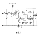
- a semiconductor switch comprising a power semiconductor device 1 and a temperature sensor 2 for providing a control signal to switch off the power semiconductor device 1 when the power semiconductor device 1 has a predetermined thermal condition, for example when the temperature sensor 2 senses that the power semiconductor device 1 has reached a predetermined temperature.
- the power semiconductor device 1 comprises a semiconductor body 10 having a first region 13 of one conductivity type adjacent one major surface 10a and a plurality of device cells 11 forming an insulated gate field effect device each cell 11 comprising a second region 32 of the opposite conductivity type provided within the first region 13, a third region 33 of the one conductivity type provided within the second region 32 and an insulated gate 34 overlying a conduction channel region 35 of the second region 32 for providing a gateable conductive path between the third and first regions 33 and 13.
- the temperature sensor 2 comprises a thermally responsive semiconductor device 100 formed within the semiconductor body 10 and comprising a number of further device cells 11' with each further device cell comprising a second region 32 provided within the first region 13, a third region 33 provided within the second region and an insulated gate 34 overlying a conduction channel region 35 of the second region of the further device cell 11'.
- the insulated gate 34 of each further device cell 11' is electrically connected to a third region, either the third region 33 of the further device cell 11' or a third region of the power semiconductor device 1, so that the further device cells 11' provide a parasitic bipolar P transistor having a leakage current which varies with temperature for enabling the temperature sensor 2 to provide the control signal to switch off the power semiconductor device 1 when the predetermined thermal condition exists.
- the thermally responsive semiconductor device 100 is provided by a number of device cells 11' similar, generally identical, to the device cells 11 forming the power semiconductor device 1 so that very little modification of the mask set used to produce the power semiconductor device 1 is required to allow incorporation of the thermally responsive device 100.
- Figure 1 illustrates one example of a temperature sensing circuit 2 which incorporates the thermally responsive device 100 mentioned above and which is used to provide a control signal to switch off the power semiconductor device 1 shown in Figure 2 when the temperature sensed by the thermally responsive device 100 reaches the predetermined temperature.
- the circuit 2 comprises first and second transistors Q1 and Q2 connected in a current mirror arrangement and a current source R2,R4 connected in series with the first and second transistors Q1 and Q2.
- the thermally responsive device 100 in thermal communication with the power semiconductor device 1 passes a current which increases with temperature and is connected to an auxiliary current source R5 for the second transistor Q2 for causing the second transistor Q2 to become increasingly switched off as the temperature sensed, and thus the current passed, by the thermally responsive device 100 increases until, at the predetermined temperature, the temperature sensor provides a control signal for switching off the power semiconductor device 1.
- a respective current source R2,R4 is connected in series with each of the first and second transistors Q1 and Q2, and the thermally responsive device 100 is connected in series with a resistor R5 connected in parallel with the current source R4 of the second transistor Q2.
- the current passed by the thermally responsive device 100 is used to offset the current in the source degeneration resistor R5 connected to the current mirror arrangement R2,R4.
- the temperature sensing circuit 2 has first and second power supply lines 3 and 4.
- the first and second transistors Q1 and Q2 are both n-channel enhancement mode (normally off) IGFETs (insulated gate field effect transistors) having their first (drain) main electrodes connected via respective resistors R1 and R2 to the first power supply line 3 and their second (source) main electrodes connected to the second power supply line 4, which is in this example earth.
- the control or gate electrodes of the first and second transistors Q1 and Q2 are connected together and the control electrode of the first transistor Q1 is connected to its drain electrode to form a current mirror arrangement.
- the back gates of the first and second transistors Q1 and Q2 are not connected to their respective sources in the normal manner but are connected to earth (ground), that is to the second power supply line 4.
- this connection is shown merely by an earth symbol on the back gates and not by an actual connection line to the second power supply line 4.
- the back gates of transistors Q1 and Q2 could be connected to their respective sources in normal manner although this might require some adjustment of the circuit parameters.
- a respective current source connects the source electrode of each of the transistors Q1 and Q1 to the second power supply line 4.
- the current sources could be of any suitable form but in this example are provided as resistors R2 and R4 which may be of the type to be described below with reference to Figure 3.
- resistors R2 and R4 which may be of the type to be described below with reference to Figure 3.
- diode-connected depletion mode IGFETs could be used.
- a further resistor R5 is connected in parallel with the resistor R4 and acts as a current source degeneration resistor for the transistor Q2 so that, as will be explained below, at normal temperatures of the power semiconductor device 1 the current drawn by transistor Q2 is not equal to that drawn by transistor Q1.
- any suitable form of current source may be used in place of the resistor R5.
- the thermally responsive device 100 comprises, as will be explained in greater detail below with reference to Figures 2 and 3, a small power MOSFET formed by a number of device cells 11' formed in the same semiconductor body 10 as the power MOSFET 1 whose temperature is to be detected.
- the power MOSFET 1 is an n-channel enhancement mode MOSFET and the thermally responsive device 100 is therefore also an n-channel enhancement mode MOSFET.
- the gate electrode of the thermally responsive device 100 is connected to its source electrode as shown in Figure 1 so that the thermally responsive device 100 is provided by a parasitic bipolar transistor P within the small power MOSFET.
- the parasitic bipolar transistor P has, in this case, its base and emitter regions shorted by virtue of the fact that the source metallisation of the power MOSFET 1 shorts its third or source regions 33 to the channel-defining second or body regions 32. This should enable a higher gain and thus higher output than could be achieved with an open (or floating) base arrangement. However by appropriate modification of the metallisation mask, the parasitic bipolar transistor P may have a floating base.
- the power MOSFET 1 itself forms a low-side switch having its drain electrode connected via a load L, for example a light bulb, to a positive power supply line 5.
- the gate electrode of the power MOSFET 1 is connected to an input control line 7 which receives, via an appropriate input circuit, signals for controlling switching on and off of the power MOSFET 1.
- the input circuit comprises series-connected resistors R9 and R10 and a zener diode D1 connected between the node between the two resistors R9 and R10 and the power supply line 4.
- the zener diode D1 serves to protect the insulated gate 34 of the power semiconductor device 1.
- the source electrode of the thermally responsive device 100 is connected in series with the source degeneration resistor R5 so that, as will be described below, the thermally responsive device 100 provides an additional current source for the transistor Q2.
- the drain electrode of the second transistor Q2 is connected at junction W to the gate electrode of an n-channel enhancement mode third IGFET Q3 having its drain electrode connected via a fourth resistor R6 to the first power supply line 3 and its source electrode connected via a fifth resistor R8 to the second power supply line 4.
- the drain electrode of the third IGFET Q3 is connected to the gate electrode of a fourth n channel enhancement mode IGFET Q4 having its drain electrode connected via a resistor R7 to the first power supply line 3 and having its source electrode connected to the second power supply line 4.
- the two transistors Q3 and Q4 form an inverting output stage as will be discussed below.
- the drain electrode of IGFET Q4 is connected to a further n-channel enhancement mode IGFET Q5 which has its source electrode connected to the second power supply line 4.
- the IGFET Q5 forms an output transistor and its drain electrode is connected via an output line 6 and the resistor R10 to the insulated gate 34 of the power semiconductor device 1.
- Figure 2 illustrates a top plan view of part of the semiconductor body 10 within which the power MOSFET 1 and the thermally responsive device or auxiliary MOSFET 100 are formed while Figure 3 illustrates a cross-sectional view through part of the semiconductor body 10.
- the power MOSFET 1 comprises a plurality of device or source cells 11 each of which comprises a second or body region 32, a third or source region 33 within the second region 32 so that the second and third regions 32 and 33 define therebetween a conduction channel region 35 (see Figure 3) over which the insulated gate 34 extends between each third region 33 and the first region 13 which forms at least part of a common drain region.
- Each second region 32 has a relatively deep relatively highly doped central region 32a which extends up to the surface 10a within the associated source region 33 to enable the source region 33 to be shorted to the second region 32 in normal manner to enable good contact by the source metallisation and to improve the ruggedness of the device.
- the power MOSFET 1 may consist of many hundreds of thousands of source cells 11.
- the periphery 34a of the insulated gate 34 may extend up onto field oxide 15 surrounding the edge of the power MOSFET 1 in conventional manner and, although not shown, conventional edge termination such as Kao's rings and/or field plates may be provided at the periphery of the power MOSFET 1.
- the thermally responsive device 100 effectively comprises a much smaller version of the power MOSFET 1.
- the thermally responsive device comprises 49 source cells 11' each formed by a second region 32 containing a third region 33 and defining with the third or source region 33 a conduction channel 35 (see Figure 3) over which the insulated gate 34 extends between each third region 33 and the first region 13 which forms at least part of a common drain region of the auxiliary MOSFET.
- a central region 32a of each second region 32 extends to the surface 10a within each source cell 11'.
- the number of source cells 11' forming the thermally responsive device 100 will of course depend on the desired characteristics and could be more or less than shown.
- the insulated gate of the thermally responsive device 100 is connected directly to its source electrode. This can be achieved simply by modifying the metallisation mask in the area of the thermally responsive device 100 so that there is no separation of the source and gate metallisation of the thermally responsive device.
- the auxiliary MOSFET 100 thus provides a parasitic bipolar transistor P in which the source and body regions 33 and 32 provide the emitter and base regions and the common first region 13 provides the collector region of the bipolar transistor P.
- the parasitic bipolar P has its base shorted to its emitter.
- Figure 3 illustrates, by way of a cross-section through the semiconductor body 10, typical structures for the source cells 11 and 11' of the MOSFETs 1 and 100.
- Figure 3 shows typical structures for the resistors R1 to R8 and the n-channel IGFETs Q1 to Q5. It will be appreciated that only one resistor R1 and one IGFET Q1 are shown in Figure 3 because the structures of the resistors R1 to R8 and all the IGFETs Q may be similar.
- the structures of the source cells 11 and 11' of the power MOSFET 1 and the thermally responsive device 100 are also similar the cross-section of only one source cell 11,11' is shown.
- the semiconductor body 10 comprises a relatively high doped n conductivity type monocrystalline silicon substrate 10b onto which is provided a relatively lowly doped n conductivity type epitaxial layer which forms the first region 13.
- the relatively highly doped substrate 10b provides a drain contact region which makes ohmic contact to metallisation 17 on the other major surface 10c of the semiconductor body 10.
- the metallisation 31 forms at least part of the connected drain electrodes of the power MOSFET 1 and the thermally responsive device 100.
- the resistors R1 to R8 may have any suitable form and could be, for example, simple diffused resistors or doped polycrystalline silicon resistors.
- the resistors R1 to R8 are formed in the first region 13 of the semiconductor body 10 by a region 20 of the opposite conductivity type formed within the first region 13 and a further region 21 of the one conductivity type formed within the second region 20, first and second electrodes 22 and 23 being spaced apart on the third region 21 so that a resistive path is provided by the third region 21 between the first and second electrodes 22 and 23.
- a reference electrode 24 is provided for connecting the region 20 to a reference potential, the second power supply line 4 in this example.
- the region 20 is formed as a planar region by introducing, using an appropriate mask, p conductivity type impurities, generally boron ions with a dose (which determines the surface concentrations) in the region 10 x 10 12 to 13 x 10 12 atoms cm -2 , while the region 21 is formed as a planar region within the region 20 by introducing impurities using an appropriate mask with a dose in the region of 2 x 10 12 to 3 x 10 12 atoms cm -2 .
- the impurity concentrations within the regions 20 and 21 are such that the temperature coefficients of resistance of the diffused resistor formed by the third region 21 and the junction field effect transistor like structure formed by the regions 20 and 21 counteract to provide the resistor with a temperature coefficient of resistance ⁇ which increases with absolute temperature such that the relative temperature coefficient of resistance referred to the sensed temperature is substantially constant.
- the n-channel enhancement transistors Q1 to Q5 may have any suitable form.
- each transistor Q1 to Q5 is a lateral IGFET and may have the structure shown in Figure 3 where the n-channel IGFET Q1 (for example) is formed in a relatively lowly doped p conductivity type isolation well having a surface dopant concentration of the order of 2-3 x 10 12 atoms cm -2 which is connected to the second supply line 4 (generally earth) via an electrode.
- the lateral IGFETs Q1 to Q5 may be formed in the same region 20 as the resistors R1 to R8 so that the electrode 24 provides the back gate connection to the second supply line 4.
- the source and drain regions 40 and 41 of the IGFETs Q1 to Q5 may be formed with the source regions 33.
- the insulated gates 34 of the MOSFETs 1 and 100 and the insulated gates 42 of the IGFETs Q1 to Q5 are first defined after definition of any field oxide 15 and formation of the region 20.
- the insulated gates will comprise a thermal gate oxide layer followed by a doped polycrystalline silicon layer. Impurities for forming the relatively deep relatively highly doped central regions 32a may then be introduced (with the areas of the IGFETs Q1 to Q5 and resistors covered) with the mask used to define the insulated gates still in place. This mask will overhang the insulated gates so that the central regions 24a will be spaced from the insulated gates.
- the insulated gates 34 form at least part of the mask for forming the regions 32 and 33 so that these regions 32 and 33 are autoaligned to the insulated gates 34.
- each source region 33 may be masked during the implantation process or may be subsequently etched away as shown in Figure 3 to allow the source metallisation 36 to contact the central regions 32a. As indicated above, if it is desired for the base of the parasitic bipolar transistor P to be floating rather than shorted to the emitter the central area of the source regions 33 of the auxiliary MOSFET 100 will not be so masked or etched.
- An insulating layer 37 is then provided and contact holes opened to enable metallisation to be deposited and defined to provide the source electrodes 36 and gate electrodes (not shown) of the MOSFETs 1, the shorted source-gate metallisation of the auxiliary MOSFET 100, the electrodes 22 to 24 of the resistors R1 to R8 and the source, gate and drain electrodes of the IGFETs Q1 to Q5 plus appropriate interconnections in accordance with the circuit shown in Figure 1.
- the metallisation 17 is also provided on the other major surface 10c to form the drain electrodes of the MOSFETs 1, 100.
- the thermally responsive device 100 comprises a base-emitter shorted parasitic bipolar transistor P provided by a few device cells 11' of the power MOSFET 1.
- the cells 11' forming the transistor P are at the edge of the power MOSFET 1 to facilitate contact but they could be at the centre of the power MOSFET 1, so as to enable a faster and more accurate detection of the maximum temperature within the power MOSFET 1.
- the transistor P could be formed by a group of cells 11' remote from the power MOSFET 1 but formed at the same time.
- the parasitic bipolar transistor P senses or experiences the temperature of the power MOSFET 1 and the current through the base-emitter shorted bipolar transistor increases with the temperature of the power MOSFET 1. Typically, the current supplied by the parasitic bipolar transistor P will effectively double for each ten degree Celsius increase in temperature.
- the parasitic bipolar P supplies current for the source-degeneration resistor R5 which allows the voltage at junction X in Figure 1 to increase as the temperature sensed (and thus the current supplied) by the parasitic bipolar transistor P increases until the voltage at junction X equals the voltage at point Y so that the drain currents of the current-mirror connected transistors Q1 and Q2 are equal.
- the IGFET Q2 will become increasingly turned off and the voltage at junction W will rise to turn on IGFET Q3 and thus switch off IGFET Q4 so that the gate voltage of the IGFET Q5 rises causing the IGFET Q5 to turn on (or conduct) so as to pull the gate voltage of the power MOSFET 1 down towards the voltage of the second power supply line 4 and thus switch off the power MOSFET 1 once a predetermined temperature is exceeded.
- the actual predetermined temperature at which the circuit 2 provides an output signal to switch off the power MOSFET 1 will of course depend upon the particular nature of the various circuit components but may be, typically, a temperature in the range of from 180°C to 190°C (degrees Celsius).
- the parasitic npn bipolar transistor P has a high voltage blocking capability, and this method for detecting the leakage current enhances the useful lower working range of the sensor.
- the parasitic bipolar transistor P may be used in temperature sensing circuits other than that described with reference to Figure 1, for example in circuits similar to that described in US-A-4730228 or in EP-A-360333 (PHB33491). Furthermore, two or more such parasitic bipolar transistors P may be provided in the same semiconductor body as a power MOSFET to for example provide a more accurate assessment of temperature by measuring and averaging the temperatures at different locations or to provide a differential temperature sensing circuit. For example parasitic bipolar transistors P may be used to form the temperature sensing devices of differential temperature sensing circuit such as those described in EP-A-479362.
- the conductivity types, and where appropriate the polarities, given above could be reversed.
- the power semiconductor device 1 and thermally responsive device 100 could be lateral rather than vertical devices.
- semiconductor materials other than or in addition to silicon may be possible to use.
Claims (8)
- Halbleiterschalter, welcher eine Leistungshalbleiteranordnung (1) und einen Temperaturfühler (2) aufweist, um ein Steuersignal zum Abschalten der Leistungshalbleiteranordnung vorzusehen, sobald sich die Leistungshalbleiteranordnung in einem zuvor festgelegten, thermischen Zustand befindet, wobei die Leistungshalbleiteranordnung einen Halbleiterkörper (10) mit einer ersten Zone (13) eines ersten Leitfähigkeitstyps in Angrenzung an eine Hauptoberfläche (10a) sowie mehrere Bauelementzellen (11) aufweist, welche eine Feldeffektanordnung mit isoliertem Gate bilden, wobei jede Zelle eine, in der ersten Zone vorgesehene, zweite Zone (32) des entgegengesetzten Leitfähigkeitstyps, eine, in der zweiten Zone vorgesehene, dritte Zone (33) des ersten Leitfähigkeitstyps sowie ein, über einer Leitungskanalzone (35) der zweiten Zone liegendes, isoliertes Gate (34) aufweist, um eine gatesteuerbare Leiterbahn zwischen der dritten und ersten Zone vorzusehen, und wobei der Temperatursensor eine thermisch empfindliche Halbleiteranordnung (100) aufweist, welche in dem Halbleiterkörper ausgebildet ist und eine Anzahl weitere Bauelementzellen (11') aufweist, wobei jede weitere Bauelementzelle eine, in der ersten Zone vorgesehene, zweite Zone (32), eine, in der zweiten Zone vorgesehene, dritte Zone (33) und ein isoliertes Gate (34) aufweist, welches über einer Leitungskanalzone (35) der zweiten Zone der weiteren Bauelementzelle (11') liegt und mit einer dritten Zone, entweder der dritten Zone der weiteren Bauelementzelle oder einer dritten Zone der Leistungshalbleiteranordnung, elektrisch verbunden ist, so daß die erste Zone und die zweite und dritte Zone der weiteren Bauelementzellen (11') einen parasitären Bipolartransistor mit einem Leckstrom vorsehen, welcher sich mit der Temperatur verändert, damit der Temperatursensor das Steuersignal zum Abschalten der Leistungshalbleiteranordnung vorsehen kann, sobald der zuvor festgelegte, thermische Zustand erreicht ist.
- Halbleiterschalter nach Anspruch 1, wobei die dritte Zone (33) jeder weiteren Bauelementzelle (11') mit der zweiten Zone (32) derselben elektrisch verbunden ist.
- Halbleiterschalter nach Anspruch 1 oder 2, wobei zumindest die zweiten Zonen der Leistungshalbleiteranordnung jeweils eine stärker dotierte, mittlere Fläche (32a) aufweisen.
- Halbleiterschalter nach Anspruch 1, 2 oder 3, wobei die weiteren Bauelementzellen (11') in Angrenzung an die Randfläche der Leistungshalbleiteranordnung vorgesehen sind.
- Halbleiterschalter nach Anspruch 1, 2 oder 3, wobei die weiteren Bauelementzellen (11') unter den Bauelementzellen der Leistungshalbleiteranordnung vorgesehen sind.
- Halbleiterschalter nach Anspruch 1, 2 oder 3, wobei der Temperaturfühler (2) eine weitere thermisch empfindliche Anordnung aufweist, welche der thermisch empfindlichen Halbleiteranordnung gleicht, wobei eine der thermisch empfindlichen Halbleiteranordnungen in Angrenzung an die Leistungshalbleiteranordnung (1) und die andere von dieser entfernt vorgesehen ist und der Temperaturfühler Mittel aufweist, welche auf die beiden thermisch empfindlichen Anordnungen ansprechen, um ein Steuersignal zum Abschalten der Leistungshalbleiteranordnung vorzusehen, sobald der Unterschied der durch die beiden thermisch empfindlichen Halbleiteranordnungen gemessenen Temperaturen einen vorgegebenen Wert überschreitet.
- Halbleiterschalter nach einem der Ansprüche 1 bis 6, welcher in eine Temperaturmeßschaltung integriert ist, die einen, in einer Stromspiegelanordnung geschalteten, ersten (Q1) und zweiten (Q2) Transistor, eine, mit dem ersten und zweiten Transistor in Reihe geschaltete Stromquelle (R2,R4) und die thermisch empfindliche Anordnung in thermischer Verbindung mit der Leistungshalbleiteranordnung aufweist, wobei die thermisch empfindliche Anordnung (100) einen Strom passiert, welcher mit der Temperatur ansteigt und mit einer Hilfsstromquelle (R5) für den zweiten Transistor verbunden ist, um zu bewirken, daß der zweite Transistor mit Zunahme der durch die thermisch empfindliche Anordnung gemessenen Temperatur, und damit des abgegebenen Stromes, zunehmend abgeschaltet wird, bis der Temperaturfühler ein Steuersignal zum Abschalten der Leistungshalbleiteranordnung vorsieht, sobald der zuvor festgelegte, thermische Zustand erreicht ist.
- Halbleiterschalter nach Anspruch 7, wobei eine jeweilige Stromquelle (R2,R4) mit dem ersten (Q1) und zweiten (Q2) Transistor jeweils in Reihe geschaltet und die thermisch empfindliche Anordnung (100) mit der Hilfsstromquelle (R5), welche mit der Stromquelle (R4) des zweiten (Q2) Transistors parallelgeschaltet ist, in Serie geschaltet ist.
Applications Claiming Priority (2)
| Application Number | Priority Date | Filing Date | Title |
|---|---|---|---|
| GB929206058A GB9206058D0 (en) | 1992-03-20 | 1992-03-20 | A semiconductor switch and a temperature sensing circuit for such a switch |
| GB9206058 | 1992-03-20 |
Publications (3)
| Publication Number | Publication Date |
|---|---|
| EP0561461A2 EP0561461A2 (de) | 1993-09-22 |
| EP0561461A3 EP0561461A3 (de) | 1994-01-12 |
| EP0561461B1 true EP0561461B1 (de) | 1999-06-02 |
Family
ID=10712490
Family Applications (1)
| Application Number | Title | Priority Date | Filing Date |
|---|---|---|---|
| EP93200729A Expired - Lifetime EP0561461B1 (de) | 1992-03-20 | 1993-03-12 | Halbleiterschalter mit Temperaturfühler |
Country Status (6)
| Country | Link |
|---|---|
| US (1) | US5434443A (de) |
| EP (1) | EP0561461B1 (de) |
| JP (1) | JP3315456B2 (de) |
| KR (1) | KR100241636B1 (de) |
| DE (1) | DE69325120T2 (de) |
| GB (1) | GB9206058D0 (de) |
Cited By (1)
| Publication number | Priority date | Publication date | Assignee | Title |
|---|---|---|---|---|
| CN102394237A (zh) * | 2011-12-06 | 2012-03-28 | 电子科技大学 | 一种具有温度采样和过温保护功能的复合vdmos器件 |
Families Citing this family (22)
| Publication number | Priority date | Publication date | Assignee | Title |
|---|---|---|---|---|
| DE19534604C1 (de) * | 1995-09-18 | 1996-10-24 | Siemens Ag | Durch Feldeffekt steuerbares Halbleiterbauelement mit mehreren Temperatursensoren zum Schutz vor Überlastung |
| DE19548060A1 (de) * | 1995-12-21 | 1997-06-26 | Siemens Ag | Durch Feldeffekt steuerbares Leistungs-Halbleiterbauelement mit Temperatursensor |
| JP3384522B2 (ja) * | 1996-07-30 | 2003-03-10 | 矢崎総業株式会社 | スイッチング装置 |
| US5770880A (en) * | 1996-09-03 | 1998-06-23 | Harris Corporation | P-collector H.V. PMOS switch VT adjusted source/drain |
| DE19644193C2 (de) * | 1996-10-24 | 2001-04-19 | Bosch Gmbh Robert | Integrierte Überlastschutzeinrichtung mit Temperatursensor |
| US6088208A (en) * | 1997-03-31 | 2000-07-11 | Matsushita Electronics Corporation | Electronic device, electronic switching apparatus including the same, and production method thereof |
| US5873053A (en) * | 1997-04-08 | 1999-02-16 | International Business Machines Corporation | On-chip thermometry for control of chip operating temperature |
| DE19727229C1 (de) * | 1997-06-26 | 1998-07-23 | Siemens Ag | Schaltungsanordnung zum Erfassen des Überschreitens einer kritischen Temperatur eines Bauelements |
| GB9818044D0 (en) * | 1998-08-20 | 1998-10-14 | Koninkl Philips Electronics Nv | Power transistor device |
| US6055149A (en) * | 1998-12-02 | 2000-04-25 | Intersil Corporation | Current limited, thermally protected, power device |
| KR100353471B1 (ko) | 1998-12-23 | 2002-11-18 | 주식회사 하이닉스반도체 | 데이터 센스 앰프 |
| DE10220587B4 (de) * | 2002-05-08 | 2007-07-19 | Infineon Technologies Ag | Temperatursensor für MOS-Schaltungsanordnung |
| JP4771043B2 (ja) * | 2004-09-06 | 2011-09-14 | 日本電気株式会社 | 薄膜半導体素子及びその駆動回路並びにそれらを用いた装置 |
| EP1691484B1 (de) * | 2005-02-10 | 2016-08-17 | STMicroelectronics Srl | Thermische Schutzvorrichtung für einen integrierten MOS Leistungstransistor |
| JP2006319153A (ja) * | 2005-05-13 | 2006-11-24 | Sony Corp | 半導体集積回路及びその制御方法 |
| WO2007141870A1 (ja) | 2006-06-09 | 2007-12-13 | Fujitsu Limited | 温度センサ用リングオシレータ、温度センサ回路及びこれを備える半導体装置 |
| EP1887333B1 (de) | 2006-08-04 | 2011-05-04 | STMicroelectronics Design and Application S.R.O. | Mikroelektronische schaltung ausgestattet mit einer thermischen schutzschaltung und thermische schutzmethode für eine mikroelektronische schaltung |
| KR100850091B1 (ko) * | 2006-12-28 | 2008-08-04 | 동부일렉트로닉스 주식회사 | 반도체 소자를 이용한 온도센서 및 그 제조 방법 |
| US7798703B2 (en) | 2007-05-09 | 2010-09-21 | Infineon Technologies Ag | Apparatus and method for measuring local surface temperature of semiconductor device |
| WO2009141347A1 (de) * | 2008-05-19 | 2009-11-26 | X-Fab Semiconductor Foundries Ag | Betriebstemperaturmessung eines mos-leistungsbauelements und mos bauelement zur ausfuehrung des verfahrens |
| US7944269B2 (en) * | 2008-09-26 | 2011-05-17 | Infineon Technologies Ag | Power transistor and method for controlling a power transistor |
| KR101991735B1 (ko) * | 2011-05-19 | 2019-06-21 | 가부시키가이샤 한도오따이 에네루기 켄큐쇼 | 반도체 집적 회로 |
Citations (1)
| Publication number | Priority date | Publication date | Assignee | Title |
|---|---|---|---|---|
| WO1991006839A1 (de) * | 1989-11-04 | 1991-05-16 | Fraunhofer-Gesellschaft zur Förderung der angewandten Forschung e.V. | Integrierbare temperatursensorschaltung |
Family Cites Families (9)
| Publication number | Priority date | Publication date | Assignee | Title |
|---|---|---|---|---|
| US4730228A (en) * | 1986-03-21 | 1988-03-08 | Siemens Aktiengesellschaft | Overtemperature detection of power semiconductor components |
| JP2552880B2 (ja) * | 1986-11-12 | 1996-11-13 | シリコニックス・インコーポレイテッド | 垂直dmosセル構造 |
| US4896196A (en) * | 1986-11-12 | 1990-01-23 | Siliconix Incorporated | Vertical DMOS power transistor with an integral operating condition sensor |
| JP2521783B2 (ja) * | 1987-09-28 | 1996-08-07 | 三菱電機株式会社 | 半導体装置およびその製造方法 |
| US4931844A (en) * | 1988-03-09 | 1990-06-05 | Ixys Corporation | High power transistor with voltage, current, power, resistance, and temperature sensing capability |
| US4924111A (en) * | 1988-10-31 | 1990-05-08 | Motorola, Inc. | Microprocessor layout minimizing temperature and current effects |
| US5034796A (en) * | 1989-06-07 | 1991-07-23 | Ixys Corporation | Simplified current sensing structure for MOS power devices |
| JP2503670B2 (ja) * | 1989-07-26 | 1996-06-05 | 三菱電機株式会社 | 半導体装置 |
| US5063307A (en) * | 1990-09-20 | 1991-11-05 | Ixys Corporation | Insulated gate transistor devices with temperature and current sensor |
-
1992
- 1992-03-20 GB GB929206058A patent/GB9206058D0/en active Pending
-
1993
- 1993-03-12 DE DE69325120T patent/DE69325120T2/de not_active Expired - Fee Related
- 1993-03-12 EP EP93200729A patent/EP0561461B1/de not_active Expired - Lifetime
- 1993-03-17 KR KR1019930004074A patent/KR100241636B1/ko not_active IP Right Cessation
- 1993-03-22 JP JP06211993A patent/JP3315456B2/ja not_active Expired - Fee Related
-
1994
- 1994-05-10 US US08/240,949 patent/US5434443A/en not_active Expired - Fee Related
Patent Citations (1)
| Publication number | Priority date | Publication date | Assignee | Title |
|---|---|---|---|---|
| WO1991006839A1 (de) * | 1989-11-04 | 1991-05-16 | Fraunhofer-Gesellschaft zur Förderung der angewandten Forschung e.V. | Integrierbare temperatursensorschaltung |
Cited By (1)
| Publication number | Priority date | Publication date | Assignee | Title |
|---|---|---|---|---|
| CN102394237A (zh) * | 2011-12-06 | 2012-03-28 | 电子科技大学 | 一种具有温度采样和过温保护功能的复合vdmos器件 |
Also Published As
| Publication number | Publication date |
|---|---|
| EP0561461A2 (de) | 1993-09-22 |
| KR100241636B1 (ko) | 2000-03-02 |
| EP0561461A3 (de) | 1994-01-12 |
| US5434443A (en) | 1995-07-18 |
| JP3315456B2 (ja) | 2002-08-19 |
| DE69325120D1 (de) | 1999-07-08 |
| GB9206058D0 (en) | 1992-05-06 |
| JPH0677409A (ja) | 1994-03-18 |
| DE69325120T2 (de) | 1999-11-25 |
| KR930020155A (ko) | 1993-10-19 |
Similar Documents
| Publication | Publication Date | Title |
|---|---|---|
| EP0561461B1 (de) | Halbleiterschalter mit Temperaturfühler | |
| US5726481A (en) | Power semiconductor device having a temperature sensor | |
| KR100481244B1 (ko) | 온도 감지 회로 | |
| KR100664332B1 (ko) | 전력 트랜지스터 디바이스 | |
| US5886515A (en) | Power semiconductor devices with a temperature sensor circuit | |
| EP0523799B1 (de) | Schaltung zur Temperaturmessung | |
| US4760434A (en) | Semiconductor device with protective means against overheating | |
| US5444219A (en) | Temperature sensing device and a temperature sensing circuit using such a device | |
| JP3639596B2 (ja) | 保護形スイッチ | |
| EP0595404B1 (de) | Strommessschaltung | |
| JPH10132871A (ja) | 半導体装置 | |
| JPH10135403A (ja) | 過負荷保護装置 | |
| JPH06334189A (ja) | 電力mos装置用集積構造電流感知抵抗 | |
| US6002153A (en) | MOS type semiconductor device with a current detecting function | |
| JPH05129598A (ja) | パワーデバイスの過熱検出回路 | |
| EP0523798B1 (de) | Temperaturfühlvorrichtung und Temperaturfühlschaltung, die solche Vorrichtung benutzt | |
| JPS63129671A (ja) | 垂直dmosセル構造 | |
| JP3204226B2 (ja) | 半導体装置 | |
| JP3204227B2 (ja) | 半導体装置 | |
| JPH02226407A (ja) | 過電流保護機能付きパワーmosfet | |
| JPH07161986A (ja) | 半導体装置 | |
| JPH05121669A (ja) | 半導体装置 |
Legal Events
| Date | Code | Title | Description |
|---|---|---|---|
| PUAI | Public reference made under article 153(3) epc to a published international application that has entered the european phase |
Free format text: ORIGINAL CODE: 0009012 |
|
| AK | Designated contracting states |
Kind code of ref document: A2 Designated state(s): DE FR GB IT NL |
|
| PUAL | Search report despatched |
Free format text: ORIGINAL CODE: 0009013 |
|
| AK | Designated contracting states |
Kind code of ref document: A3 Designated state(s): DE FR GB IT NL |
|
| 17P | Request for examination filed |
Effective date: 19940629 |
|
| 17Q | First examination report despatched |
Effective date: 19961024 |
|
| GRAG | Despatch of communication of intention to grant |
Free format text: ORIGINAL CODE: EPIDOS AGRA |
|
| RAP3 | Party data changed (applicant data changed or rights of an application transferred) |
Owner name: KONINKLIJKE PHILIPS ELECTRONICS N.V. Owner name: PHILIPS ELECTRONICS UK LIMITED |
|
| GRAG | Despatch of communication of intention to grant |
Free format text: ORIGINAL CODE: EPIDOS AGRA |
|
| GRAG | Despatch of communication of intention to grant |
Free format text: ORIGINAL CODE: EPIDOS AGRA |
|
| GRAH | Despatch of communication of intention to grant a patent |
Free format text: ORIGINAL CODE: EPIDOS IGRA |
|
| GRAH | Despatch of communication of intention to grant a patent |
Free format text: ORIGINAL CODE: EPIDOS IGRA |
|
| GRAA | (expected) grant |
Free format text: ORIGINAL CODE: 0009210 |
|
| AK | Designated contracting states |
Kind code of ref document: B1 Designated state(s): DE FR GB IT NL |
|
| PG25 | Lapsed in a contracting state [announced via postgrant information from national office to epo] |
Ref country code: NL Free format text: LAPSE BECAUSE OF FAILURE TO SUBMIT A TRANSLATION OF THE DESCRIPTION OR TO PAY THE FEE WITHIN THE PRESCRIBED TIME-LIMIT Effective date: 19990602 Ref country code: IT Free format text: LAPSE BECAUSE OF FAILURE TO SUBMIT A TRANSLATION OF THE DESCRIPTION OR TO PAY THE FEE WITHIN THE PRE;WARNING: LAPSES OF ITALIAN PATENTS WITH EFFECTIVE DATE BEFORE 2007 MAY HAVE OCCURRED AT ANY TIME BEFORE 2007. THE CORRECT EFFECTIVE DATE MAY BE DIFFERENT FROM THE ONE RECORDED.SCRIBED TIME-LIMIT Effective date: 19990602 |
|
| REF | Corresponds to: |
Ref document number: 69325120 Country of ref document: DE Date of ref document: 19990708 |
|
| ET | Fr: translation filed | ||
| PLBE | No opposition filed within time limit |
Free format text: ORIGINAL CODE: 0009261 |
|
| STAA | Information on the status of an ep patent application or granted ep patent |
Free format text: STATUS: NO OPPOSITION FILED WITHIN TIME LIMIT |
|
| 26N | No opposition filed | ||
| REG | Reference to a national code |
Ref country code: GB Ref legal event code: IF02 |
|
| PGFP | Annual fee paid to national office [announced via postgrant information from national office to epo] |
Ref country code: FR Payment date: 20020327 Year of fee payment: 10 |
|
| PGFP | Annual fee paid to national office [announced via postgrant information from national office to epo] |
Ref country code: GB Payment date: 20020328 Year of fee payment: 10 |
|
| PGFP | Annual fee paid to national office [announced via postgrant information from national office to epo] |
Ref country code: DE Payment date: 20020523 Year of fee payment: 10 |
|
| PG25 | Lapsed in a contracting state [announced via postgrant information from national office to epo] |
Ref country code: GB Free format text: LAPSE BECAUSE OF NON-PAYMENT OF DUE FEES Effective date: 20030312 |
|
| PG25 | Lapsed in a contracting state [announced via postgrant information from national office to epo] |
Ref country code: DE Free format text: LAPSE BECAUSE OF NON-PAYMENT OF DUE FEES Effective date: 20031001 |
|
| GBPC | Gb: european patent ceased through non-payment of renewal fee |
Effective date: 20030312 |
|
| PG25 | Lapsed in a contracting state [announced via postgrant information from national office to epo] |
Ref country code: FR Free format text: LAPSE BECAUSE OF NON-PAYMENT OF DUE FEES Effective date: 20031127 |
|
| REG | Reference to a national code |
Ref country code: FR Ref legal event code: ST |