EP0559376B1 - Image processing apparatus - Google Patents
Image processing apparatus Download PDFInfo
- Publication number
- EP0559376B1 EP0559376B1 EP93301402A EP93301402A EP0559376B1 EP 0559376 B1 EP0559376 B1 EP 0559376B1 EP 93301402 A EP93301402 A EP 93301402A EP 93301402 A EP93301402 A EP 93301402A EP 0559376 B1 EP0559376 B1 EP 0559376B1
- Authority
- EP
- European Patent Office
- Prior art keywords
- image
- image data
- data
- dpi
- display
- Prior art date
- Legal status (The legal status is an assumption and is not a legal conclusion. Google has not performed a legal analysis and makes no representation as to the accuracy of the status listed.)
- Expired - Lifetime
Links
Images


Classifications
-
- H—ELECTRICITY
- H04—ELECTRIC COMMUNICATION TECHNIQUE
- H04N—PICTORIAL COMMUNICATION, e.g. TELEVISION
- H04N1/00—Scanning, transmission or reproduction of documents or the like, e.g. facsimile transmission; Details thereof
- H04N1/387—Composing, repositioning or otherwise geometrically modifying originals
- H04N1/3872—Repositioning or masking
- H04N1/3873—Repositioning or masking defined only by a limited number of coordinate points or parameters, e.g. corners, centre; for trimming
- H04N1/3875—Repositioning or masking defined only by a limited number of coordinate points or parameters, e.g. corners, centre; for trimming combined with enlarging or reducing
Definitions
- the present invention relates to an image processing system including at least an image processing apparatus in which JBIG (joint bi-level image group) method is applicable.
- JBIG joint bi-level image group
- This bi-level coding technique consists of repeatedly reducing the resolution of a bi-level image, thereby creating a series of images having one half the resolution of the previous image. The lowest resolution image is transmitted without distortion by binary arithmetic coding. The next level image is then transmitted using the picture elements of the previous image and previously transmitted casual picture elements of the later image as predictors in an attempt to predict the next picture element to be transmitted.
- a method and apparatus for editing images is disclosed in EP-A-0392753.
- a number of original images are hierarchically encoded by an encoder and stored on a database.
- lower resolution encoded data of the images are read and decoded by a decoder. These images are displayed on a display unit.
- An operator can then edit the displayed images with the editing procedure being stored in a memory.
- the editing process has been completed the original images are read from the database and edited in accordance with the stored editing procedure.
- the edited results are then hierarchically encoded and stored in the database.
- the present invention aims to provide an image processing system which alleviates the above-mentioned drawbacks.
- an image processing apparatus for connection to a network said apparatus comprising: data storage means for storing image data received from an external apparatus via the network; editing means for effecting an editing operation on said image data and for generating information in the form of edited image contents or process content information representing said image data editing operation; and storage means for storing said information representing the image data editing operation; characterised by: transfer means for transferring only said information representing the image data editing operation stored in said storage means to the external apparatus via said network.
- a second aspect of the invention provides an image processing apparatus for connection to a network, the apparatus comprising: storage means for storing image data in coded form; transfer means for transferring a part of the coded image data to an external apparatus via the network; storage means for storing data representing an image data editing operation received on said part of the coded image data effected by said external apparatus and received from said external apparatus via the network said data being in the form of edited image contents or process content information; means for decoding the stored coded image data to provide decoded image data; and means for applying the data relating to the image data editing operation to the decoded image data to provide edited image data.
- an image processing system comprising a plurality of such image processing apparatus each connected to a network, wherein transfer means is arranged for transferring the information representing an image data editing operation stored in said storage means to other information processing apparatus of said plurality of information processing apparatus via said network.
- an image processing method to be performed on an information image apparatus connected to an external apparatus via a network comprising the steps of: storing image data received from the external apparatus via the network; effecting an editing operation on said image data; generating information representing said image data editing operation in the form of edited image contents or process content information; storing said information representing the image data editing operation; and transferring said stored information to said external apparatus via said network.
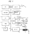
- Fig. 1 illustrates an embodiment 1 of the present invention, wherein following units are connected to a system bus 19.
- a central processing unit (CPU) 1 controls the functions of the entire apparatus, and also effects image editing operation according to a system program stored in a memory 2.
- a main memory 2 stores the system program to be executed by the CPU 1, and also contains an image memory for storing image data to be subjected to the image editing, and a work memory for storing various data related to the image processing.
- An input/output interface (I/O) 3 effects data transfer with external equipment.
- a video random access memory (RAM) 4 stores image data of an image frame to be displayed on a CRT (display unit) 5.
- the image data stored in the video RAM 4 are read by the CRT 5 and visually displayed.
- the image data stored in the video RAM 4 have a resolution of 100 dpi (dot/inch).
- a LAN (local area network) interface 7 effects data transfer with other image processing apparatus connected to the LAN.
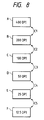
- a compression/expansion circuit 8 stepwise compresses the image data of 400 dpi, under the instruction of the CPU, thus generating compressed encoded image data of 12.5 dpi.
- Said compression/expansion circuit 8 effects the compression or expansion in the JBIG method.
- a direct memory access controller (DMAC) 15 is connected to a disk interface 9 and a scanner/printer interface 12 and effects reading/writing of the image data of input/output units (scanner 14, printer 13) and memory media (floppy disk 10, rigid disk 11) from or to a memory area, instructed by the CPU 1, in the main memory 2.
- DMAC direct memory access controller
- a key interface 16 transfers, to the CPU 1, the information entered from a keyboard 17 or a coordinate input device 18 called mouse.
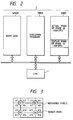
- Fig. 2 illustrates areas of the main memory 2 shown in Fig. 1.
- an image area IMEM for storing image data from the scanner 14; a program area PMEM for storing a program to be executed; and a work area WMEM for storing work data.
- the pixel data A1 - A16 of 4 x 4 pixels for example of 400 dpi are compressed to pixel data B1 - B4 of 200 dpi, and the differences of the compressed pixel data B1 - B4 and the original pixel data A1 - A16 are encoded.
- the compressed pixel data are considered as new pixel data A1 - A16 for compression and are subjected to compression and encoding.
- the compression is conducted in this manner to the image data of minimum resolution of about 12.5 dpi, which are used for communication or storage, together with the encoded data.
- the image data of minimum resolution (12.5 dpi) and the corresponding encoded data are utilized for preparing the image data of an upper rank (25 dpi). Subsequently image data of higher resolutions are prepared in succession, up to the original image data of 400 dpi.
- compressed data of a pixel is determined by entering the high resolution pixel data of A6 - A8, A10 - A12 and A14 - A16 surrounded by a thick line and the already compressed pixel data B1 - B3 into a weighting equation.
- the data employed for encoding are taken from the data of the reference pixels, but the positions and number of said reference pixels are made variable according to the contents of such reference around the target pixel to be encoded.
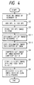
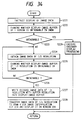
- Fig. 4 is a flow chart showing an example of the control program stored in the program area PMEM shown in Fig. 2.
- a step S1 an image, for example of a ship, is read by the scanner 14 of 400 dpi, and the obtained image information of 400 dpi is stored in the image area IMEM of the main memory 2. Said image information is converted to a lower resolution, by the compression/expansion circuit 8 according to the JBIG method, and the obtained image information of 100 dpi is stored in a buffer memory of the image area IMEM.
- a step S2 releases the image information of 100 dpi from the buffer memory to the system bus, and a step S3 stores said information in the VRAM 4.
- a step S3 stores said information in the VRAM 4.
- a step S3-1 an image clipping is instructed from the keyboard 17. It is assumed that the clipping of the entire read image of ship is instructed.
- a step S3-2 copies the image data (400 dpi), instructed for clipping, on the image area IMEM of the main memory 2.
- a step S4 compresses the clipped image data, prepared in the buffer of the image memory IMEM, by the compression/expansion circuit 8 according to the JBIG method, thereby obtaining a low resolution image of 12.5 dpi.
- a step S5 stores the image data of 12.5 dpi and the encoded data in the rigid disk 11, and stores the image data of 12.5 dpi in another buffer of the main memory 2.
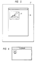
- a step S6 registers the image data stored in the buffer as an icon, then stores said image data in the VRAM 4 through the system bus, and displays a ship image of 12.5 dpi, reduced to a size of (1/16) x (1/16) of the original image, on a clipboard window on the image frame 21.
- Fig. 6 illustrates the icon displayed on the clipboard window.
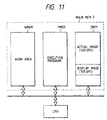
- Fig. 7 is a flow chart of an embodiment 2 of the present invention, indicating the process for image display with a resolution of 100 dpi on the CRT 6.
- a step S101 reads the image data of 400 dpi by the scanner 14, and stores the read image data of 400 dpi in the image memory IMEM of the main memory 2 (cf. Fig. 11). Then for hierarchical encoding by the JBIG method, a step S102 effects compressions of two steps in the JBIG method, thereby obtaining data C + C1 + C2, wherein C indicates the data of lower resolution (100 dpi) obtained by stepwise reduction of resolution in the JBIG method as shown in Fig. 8, and C1 and C2 indicate the encoded difference data.
- a next step S103 transfers said data C (100 dpi), stored in IMEM of the main memory, to the VRAM 4, and displays said data on the CRT.
- a next step S104 discriminates whether the hierarchical encoded data obtained in the JBIG method are to be registered as a file, and, if affirmative, a step S105 effects compressions of three steps to prepare data C3 + C4 + C5 + F (cf. Fig. 8).
- a step S106 stores the data C1 + C2 + C3 + C4 + C5 + F in the disk, and a step S107 effects the window display of data F as an icon as in the foregoing embodiment (in practice there is executed a process for pasting said icon on the clipboard).
- the present embodiment can transfer the image of 100 dpi, obtained in the stepwise encoding, to the VRAM for visual display.
- Fig. 9 shows a variation of this embodiment, in which the image data stored in the rigid disk 11 or the floppy disk 10 (namely low resolution data F of 12.5 dpi and encoded data C1 - C5: cf. Fig. 8) are read to the main memory 2 and are displayed on the CRT 5.
- the image data stored in the rigid disk 11 or the floppy disk 10 namely low resolution data F of 12.5 dpi and encoded data C1 - C5: cf. Fig. 8 are read to the main memory 2 and are displayed on the CRT 5.
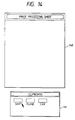
- a step S110 selects the data to be displayed. More specifically, one of the displayed icons is selected by the mouse. Then a step S111 displays an image processing sheet window on the CRT. Then a step S112 discriminates whether an undisplayed image is present, and, if affirmative, a step S113 acquires a display image buffer area on the image memory IMEM of the main memory 2.
- a next step S114 converts the data, read from the rigid disk or the floppy disk, to 100 dpi by the expansion circuit, and writes the expanded data in the display image buffer.
- a next step S115 transfers the image data of 100 dpi from the display image buffer to the VRAM, thereby displaying an image on the image processing sheet window.
- step S112 identifies that the undisplayed image is absent, the sequence proceeds to a step S116 for displaying other text data or vector data on the image processing sheet window.
- the present embodiment can directly store the data of 100 dpi in the display image buffer, utilizing the feature of the JBIG method of increasing the resolution in succession from the image data of lowest resolution (12.5 dpi), without the conventional procedure of once storing the image data of 400 dpi in the main memory 2 and converting said data to 100 dpi.
- Fig. 10 shows, as reference, the conventional technology corresponding to the embodiment shown in Fig. 9, and the comparison of Figs. 10 and 9 will clarify the feature of the present embodiment.
- a step S120 selects the data to be displayed, and a next step S121 displays an image processing sheet window on the CRT.
- a step S122 identifies the presence of an undisplayed image
- a step S123 discriminates whether a real image buffer (for 400 dpi) has been acquired on the main memory. If such buffer area has been acquired, a step S124 erases said real image buffer.
- a next step S125 acquires a real image buffer and a display image buffer area on the image memory IMEM of the main memory. Then a step S126 writes the image data (400 dpi) from the rigid disk or floppy disk, into the real image buffer.
- a step S127 prepares a display image (100 dpi) in the display image buffer, based on the image data (400 dpi) stored in the real image buffer.
- a next step S128 transfers the image data (100 dpi) from the display image buffer to the VRAM, thereby displaying an image in the image processing sheet window.
- a step S129 displays other text data or vector data on the image processing sheet window.
- the present embodiment utilizes the image data of 100 dpi, obtained in the course of expansion by the JBIG method, for display. Consequently, also in case of scroll display, there can be dispensed with the process of converting the data of 400 dpi to 100 dpi, according to a procedure shown in Fig. 12.
- a step S130 instructs the scrolling display.
- a next step S131 discriminates whether the scrolling area contains an image, and, if affirmative, a step S132 transfers the display image (100 dpi), expanded by the JBIG method, to the VRAM. Then a step S133 displays other text data or vector data in the scrolling area.
- An embodiment 3 provides a procedure for expanded display of an identification mark displayed in a part of the CRT (namely an icon pasted on the clipboard).
- Fig. 13 is a flow chart showing the control sequence of said embodiment 3, and Figs. 14 to 16 show the examples of display in a process of selecting an icon on the clipboard (said icon being displayed in reduced size with 12.5 dpi, as explained before) and fitting said icon on a desired edited position.
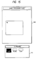
- a step S135 selects image data to be pasted. For example, a ship image (12.5 dpi) is selected from plural icons on the clipboard, as shown in Fig. 14. Then a step S136 designates the position of pasting on the image processing sheet window (cf. Fig. 15).
- a next step S137 acquires a pasting image buffer area in the image memory IMEM of the main memory 2.
- a next step S138 increases the resolution to 100 dpi by the compression/expansion circuit 8, based on the data (data of lowest resolution and encoded difference data) stored in the rigid disk, and writes said image data of 100 dpi in the pasted display image buffer.
- a last step S139 transfer the image data of 100 dpi from said buffer to the VRAM, for displaying a pasted image on the image processing sheet window (cf. Fig. 16).
- the present embodiment can directly display the data of 100 dpi obtained in the course of expansion of the icon of 12.5 dpi on the clipboard, and can therefore dispense with the process of converting the data of 400 dpi into data of 100 dpi for display. This feature will be more clearly understood from the comparison with a conventional technology shown in Fig. 17.
- a step S145 selects the image data to be pasted, then a step S146 designates the location of pasting on the image processing sheet window, and a step S147 acquires a real pasted image buffer area and a displayed image buffer area in the image memory IMEM of the main memory.
- a step S148 transfer the image data to be pasted, from the rigid disk, to said real pasted image buffer area.
- a next step S149 prepares, from the image data transferred to said real pasted image buffer, a display image in the display image buffer area.
- a last step S150 transfers the image data from said display image buffer to the VRAM, thereby displaying a pasted image on the image processing sheet window.
- An embodiment 4 of the present invention attains effective utilization of the image memory area IMEM of the main memory 2, thereby enabling to store a larger number of display images.
- Fig. 18 shows a general occupied state of the image buffer in the main memory.
- the image memory area IMEM is storing display images for displaying two images A, B on the CRT.
- Such state of the IMEM is obtained in the following manner.
- a first image A read by the scanner 14, is stored in the IMEM as a real image of 400 dpi, then said image is converted to a display image (100 dpi) for display on the CRT, and the converted data is stored in the IMEM, as the display image (100 dpi) for the image A.
- a second image B is read by the scanner 14, and the real image data of 400 dpi is overlaid in the area which stores the real image (400 dpi) of the image A, whereby the real image (400 dpi) of the image B is stored in the IMEM.
- a display image obtained by conversion to 100 dpi, is stored for the image B.
- the memory area may become deficient if a larger number of display image data (100 dpi) is to be stored.
- images of lower resolution are stored for display, instead of the resolution of 100 dpi for display.
- the present embodiment enables to store all the necessary image data in the IMEM, utilizing the formation of images of lower resolution by the hierarchical encoding of the JBIG method.
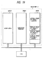
- Fig. 19 shows a state in which the image memory area IMEM of the main memory 2 stores the display image data (25 dpi) of three images A, B and C.
- Said display image data may be of a resolution of 50 dpi, or even of 12.5 dpi.
- the foregoing description is based on a principle of storing display image data prepared from the real image data read by the scanner, but it is also possible to expand the low resolution image data of 12.5 dpi and the encoded difference data, already stored in the disk, and to use thus expanded data for display.
- FIG. 20 shows a principal circuit structure for realizing the present embodiment
- Fig. 21 shows the display state of the present embodiment, in the high-speed page flipping mode
- Fig. 22 shows the image display state of the expanded image
- Fig. 23 shows the operation means of the present embodiment
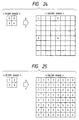
- Figs. 24 and 25 show specific examples of interpolation of the present embodiment.
- an image interpolation circuit 224 for expanding the size of reduced image serves to interpolate the reduced image data of 25 dpi as shown in Fig. 24 or 25, thereby expanding the size of the image, and to send the interpolated data to the CRT 5 through the VRAM 4. It is assumed that image data of plural images, obtained for example from the scanner 14, are already converted into reduced image data of 25 dpi and encoded data, by the image compression of the JBIG method shown in Fig. 8, and are already stored in the rigid disk 11 or the floppy disk 10.
- step S201 When high-speed image display (high-speed page flipping) is instructed for example from the keyboard 17 shown in Fig. 1 (step S201), the data to be displayed is selected (step S202), and an image processing sheet window 220 is displayed, as shown in Fig. 21, on the display image frame 221 of the CRT 5 (step S203). Then a display image buffer area of 25 dpi is acquired in the image memory area IMEM of the main memory 2 (step S205), and the image data to be displayed are transferred from the rigid disk 11 or the floppy disk 10 to said display image buffer (step S206).
- the above-mentioned reduced image data of 25 dpi separate from the encoded data, are stored in said display image buffer in the image memory area IMEM.
- the reduced image data are transferred, from said display image buffer, through the image interpolation circuit 224 to the VRAM 4, for image display on the image processing sheet window 220 on the CRT 5 (step S207).
- said image interpolation circuit 224 expands the reduced image data to the original image size, by a relatively simple interpolation such as zero value interpolation or same value interpolation as shown in Figs. 24 or 25, whereby images as shown in Fig. 21 are displayed in succession at a high speed, on the image processing sheet window 220.
- step S204 After the image data are all transferred from the display image buffer to the VRAM 4, the sequence returns to the step S204, and the above-mentioned steps S205 to S207 are repeated if an undisplayed image exists for example in the rigid disk 11. If such undisplayed image is absent, a step S208 effects necessary post-process and the sequence returns to the main program.
- step S209 If the high-speed image display is not instructed, there is executed normal image display by expanding the reduced image data of 12.5 dpi and the encoded data to the original image by the compression/expansion circuit 8 and displaying the expanded original image on the CRT 5 (step S209).
- the displayed image is as clear as the original image, as shown in Fig. 22.
- This embodiment enables high-speed image display in simple and rapid manner, and with a limited image memory, since the image expansion process is not involved in the high-speed image display.
- the image quality is inferior, as schematically illustrated in Fig. 21, to the ordinary display obtained by the expansion process, as shown in Fig. 22, but such image quality is not a problem in practice, because, in the high-speed page flipping mode, the user only needs to identify the displayed image.
- the reduced image data are assumed to be of 25 dpi, but there may be employed those of 12.5 dpi.
- Figs. 26 to 32 show an embodiment 6, which, in the clipping of image data, displays the stepwise reduced image data in succession and finally erases the display, thereby clearly informing the user of the proceeding of the clipping process.
- Fig. 26 shows the control sequence of the present embodiment
- Figs. 27 to 31 show examples of display
- Fig. 32 shows the control sequence of a variation of the present embodiment.
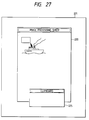
- Fig. 27 an image shown in Fig. 27 is displayed on the image processing sheet window 220 of the display frame 221 of the CRT 5.
- a clipboard window 225 is displayed on the display frame 221 (step S211).
- the user designates the clipping area for example with a mouse, as indicated by a pointer P shown in Figs. 27 and 28, and, when the clipping area designation is completed as shown in Fig. 28 (step S213), the CPU 1 acquires a clipping image data buffer area in the image memory area IMEM of the main memory 2 (step S214).
- step S216 the data in said clipping image data buffer are compressed and encoded by the compression/expansion circuit 8 according to the JBIG method shown in Fig. 8, thereby initially obtaining the reduced image data (200 dpi) and encoded data of a first stage (step S216).
- Said reduced image data are written by overlay into the clipping image data buffer, and are also transferred to the VRAM 4 for display on the CRT 5.
- image data with a resolution of 1/2 are displayed on the image processing sheet window 220 (step S217).
- the above-explained steps S216 and S217 are repeated until the completion of the stepwise encoding.
- the image resolution varies in the steps of 400 dpi, 200 dpi, 100 dpi, 50 dpi, 25 dpi and 12.5 dpi, and the image size is also reduced to 1/4 with a reduction of 1/2 in the resolution. Consequently the image for clipping (a ship image in this case) displayed on the image processing sheet window 220 is reduced in size, as shown in Figs. 28, 29 and 30, corresponding to the process stage of the compression encoding, so that the user can clearly understand the progress of the clipping process.
- step S228 When the encoding is completed (step S218), the final reduced data are stored in the clipboard, then the image on the image processing sheet window 220 is erased as shown in Fig. 31, and the clipped reduced image of 12.5 dpi is pasted as an icon, on the clipboard window 225 through the VRAM 4 (step S219). Thereafter the control sequence returns to the main flow. Thus the user can immediately know the completion of the clipping procedure.
- the image to be clipped remains displayed in its original size for several seconds to about twenty seconds until the completion of the clipping procedure, and said image is suddenly erased upon said completion. Consequently the user is unable to comprehend the progress of the clipping procedure and finds difficulty in maintaining the work.
- the present embodiment displays the reduced images in succession in smaller sizes, and the above-mentioned inconvenience can therefore be resolved.
- Fig. 32 shows the control sequence of a variation of the embodiment 6, and the difference of said variation lies in a fact that, in a step S220 next to the step S216, an image of a resolution of 1/2 is displayed on the image processing sheet window 220 through the image interpolation circuit 224 as shown in Fig. 20. Consequently, in said variation, the displayed image, instead of being reduced in size as shown in Figs. 29 and 30, remains same in size as shown in Fig. 21 but becomes stepwise thinner and vanishes at the completion of encoding (step S219). It will be apparent that this variation provides the same effect as in the foregoing embodiment.
- Figs. 33 to 37 show an embodiment 7 of the present invention.
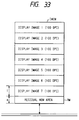
- the capacity a of the residual memory area RM of the display image buffer acquired in the image memory IMEM of the main memory 2 becomes smaller than an image frame capacity T as shown in Fig. 33, the display of at least another image is rendered possible, thereby achieving effective utilization of the memory and improvement in the work efficiency.
- step S221 When an instruction for the image data display is given from the keyboard 17 (step S221), there is discriminated whether the display image buffer of an image frame can be acquired in the display image buffer area of the image memory IMEM (step S222), by comparing the capacity a of the above-mentioned residual memory area RM with a capacity T required for an image frame.
- step S223 If a ⁇ T, indicating that said display image buffer can be acquired (step S223), there is executed the ordinary image display process of storing the display image data of a new image frame of 100 dpi in said display image buffer and displaying said data on the CRT 5 through the VRAM 4 (step S229), and then the sequence returns to the main routine.
- the sequence proceeds to a step S224 for obtaining an image with a resolution of 1/2.
- the reduced image data of 12.5 dpi and the encoded data of the JBIG method are supplied from the rigid disk 11 or the floppy disk 10 to the compression/expansion circuit 8 and are subjected to the JBIG expansion to obtain reduced image data of 50 dpi (step S224).
- the capacity b required for the reduced image data of 50 dpi is compared with the capacity a of the residual area RM, and said acquisition is identified possible or impossible respectively if b ⁇ a or b > a.
- step S226) If said acquisition is identified impossible (step S226), the above-mentioned steps S224 and S225 are repeated until said acquisition becomes possible. More specifically, in a second cycle, reduced image data of 25 dpi are prepared in the compression/expansion circuit 8, then the capacity c required for said reduced image data (cf. Fig. 35) is compared with the capacity a of the residual memory area RM, and said acquisition is identified possible or impossible respectively if c ⁇ a or c > a.
- the sequence proceeds from the step S226 to S227 for transferring, to said display image buffer, the image data of a resolution of 1/n, decoded to the resolution level of the buffer (for example reduced image data of 25 dpi).
- said image data of resolution of 1/n are read from the display image buffer, enlarged to the original image size through the image interpolation circuit 224 shown in Fig. 20, and transferred to the VRAM 4, thereby displaying the image of the resolution of 1/n on the image processing sheet window 220 (cf. Fig. 22) on the CRT 5 (step S228).
- the interpolation in this state is executed as shown in Fig. 24 or 25, whereby the display is made with somewhat deteriorated image quality, as shown in Fig. 21. Subsequently the sequence returns to the main program.
- Such display is considered practically acceptable, since some deterioration in the image quality is not a problem for merely confirming the content of image.
- the present embodiment provides an advantage of constantly enabling to see the entire image.
- Figs. 36 and 37 show a variation of the embodiment 7.
- the image data of an image frame are usually divided into m stripes at maximum, satisfying a condition d x m ⁇ T, and the JBIG compression is executed for each stripe, and the reduced image data of 12.5 dpi and the encoded data are stored in the rigid disk 11 or the floppy disk 10.
- the present embodiment is to display image data of an image frame, utilizing the combination of m stripes at maximum according to the capacity a of the residual memory area RM, without reducing the resolution from 100 dpi.
- Step S231 - S233 and S239 will not be explained as they are similar to the steps S221 - S223 and S229 in Fig. 34.
- a step S234 obtains image data of 100 dpi, which are less by one stripe than in the preceding cycle, by the compression/expansion circuit 8, based on the data from the rigid disk 11 etc.
- a step S235 discriminates whether a display image buffer, for said data reduced by one stripe, can be acquired on the image memory area IMEM.
- step S236 If the acquisition is identified impossible (step S236), the above-mentioned steps S234 and S235 are repeated until said acquisition becomes possible.
- step S236 When the step S236 subsequently identifies that the acquisition is possible, the composite image data are stored in the display image buffer by an amount corresponding to the acquired stripes (step S237), and said image data in the display image buffer are displayed in the original stripe position, on the image processing sheet window 220 (cf. Fig. 22) on the CRT 5 (step S238). Subsequently the sequence returns to the main routine.
- the order of selection of stripes in the step S234 can be variously considered according to the nature of the image. For example, if important image information is concentrated in the upper part of the image frame (for example a control chart), the stripes may be discarded from the lower part of the image frame. In case the important image information is concentrated in the center of the image frame (for example a design chart), the stripes may be discarded alternately from the upper and lower parts so as to leave the central stripes to the last. Consequently the image displayed on the CRT 5 in the step S238 shows the important image portions by a combination of stripes.
- the present embodiment provides an advantage of displaying the image with a resolution of 100 dpi which is same as the resolution of the CRT 5, and the present embodiment does not require the image interpolation circuit 224.
- the above-explained embodiment repeats the steps S224 and S225 (or steps S234 and S235) until the display image buffer is acquired, but it is also possible to determine, in one operation, the resolution of 1/n (or number i of stripes) through the comparison of the capacity a of the residual memory area RM with a predetermined capacity e i for each resolution (or comparison of the capacity a with n x i).
- step S228 in Fig. 34 displays the image through the image interpolation circuit 224, but it is also possible to automatically decide the display according to the resolution, for example to display the image data of 100 dpi expanded by the compression/expansion circuit 8 in case of a very low resolution, and to effect the display without image interpolation in case the resolution is relatively high.
- the present embodiment enables image display even in case of capacity deficiency of the display image buffer area, thereby improving the operating efficiency.
- the original image data (400 dpi) stored in the main memory 2 (Fig. 38) are divided into horizontally oblong plural stripes (areas) arranged in the vertical direction, and said original image data are hierarchically encoded by the compression/expansion circuit 8 for each stripe in the main memory 2.
- a comparator 301 Based on the data in a stage in the course of said encoding, a comparator 301 effects a comparison:
- Fig. 41 shows the different process stages for the stripes, attained through the above-explained procedure. The process is completed at the 4th stage for the stripe 1, 2nd stage for the stripe 2, and 3rd stage for the stripe 3.
- the image data (100 dpi), displayed on the CRT 5 and stored in the image memory IMEM of the main memory 2, are divided into plural stripes, as in the embodiment 8. Then, when a clipping procedure to the clipboard is initiated as shown in Fig. 42, a step S311 awaits the designation of the clipping area utilizing the image displayed on the CRT 5, and a step S312 identifies a stripe to which the image A of the designated clipping area belongs (stripe 2 in Fig. 43). Based on the result of said identification, a step S313 effects stepwise encoding on the image data (100 dpi) of the corresponding stripe in the image memory IMEM for example to a resolution of 12.5 dpi.
- a step S314 discriminates whether the encoding has been completed for all the stripes to which the image A belongs (in case of Fig. 43, the image A belongs only to the stripe 2, but it may belong to plural stripes), and the step S313 is repeated until the encoding is completed.
- a step S315 writes, with respect to all the encoded stripe data to which the image A belongs, a header (consisting of the position of the encoded stripe in the image data on the image memory IMEM, position (X, Y) of the image A in the stripe, and image data size (width W and height H), and the encoded data (containing image data of 12.5 dpi of corresponding stripe) in a predetermined area of the clipboard of the image memory IMEM in the main memory 2.
- Such operating mode reduces the write-in data capacity into the clipboard, thereby achieving efficient utilization of the memory.
- a step S318 decodes (100 dpi) the data of all the stripes to which the image A belongs, stored in the predetermined area of the clipboard of the image memory IMEM in the main memory 2, and stores the decoded data in the image memory IMEM, then a step S319 extracts the actually pasted image A from the image data of 100 dpi of the decoded stripes in the image memory IMEM based on the header information in the predetermined area of said clipboard and stores said image A in the buffer acquired in the step S317, and a step S320 displays the image A, extracted from said buffer, in the pasting position on the CRT 5, according to the designating information in the step S316.
- This procedure utilizes only the data of the necessary stripes, thereby achieving efficient utilization of the memory.
- a system shown in Fig. 46 includes a work station WS4 functioning as a server of the structure shown in Fig. 1; work stations WS1, WS3 lacking the printer and the rigid disk; and a work station WS2 provided with a rigid disk llA.
- Each of the work stations WS1 - WS3 is equipped with the CRT 5, VRAM 4, CPU 1, main memory 2, I/O 3, LAN interface 7, compression/expansion circuit 8, key interface 16, keyboard 17 and mouse 19.
- a number 6 indicates the local area network (LAN).
- the disk 11 of the work station WS4 stores the image data C + C1 + C2 (Fig. 8).
- the work station WS1 can display the image C on the CRT, and can effect editing operation by the mouse or the keyboard.
- the edited content H is stored in the main memory of the work station WS1.
- the edited content H alone is transferred from the main memory of WS1 to that of WS4 through the LAN 6, then the image data A are decoded in the WS4 from the data C + C1 + C2 stored in the disk 11, then the edited data H are added thereto, and the edited image data A' are printed in the printer 13. Also in case of storing said image data A', said data A' are stepwise encoded to obtain C' + C1' (corresponding to C1) + C2' (corresponding to C2), which are then stored in the disk 11.
Applications Claiming Priority (3)
| Application Number | Priority Date | Filing Date | Title |
|---|---|---|---|
| JP04384592A JP3226588B2 (ja) | 1992-02-28 | 1992-02-28 | 画像処理装置、システムおよび方法 |
| JP43845/92 | 1992-02-28 | ||
| JP4384592 | 1992-02-28 |
Publications (2)
| Publication Number | Publication Date |
|---|---|
| EP0559376A1 EP0559376A1 (en) | 1993-09-08 |
| EP0559376B1 true EP0559376B1 (en) | 1999-06-16 |
Family
ID=12675071
Family Applications (1)
| Application Number | Title | Priority Date | Filing Date |
|---|---|---|---|
| EP93301402A Expired - Lifetime EP0559376B1 (en) | 1992-02-28 | 1993-02-25 | Image processing apparatus |
Country Status (4)
| Country | Link |
|---|---|
| US (1) | US5657477A (ja) |
| EP (1) | EP0559376B1 (ja) |
| JP (1) | JP3226588B2 (ja) |
| DE (1) | DE69325297T2 (ja) |
Families Citing this family (15)
| Publication number | Priority date | Publication date | Assignee | Title |
|---|---|---|---|---|
| US6021259A (en) * | 1995-07-10 | 2000-02-01 | International Business Machines Corporation | Apparatus and method for conversion of structured data between different formats |
| JP3634556B2 (ja) | 1997-05-12 | 2005-03-30 | キヤノン株式会社 | 画像処理方法及びそのシステム |
| US7315386B1 (en) | 1997-06-30 | 2008-01-01 | Fujifilm Corporation | Image communication system and method |
| US6411395B1 (en) * | 1997-07-23 | 2002-06-25 | International Business Machines Corporation | Apparatus and method for conversion of data between different formats |
| US6441927B1 (en) | 1998-08-07 | 2002-08-27 | Hewlett-Packard Company | Appliance and method for viewing captured images |
| US7042583B1 (en) | 1999-04-12 | 2006-05-09 | Eastman Kodak Company | Techniques for acquiring a parent multimedia asset (digital negative) from any of a plurality of multiply modified child multimedia assets |
| WO2000062539A1 (en) * | 1999-04-12 | 2000-10-19 | Pictureiq Corporation | Acquiring a multimedia asset from any of a plurality of multiply modified child multimedia assets |
| JP3478329B2 (ja) * | 1999-10-01 | 2003-12-15 | セイコーエプソン株式会社 | 画像処理装置及び画像処理方法 |
| US7460157B2 (en) | 2000-02-02 | 2008-12-02 | Fujifilm Corporation | Image storing-transferring method and apparatus, image processing method, image processing system, and image processor |
| KR100386036B1 (ko) * | 2000-06-27 | 2003-06-02 | (주)버추얼미디어 | 티씨피/아이피 네트워크 상에서의 디지털 비디오편집시스템 및 그 제어방법 |
| JP4173709B2 (ja) | 2002-09-26 | 2008-10-29 | 富士フイルム株式会社 | データ管理方法およびデータ管理装置並びにプログラム |
| US7447369B2 (en) * | 2003-03-07 | 2008-11-04 | Ricoh Co., Ltd. | Communication of compressed digital images |
| US20050052688A1 (en) * | 2003-08-12 | 2005-03-10 | Teruyuki Maruyama | Document edit method and image processing apparatus |
| JP2010072092A (ja) * | 2008-09-16 | 2010-04-02 | Sanyo Electric Co Ltd | 画像表示装置及び撮像装置 |
| US9889080B2 (en) | 2015-05-07 | 2018-02-13 | Celeb LLC | Color depositing shampoo |
Family Cites Families (12)
| Publication number | Priority date | Publication date | Assignee | Title |
|---|---|---|---|---|
| JPS5911063A (ja) * | 1982-07-12 | 1984-01-20 | Ricoh Co Ltd | フアクシミリ装置 |
| US4675908A (en) * | 1983-10-07 | 1987-06-23 | Canon Kabushiki Kaisha | Image data processing apparatus and system |
| JPS6085680A (ja) * | 1983-10-17 | 1985-05-15 | Canon Inc | 画像処理方法 |
| US4742558A (en) * | 1984-02-14 | 1988-05-03 | Nippon Telegraph & Telephone Public Corporation | Image information retrieval/display apparatus |
| EP0381299B1 (en) * | 1984-11-14 | 1998-08-12 | Canon Kabushiki Kaisha | Image processing system |
| JPH0824336B2 (ja) * | 1986-05-30 | 1996-03-06 | 株式会社東芝 | 画像情報処理装置 |
| US5138702A (en) * | 1987-04-17 | 1992-08-11 | Minolta Camera Co., Ltd. | External image input/output device connectable image processing system |
| US4837635A (en) * | 1988-01-22 | 1989-06-06 | Hewlett-Packard Company | A scanning system in which a portion of a preview scan image of a picture displaced on a screen is selected and a corresponding portion of the picture is scanned in a final scan |
| US4870497A (en) * | 1988-01-22 | 1989-09-26 | American Telephone And Telegraph Company | Progressive transmission of high resolution two-tone facsimile images |
| KR900702449A (ko) * | 1988-06-20 | 1990-12-07 | 야마모도 다꾸마 | 멀티윈도우 통신 시스템(Multi-Window Communication System) |
| JP2756301B2 (ja) * | 1989-04-10 | 1998-05-25 | キヤノン株式会社 | 画像編集方法及び装置 |
| US4979049A (en) * | 1989-06-01 | 1990-12-18 | At&T Bell Laboratories | Efficient encoding/decoding in the decomposition and recomposition of a high resolution image utilizing its low resolution replica |
-
1992
- 1992-02-28 JP JP04384592A patent/JP3226588B2/ja not_active Expired - Fee Related
-
1993
- 1993-02-24 US US08/021,858 patent/US5657477A/en not_active Expired - Lifetime
- 1993-02-25 DE DE69325297T patent/DE69325297T2/de not_active Expired - Lifetime
- 1993-02-25 EP EP93301402A patent/EP0559376B1/en not_active Expired - Lifetime
Also Published As
| Publication number | Publication date |
|---|---|
| DE69325297D1 (de) | 1999-07-22 |
| DE69325297T2 (de) | 1999-11-25 |
| US5657477A (en) | 1997-08-12 |
| EP0559376A1 (en) | 1993-09-08 |
| JP3226588B2 (ja) | 2001-11-05 |
| JPH05244437A (ja) | 1993-09-21 |
Similar Documents
| Publication | Publication Date | Title |
|---|---|---|
| EP0558313B1 (en) | Image processing apparatus | |
| EP0559376B1 (en) | Image processing apparatus | |
| US20030095596A1 (en) | Image processing apparatus, image processing method, and a computer-readable storage medium containing a computer program for image processing recorded thereon | |
| EP0572228B1 (en) | Data processing method and apparatus therefor | |
| JP2006333495A (ja) | 画像処理方法、文書表示方法及びコンピュータ実行操作選択方法 | |
| JPH06245056A (ja) | 画像データの拡大・平滑化処理装置 | |
| US20040131262A1 (en) | Image processing device, image forming apparatus, program, and storing medium | |
| US5862412A (en) | Apparatus for converting document data into bit map data and compressing display image formed by combining the bit map data and image data | |
| US6232978B1 (en) | Image processing apparatus, and method of controlling same, using a combination of enlargement and fixed ratio reduction processing | |
| JP3081051B2 (ja) | 画像処理装置および画像処理方法 | |
| JPH05241537A (ja) | 画像処理装置 | |
| JP3160349B2 (ja) | 画像処理装置および方法 | |
| US5438432A (en) | Data transmitting apparatus | |
| JP3346051B2 (ja) | 画像処理装置 | |
| JP4360021B2 (ja) | 画像処理装置および画像処理方法 | |
| US20020101606A1 (en) | Fast preview of CCITT-compressed documents | |
| JPH09198017A (ja) | 圧縮画像の縮小・拡大方法及びその装置 | |
| JP2899263B2 (ja) | コンピュータの制御方法 | |
| JP2812389B2 (ja) | 文書通信装置 | |
| JP3190085B2 (ja) | 画像処理装置及び方法 | |
| JP3471925B2 (ja) | 複写装置及び画像処理方法 | |
| JPS6359674A (ja) | 画像処理方法 | |
| JPH05258067A (ja) | 圧縮されたイメージを復号する方法 | |
| JPH08125848A (ja) | 画像処理装置 | |
| JPH07234928A (ja) | イメージデータ管理方法 |
Legal Events
| Date | Code | Title | Description |
|---|---|---|---|
| PUAI | Public reference made under article 153(3) epc to a published international application that has entered the european phase |
Free format text: ORIGINAL CODE: 0009012 |
|
| AK | Designated contracting states |
Kind code of ref document: A1 Designated state(s): DE FR GB IT NL |
|
| 17P | Request for examination filed |
Effective date: 19940124 |
|
| 17Q | First examination report despatched |
Effective date: 19951205 |
|
| GRAG | Despatch of communication of intention to grant |
Free format text: ORIGINAL CODE: EPIDOS AGRA |
|
| GRAG | Despatch of communication of intention to grant |
Free format text: ORIGINAL CODE: EPIDOS AGRA |
|
| GRAH | Despatch of communication of intention to grant a patent |
Free format text: ORIGINAL CODE: EPIDOS IGRA |
|
| GRAH | Despatch of communication of intention to grant a patent |
Free format text: ORIGINAL CODE: EPIDOS IGRA |
|
| GRAH | Despatch of communication of intention to grant a patent |
Free format text: ORIGINAL CODE: EPIDOS IGRA |
|
| GRAA | (expected) grant |
Free format text: ORIGINAL CODE: 0009210 |
|
| AK | Designated contracting states |
Kind code of ref document: B1 Designated state(s): DE FR GB IT NL |
|
| REF | Corresponds to: |
Ref document number: 69325297 Country of ref document: DE Date of ref document: 19990722 |
|
| ET | Fr: translation filed | ||
| ITF | It: translation for a ep patent filed |
Owner name: SOCIETA' ITALIANA BREVETTI S.P.A. |
|
| PLBE | No opposition filed within time limit |
Free format text: ORIGINAL CODE: 0009261 |
|
| STAA | Information on the status of an ep patent application or granted ep patent |
Free format text: STATUS: NO OPPOSITION FILED WITHIN TIME LIMIT |
|
| 26N | No opposition filed | ||
| REG | Reference to a national code |
Ref country code: GB Ref legal event code: IF02 |
|
| PGFP | Annual fee paid to national office [announced via postgrant information from national office to epo] |
Ref country code: NL Payment date: 20090217 Year of fee payment: 17 |
|
| PGFP | Annual fee paid to national office [announced via postgrant information from national office to epo] |
Ref country code: IT Payment date: 20090205 Year of fee payment: 17 |
|
| PGFP | Annual fee paid to national office [announced via postgrant information from national office to epo] |
Ref country code: FR Payment date: 20090223 Year of fee payment: 17 |
|
| REG | Reference to a national code |
Ref country code: NL Ref legal event code: V1 Effective date: 20100901 |
|
| REG | Reference to a national code |
Ref country code: FR Ref legal event code: ST Effective date: 20101029 |
|
| PG25 | Lapsed in a contracting state [announced via postgrant information from national office to epo] |
Ref country code: NL Free format text: LAPSE BECAUSE OF NON-PAYMENT OF DUE FEES Effective date: 20100901 Ref country code: FR Free format text: LAPSE BECAUSE OF NON-PAYMENT OF DUE FEES Effective date: 20100301 |
|
| PG25 | Lapsed in a contracting state [announced via postgrant information from national office to epo] |
Ref country code: IT Free format text: LAPSE BECAUSE OF NON-PAYMENT OF DUE FEES Effective date: 20100225 |
|
| PGFP | Annual fee paid to national office [announced via postgrant information from national office to epo] |
Ref country code: DE Payment date: 20110228 Year of fee payment: 19 |
|
| PGFP | Annual fee paid to national office [announced via postgrant information from national office to epo] |
Ref country code: GB Payment date: 20110224 Year of fee payment: 19 |
|
| GBPC | Gb: european patent ceased through non-payment of renewal fee |
Effective date: 20120225 |
|
| REG | Reference to a national code |
Ref country code: DE Ref legal event code: R119 Ref document number: 69325297 Country of ref document: DE Effective date: 20120901 |
|
| PG25 | Lapsed in a contracting state [announced via postgrant information from national office to epo] |
Ref country code: GB Free format text: LAPSE BECAUSE OF NON-PAYMENT OF DUE FEES Effective date: 20120225 |
|
| PG25 | Lapsed in a contracting state [announced via postgrant information from national office to epo] |
Ref country code: DE Free format text: LAPSE BECAUSE OF NON-PAYMENT OF DUE FEES Effective date: 20120901 |