EP0529338B1 - Photomaske und Verfahren zur Herstellung - Google Patents
Photomaske und Verfahren zur Herstellung Download PDFInfo
- Publication number
- EP0529338B1 EP0529338B1 EP92113030A EP92113030A EP0529338B1 EP 0529338 B1 EP0529338 B1 EP 0529338B1 EP 92113030 A EP92113030 A EP 92113030A EP 92113030 A EP92113030 A EP 92113030A EP 0529338 B1 EP0529338 B1 EP 0529338B1
- Authority
- EP
- European Patent Office
- Prior art keywords
- phase shifter
- area
- phase
- light
- areas
- Prior art date
- Legal status (The legal status is an assumption and is not a legal conclusion. Google has not performed a legal analysis and makes no representation as to the accuracy of the status listed.)
- Expired - Lifetime
Links
Images


Classifications
-
- G—PHYSICS
- G03—PHOTOGRAPHY; CINEMATOGRAPHY; ANALOGOUS TECHNIQUES USING WAVES OTHER THAN OPTICAL WAVES; ELECTROGRAPHY; HOLOGRAPHY
- G03F—PHOTOMECHANICAL PRODUCTION OF TEXTURED OR PATTERNED SURFACES, e.g. FOR PRINTING, FOR PROCESSING OF SEMICONDUCTOR DEVICES; MATERIALS THEREFOR; ORIGINALS THEREFOR; APPARATUS SPECIALLY ADAPTED THEREFOR
- G03F1/00—Originals for photomechanical production of textured or patterned surfaces, e.g., masks, photo-masks, reticles; Mask blanks or pellicles therefor; Containers specially adapted therefor; Preparation thereof
- G03F1/26—Phase shift masks [PSM]; PSM blanks; Preparation thereof
- G03F1/30—Alternating PSM, e.g. Levenson-Shibuya PSM; Preparation thereof
-
- G—PHYSICS
- G03—PHOTOGRAPHY; CINEMATOGRAPHY; ANALOGOUS TECHNIQUES USING WAVES OTHER THAN OPTICAL WAVES; ELECTROGRAPHY; HOLOGRAPHY
- G03F—PHOTOMECHANICAL PRODUCTION OF TEXTURED OR PATTERNED SURFACES, e.g. FOR PRINTING, FOR PROCESSING OF SEMICONDUCTOR DEVICES; MATERIALS THEREFOR; ORIGINALS THEREFOR; APPARATUS SPECIALLY ADAPTED THEREFOR
- G03F1/00—Originals for photomechanical production of textured or patterned surfaces, e.g., masks, photo-masks, reticles; Mask blanks or pellicles therefor; Containers specially adapted therefor; Preparation thereof
- G03F1/68—Preparation processes not covered by groups G03F1/20 - G03F1/50
- G03F1/80—Etching
-
- G—PHYSICS
- G03—PHOTOGRAPHY; CINEMATOGRAPHY; ANALOGOUS TECHNIQUES USING WAVES OTHER THAN OPTICAL WAVES; ELECTROGRAPHY; HOLOGRAPHY
- G03F—PHOTOMECHANICAL PRODUCTION OF TEXTURED OR PATTERNED SURFACES, e.g. FOR PRINTING, FOR PROCESSING OF SEMICONDUCTOR DEVICES; MATERIALS THEREFOR; ORIGINALS THEREFOR; APPARATUS SPECIALLY ADAPTED THEREFOR
- G03F1/00—Originals for photomechanical production of textured or patterned surfaces, e.g., masks, photo-masks, reticles; Mask blanks or pellicles therefor; Containers specially adapted therefor; Preparation thereof
- G03F1/26—Phase shift masks [PSM]; PSM blanks; Preparation thereof
- G03F1/28—Phase shift masks [PSM]; PSM blanks; Preparation thereof with three or more diverse phases on the same PSM; Preparation thereof
Definitions
- the present invention relates to a photomask for use in optical lithography for the fabrication of semiconductor devices and so on, particularly to a photomask having phase shifters for shifting the phase of transmitted light, and to a method of fabricating the photomask.
- phase shift masks using phase shifters for shifting phases of transmitted light.
- a phase shift mask of e.g., a line and space pattern of alternated light shielding and light transmitting areas is intended to improve resolutions of patterns by setting at 180° a phase difference between light transmitting areas with light shielding areas therebetween.
- phase shift mask has a part in a light transmitting area, where a phase inversion of transmitted light takes place, i.e., an area (0° area) with no phase shifter formed thereon and an area (180° area) with a 180° phase shifter formed thereon are adjacent to each other, the intensity of the transmitted light is lowered at the part although the part is the light transmitting area. Consequently, by using such phase shift mask, resists adversely remain at parts where patterns are not to be formed. Attention has to be paid to arrangements of phase shifters so as not to form parts in light transmitting areas, where no phase inversions take place.
- a 90° shifter for example, is arranged at a part where a phase is inverted, whereby a sharp shift of a phase in a light transmitting area has been prevented.
- FIG. 12A is a plan view of the photomask
- FIG. 12B is a sectional view along the line A-A' of FIG. 12A
- FIG. 12C is a sectional view along the line B-B' of FIG. 12A.
- Chrome layers 102 are formed in lines on a mask substrate 100.
- phase shifters 104, 106 each for shifting a phase by 90° are superposed on each other, and the lower phase shifter 104 alone is formed on borders of the light transmitting areas with no phase shifter formed thereon.
- the borders of the light transmitting area without the phase shifters a phase is bluntly shifted by 90°, so that no sharp phase shifts takes place.
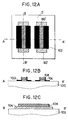
- FIG. 13A is a plan view of the photomask
- FIG. 13B is a sectional view along the line A-A' of FIG. 13A.
- chrome layers 102 are formed on a mask substrate 100, and 90° phase sifters 108 for shifting a phase by 90° and 270° phase shifters 110 for shifting a phase by 270° are alternately formed on each of light transmitting areas sandwiched by the chrome layers 102,.
- a phase is inverted in the boundary parts between the 90° phase shifter 108 and the 270° phase shifter 110. But in FIG. 13, because of the chrome layers 102 on the boundary parts, the light transmitting area has no parts where a phase inversion takes place.
- the conventional shift mask of FIG. 13 has the problem that a light intensity is so lowered in the boundary parts of the phase shifters 108, 110 that a focus margin upon an exposure is lowered.
- An object of the present invention is to provide a photomask and a method of fabricating the photomask, which can shift a phase in light transmitting areas without lowering the intensity of transmitted light, can easily correct defects of its phase shifters, and can secure a sufficient focus margin upon an exposure.
- the photomask may be fabricated using the method of claim 7.
- the first area with a 90° shifter formed on, and the second area with a 270° shifter formed on are arranged with a light shielding area or the third area with no phase shifter formed thereon located between the first and second areas. Consequently the photomask has no parts in the light transmitting area, where a phase of the transmitted light is sharply shifted, and consequently an intensity of the light is lowered. Furthermore, the 90° shifter and the 270° shifter are not overlapped on each other. Consequently even if a defect should take place in the 90° shifter or in the 270° shifter , the shifter could be easily corrected.
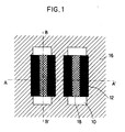
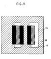
- Fig. 1 is a plan view of the photomask
- Fig. 2A is a sectional view along the line A-A' of Fig. 1
- Fig. 2B is a sectional view along the line B-B' of Fig. 1.
- chrome lines 12 of a light shielding layer are formed on a mask substrate 10 of quartz.
- An etching stopping layer 14 for blocking etching is formed on the entire mask substrate 10 including the chrome layers 12.
- the etching stopping layer 14 is formed of, e.g. Al 2 O 3 .
- the 90° phase shifter 16 is e. g. an about 190 nm-thickness SiO 2 layer. This 90° phase shifter 16 is formed uninterruptedly up to the peripheral areas of the chrome lines 12.
- a 270° phase shifter 18 for shifting a phase by 270° is formed on each of the right and the left light transmitting areas of the three light transmitting areas sandwiched by each of the four chrome lines 12 and its adjacent one.
- the 270° phase shifters 18 are formed of e. g. an about 570 nm-thickness SiO 2 layer.
- the 270° phase shifters 18 are formed only on the light transmitting areas between the chrome lines 12.
- the 90° phase shifter 16 is separated from the shorter sides of each of the 270° phase shifters 18 by light transmitting areas without any phase shifter formed thereon.
- the 90° phase shifter 16 is also separated from the longer sides of each of the 270° phase shifters 18 by the light shielding areas of the chrome lines 12.
- the 90° phase shifter 16 and the 270° phase shifter 18 are separated from each other by the light transmitting areas without any phase shifter formed them or by the light shielding areas of the chrome lines 12, and accordingly there is no part where a phase sharply shifts by an angle larger than 90°. Furthermore, the 90° phase shifter 16 and the 270° phase shifter 18 are not overlapped on each other, and consequently possible defects of the 90° phase shifter 16 and the 270° phase shifter can be corrected separately.
- a light intensity is not lowered in the outer boundary part of the phase shifters, and consequently a sufficient focus margin can be secured upon an exposure.
- a minimum light intensity obtained when a focal point is shifted was calculated on the photomask according to this embodiment of FIGs. 1 and 2, and the conventional photomask of FIG. 13.
- a light intensity is most lowered in the areas near the boundaries of the phase shifters 18.
- a light intensity is most lowered in the areas, which are boundary parts of the phase shifters 108, 110.
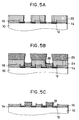
- a chrome layer 12 is evaporated on the entire surface of a mask substrate 10 of quartz and is patterned in lines. Subsequently on the entire surface an etching stopping layer 14 of Al 2 O 3 is evaporated. Then an about 190 nm-thickness SiO 2 layer 20 is evaporated on the entire surface (FIG. 4A).
- the SiO 2 layer 20 is etched by, e.g., RIE (Reactive Ion Etching) with the resist layer 22 as the mask, and the 90° phase shifter 16 is formed (FIG. 4C). This etching of the SiO 2 layer 20 is stopped at the etching stopping layer 14 and the surface of the mask substrate 10 is never etched.
- RIE Reactive Ion Etching
- SiO 2 layer 26 is evaporated on the entire surface (FIG 5B). The SiO 2 layer 26 is formed both on the etching stopping layer 14 and on the resist layer 24.
- the resist layer 24 is removed to lift off the resist layer 24 on the SiO 2 layer 26, and the 270° phase shifter 18 is formed (FIG. 5C).
- the 90° phase shifter 16 is formed by etching technique, and the 270° phase shifter 18 is formed by lift-off technique.
- a chrome layer 12 is evaporated on the entire surface of a mask substrate 10 of quartz, and is patterned in lines. Then an Al 2 O 3 etching stopping layer 14 is evaporated on the entire surface (FIG. 6A).
- an about 190 nm-thickness SiO 2 layer 30 is evaporated on the entire surface (FIG. 6C).
- the SiO 2 layer 28 is formed both on the etching stopping layer 14 and on the resist layer 28.
- the resist layer 28 is removed to lift off the SiO 2 layer 30 on the resist layer 28, and the 90° phase shifter 16 is formed (FIG. 6D).
- a resist layer 24 which is so patterned that a region for the 270° phase shifter to be formed is opened is formed (FIG. 7A), and an about 570 nm-thickness SiO 2 layer 26 is evaporated on the entire surface (FIG. 7B).
- the SiO 2 layer 26 on the resist layer 24 is lifted off, and the 270° phase shifter 18 is formed (FIG. 7C).
- both the 90° phase shifter 16 and the 270° phase shifter 18 are formed by lift-off technique.
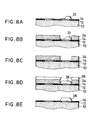
- a resist layer 34 which is patterned so as to be opened at a part corresponding to the chipped pattern 32 is formed (FIG. 8B).
- a SiO 2 layer 36 of a required thickness which is to be the phase shifter is evaporated on the entire surface (FIG. 8D).
- the SiO 2 layer 36 is formed both on the etching stopping layer 14 and on the resist layer 34.
- a resist layer 42 which is patterned so as to be opened at a part corresponding to the residual pattern 40 (FIG. 9B).
- a normal pattern 44 is covered protectively with the resist layer 42.
- the 90° phase shifter 16 and the 270° phase shifters 18 are not overlapped on each other. Consequently corrections of possible defects of the 90° phase shifter 16 and of the 270° phase shifter 18 can be made separately.
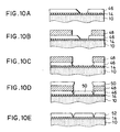
- a resist layer 48 which is patterned so as to be opened at a part including the chipped part 46 is formed (FIG. 10B).
- the part including the chipped part 46 is etched off with the resist layer 48 as the mask (FIG. 10C).
- a SiO 2 layer 50 of a required thickness which is to be the phase shifter is evaporated on the entire surface (FIG. 10D).
- the SiO 2 layer 50 is formed both on the etching stopping layer 14 and on the resist layer 48.
- Three chrome lines 12 are formed of a light shielding layer on a mask substrate of quartz.
- An etching stopping layer (not shown) is formed on the entire surface of the mask substrate 10 including the chrome lines 12.
- a 270° phase shifter 18 for shifting a phase by 270° is formed on the left one of two light transmitting areas between each of the chrome lines 12 and its adjacent one, and on a light transmitting area which is right of the right one of the two light transmitting areas between each of the chrome lines 12 and its adjacent one.
- the 270° phase shifters 18 are formed of, e.g., an about 570 nm-thickness SiO 2 layer.
- a 90° phase shifter 16 for shifting a phase by 90° is formed on the right one of the two light transmitting areas sandwiched by each of the chrome lines 12 and its adjacent one.
- the 90° phase shifter is formed of, e,g,. an about 190 nm-thickness SIO 2 layer.
- the 90° phase shifter 16 is formed uninterrupted up to the peripheral areas of the chrome lines 12, but an allowance is provided for a light transmitting area on the right side of the right 270° phase shifter.
- the 90° phase shifter 16 and each 270° phase shifter 18 are separated from each other by a light transmitting area without any phase shifter formed thereon or the light shielding areas of the chrome lines 12 formed thereon. Accordingly there is no part where a phase sharply shifts by an angle larger than 90°.
- the 90° phase shifter 16 and the 270° phase shifters 18 are not overlapped on each other. Accordingly as described above, corrections of possible defects of the 90° phase shifter 16 and the 270° phase shifters can be separately made.
- the etching stopping layer is formed on the mask substrate and the chrome layers, but instead may be formed on the mask substrate and below the chrome layers.
- the formation of the 90° phase shifters are followed by the formation of the 270° phase shifters, but reversely the formation of the 270° phase shifters is followed by the formation of the 90° phase shifters.
- the phase shifters are formed of SiO 2 , but may be formed of other materials. Especially in a case that there is the selectivity of an etching process between a material of the phase shifters and a material of the mask substrate, the phase shifter may be formed only by lift-off technique.
- the etching stopping layer may not be formed.
- the first area where the 90° phase shifter is formed and the second area where the 270° phase shifter are formed sandwich therebetween the third area where no light shielding area and no phase shifter is formed. Accordingly there is no part where an intensity is lowered even when a phase sharply shifts even by 180° in the light transmitting area. Furthermore, the 90° shifter and the 270° phase shifters are not overlapped. Accordingly if the 90° shifters and the 270° phase shifters should have defects, the defects could be separately corrected with ease. Thus, the present invention much contributes to optical lithography for ultra-micronized patterns of semiconductor integrated circuits and so on.
Landscapes
- Physics & Mathematics (AREA)
- General Physics & Mathematics (AREA)
- Preparing Plates And Mask In Photomechanical Process (AREA)
- Exposure And Positioning Against Photoresist Photosensitive Materials (AREA)
- Exposure Of Semiconductors, Excluding Electron Or Ion Beam Exposure (AREA)
Claims (7)
- Fotomaske mit Lichtabschirmbereichen mit einer lichtabschirmenden Schicht (12), die auf einem Maskensubstrat (10) ausgebildet ist, und einem Licht durchlassenden Bereich, der auf dem Maskensubstrat (10) durch die Lichtabschirmbereiche definiert ist, wobei der Licht durchlassende Bereich in einen ersten Bereich mit einem darauf ausgebildeten 90°-Phasenschieber (16) zur Verschiebung der Phase von durchgelassenem Licht um 90° + m x 360° (m = 0,1,2,...), einen zweiten Bereich mit einem darauf ausgebildeten 270°-Phasenschieber (18) zur Verschiebung der Phase von durchgelassenem Licht um 270° + n x 360° (n = 0,1,2,...), und einen dritten Bereich zum Verschieben der Phase von durchgelassenem Licht um 0° aufgeteilt ist, dadurch gekennzeichnet,
daß der erste und der zweite Bereich derart angeordnet sind, daß sie sich weder gegenseitig noch mit den Lichtabschirmbereichen oder dem zwischen ihnen positionierten dritten Bereich überlappen, so daß der erste und der zweite Bereich an keiner Stelle aneinander angrenzen. - Fotomaske nach Anspruch 1,
dadurch gekennzeichnet,daß die lichtabschirmende Schicht (12) mehrere lichtabschirmende Linien, die mehrere Licht durchlassende Zwischenräume zwischen ihnen definieren, aufweist;daß der 90°-Phasenschieber (16) in einem die lichtabschirmenden Linien und die Licht durchlassenden Zwischenräume umfangenden Bereich ausgebildet ist;daß der 90°-Phasenschieber (16) und der 270°-Phasenschieber (18) abwechselnd auf jedem der Licht durchlassenden Zwischenräume ausgebildet sind,daß die 90°-Phasenschieber (16) auf den Licht durchlassenden Zwischenräumen ohne Unterbrechung bis zu dem 90°-Phasenschieber (16) auf dem Umfangsbereich ausgebildet sind, unddaß Licht durchlassende Bereiche mit weder dem 90°-Phasenschieber noch dem 270°-Phasenschieber zwischen den 270°-Phasenschiebern (18) auf den Licht durchlassenden Zwischenräumen und dem 90°-Phasenschieber (16) auf dem umfangenden Bereich positioniert sind, so daß der 270°-Phasenschieber (18) an keiner Stelle an den 90°-Phasenschieber (16) angrenzt. - Fotomaske nach Anspruch 2,
dadurch gekennzeichnet,daß der 90°-Phasenschieber (16) auf dem Licht durchlassenden Zwischenraum ausgebildet ist, der an die lichtabschirmende Linie an der am weitesten außen liegenden Seite der lichtabschirmenden Linien angrenzt;daß der 270°-Phasenschieber (18) auf einem Bereich ausgebildet ist, der an die lichtabschirmende Linie an der am weitesten außen liegenden Seite der lichtabschirmenden Linien angrenzt; unddaß Licht durchlassende Bereiche mit weder dem 90°-Phasenschieber noch dem 270°-Phasenschieber zwischen den 270°-Phasenschiebern (18) auf dem Bereich und den 90°-Phasenschiebern (16) auf dem Umgebungsbereich positioniert sind. - Fotomaske nach einem der Ansprüche 1 bis 3,
dadurch gekennzeichnet,
daß eine Ätzsperrschicht (14) zum Blockieren des Ätzens des Maskensubstrats (10) auf dem Maskensubstrat (10) ausgebildet ist. - Fotomaske nach Anspruch 4,
dadurch gekennzeichnet,
daß die Ätzsperrschicht (14) in dem Licht durchlassenden Bereich und auf der lichtabschirmenden Schicht (12) in den Lichtabschirmbereichen ausgebildet ist. - Verfahren zur Herstellung einer Fotomaske nach einem der Ansprüche 1 bis 5 mit den Verfahrensschritten:Ausbilden einer lichtabschirmenden Schicht (12) auf Teilen der Oberfläche eines Maskensubstrates (10), die Lichtabschirmbereiche sein sollen, und Ausbilden einer Ätzsperrschicht (14) auf dem gesamten Bereich des Maskensubstrats (10);Ausbilden eines ersten Phasenschiebers (16) auf der gesamten Oberfläche zum Verschieben der Phase von durchgelassenem Licht um 90° + m x 360° (m = 0,1,2,...);Ausbilden einer ersten Resistschicht (22) auf einem ersten Bereich des Licht durchlassenden Bereiches, der nicht die lichtabschirmende Schicht (12) darauf ausgebildet hat;Wegätzen eines Teiles des ersten Phasenschiebers (16) mit der ersten Resistschicht (22) als Maske, um den ersten Phasenschieber (16) auf dem ersten Bereich zu belassen;Ausbilden einer zweiten Resistschicht (24) mit einer Öffnung, die einem zweiten Bereich des Licht durchlassenden Bereiches entspricht, wobei der erste und der zweite Bereich derart angeordnet sind, daß sie sich weder gegenseitig noch mit den Lichtabschirmbereichen oder einem dazwischen angeordneten dritten Bereich zum Verschieben der Phase von durchgelassenem Licht um 0° überlappen, so daß der erste und der zweite Bereich an keiner Stelle aneinander angrenzen;Ausbilden eines zweiten Phasenschiebers (18) auf der gesamten Oberfläche zum Verschieben der Phase von durchgelassenem Licht um 270° + n x 360° (n = 0,1,2,...); undEntfernen der zweiten Resistschicht (24), um den zweiten Phasenschieber abzuheben, um den zweiten Phasenschieber (18) auf dem zweiten Bereich zu belassen.
- Verfahren zur Herstellung einer Fotomaske nach einem der Ansprüche 1 bis 5 mit den Verfahrensschritten:Ausbilden einer lichtabschirmenden Schicht (12) auf Teilen der Oberfläche eines Maskensubstrates (10), die Lichtabschirmbereiche sein sollen, und Ausbilden einer Ätzsperrschicht (14) auf dem gesamten Bereich des Maskenbereichs (10);Ausbilden einer ersten Resistschicht (28) mit einer Öffnung, die einem ersten Bereich eines Licht durchlassenden Bereiches entspricht;Ausbilden eines ersten Phasenschiebers (16) auf der gesamten Oberfläche zum Verschieben der Phase von durchgelassenem Licht um 90° + m x 360° (m = 0,1,2...);Entfernen der ersten Resistschicht (28) zum Abheben des ersten Phasenschiebers und Belassen des ersten Phasenschiebers (16) auf dem ersten Bereich;Ausbilden einer zweiten Resistschicht (24) mit einer Öffnung, die einem zweiten Bereich des Licht durchlassenden Bereiches entspricht, wobei der erste und der zweite Bereich derart angeordnet sind, daß sie sich weder gegenseitig noch mit dem Lichtabschirmbereichen oder einem dazwischen positionierten dritten Bereich zum Verschieben der Phase von durchgelassenem Licht um 0° überlappen, so daß der erste und der zweite Bereich an keiner Stelle aneinander angrenzen;Ausbilden eines zweiten Phasenschiebers (18) auf der gesamten Oberfläche zum Verschieben der Phase von durchgelassenem Licht um 270° + n x 360°(n = 0,1,2,...); und Entfernen der zweiten Resistschicht (24), um den zweiten Phasenschieber abzuheben und den zweiten Phasenschieber (18) auf dem zweiten Bereich zu belassen.
Applications Claiming Priority (2)
| Application Number | Priority Date | Filing Date | Title |
|---|---|---|---|
| JP3190091A JPH0534897A (ja) | 1991-07-30 | 1991-07-30 | 光学マスク及びその製造方法 |
| JP190091/91 | 1991-07-30 |
Publications (2)
| Publication Number | Publication Date |
|---|---|
| EP0529338A1 EP0529338A1 (de) | 1993-03-03 |
| EP0529338B1 true EP0529338B1 (de) | 1998-11-11 |
Family
ID=16252221
Family Applications (1)
| Application Number | Title | Priority Date | Filing Date |
|---|---|---|---|
| EP92113030A Expired - Lifetime EP0529338B1 (de) | 1991-07-30 | 1992-07-30 | Photomaske und Verfahren zur Herstellung |
Country Status (5)
| Country | Link |
|---|---|
| US (1) | US5368963A (de) |
| EP (1) | EP0529338B1 (de) |
| JP (1) | JPH0534897A (de) |
| KR (1) | KR960004314B1 (de) |
| DE (1) | DE69227556T2 (de) |
Families Citing this family (14)
| Publication number | Priority date | Publication date | Assignee | Title |
|---|---|---|---|---|
| KR100298610B1 (ko) * | 1992-09-01 | 2001-11-30 | 기타지마 요시토시 | 위상쉬프트포토마스크,위상쉬프트포토마스크블랭크및이들의제조방법 |
| KR0138297B1 (ko) * | 1994-02-07 | 1998-06-01 | 김광호 | 포토 마스크 및 그 제조 방법 |
| KR0143340B1 (ko) * | 1994-09-09 | 1998-08-17 | 김주용 | 위상반전 마스크 |
| KR0147665B1 (ko) * | 1995-09-13 | 1998-10-01 | 김광호 | 변형조명방법, 이에 사용되는 반사경 및 그 제조방법 |
| US5948571A (en) * | 1997-03-12 | 1999-09-07 | International Business Machines Corporation | Asymmetrical resist sidewall |
| JPH10256394A (ja) | 1997-03-12 | 1998-09-25 | Internatl Business Mach Corp <Ibm> | 半導体構造体およびデバイス |
| US5985492A (en) * | 1998-01-22 | 1999-11-16 | International Business Machines Corporation | Multi-phase mask |
| US6090633A (en) * | 1999-09-22 | 2000-07-18 | International Business Machines Corporation | Multiple-plane pair thin-film structure and process of manufacture |
| JP2003173014A (ja) * | 2001-12-07 | 2003-06-20 | Mitsubishi Electric Corp | 位相シフトマスクの製造方法、位相シフトマスク、および、装置 |
| KR100853215B1 (ko) * | 2002-05-14 | 2008-08-20 | 삼성전자주식회사 | 액정 표시 장치 |
| KR100465067B1 (ko) * | 2002-06-19 | 2005-01-06 | 주식회사 하이닉스반도체 | 노광 마스크, 이의 제조 방법 및 이를 이용한 감광막 패턴형성 방법 |
| TWI316732B (en) * | 2005-09-09 | 2009-11-01 | Au Optronics Corp | Mask and manufacturing method thereof |
| CN1740909B (zh) * | 2005-09-26 | 2011-04-13 | 友达光电股份有限公司 | 光罩及其制造方法 |
| JP4879603B2 (ja) * | 2006-02-16 | 2012-02-22 | Hoya株式会社 | パターン形成方法及び位相シフトマスクの製造方法 |
Family Cites Families (5)
| Publication number | Priority date | Publication date | Assignee | Title |
|---|---|---|---|---|
| EP0653679B1 (de) * | 1989-04-28 | 2002-08-21 | Fujitsu Limited | Maske, Verfahren zur Herstellung der Maske und Verfahren zur Musterherstellung mit einer Maske |
| EP0437376B1 (de) * | 1990-01-12 | 1997-03-19 | Sony Corporation | Phasenverschiebungsmaske und Verfahren zur Herstellung |
| JPH0455854A (ja) * | 1990-06-25 | 1992-02-24 | Matsushita Electric Ind Co Ltd | フォトマスク装置およびこれを用いたパターン形成方法 |
| JPH04221954A (ja) * | 1990-12-25 | 1992-08-12 | Nec Corp | フォトマスク |
| US5229255A (en) * | 1991-03-22 | 1993-07-20 | At&T Bell Laboratories | Sub-micron device fabrication with a phase shift mask having multiple values of phase delay |
-
1991
- 1991-07-30 JP JP3190091A patent/JPH0534897A/ja active Pending
-
1992
- 1992-07-21 US US07/916,262 patent/US5368963A/en not_active Expired - Lifetime
- 1992-07-29 KR KR1019920013607A patent/KR960004314B1/ko not_active IP Right Cessation
- 1992-07-30 EP EP92113030A patent/EP0529338B1/de not_active Expired - Lifetime
- 1992-07-30 DE DE69227556T patent/DE69227556T2/de not_active Expired - Fee Related
Also Published As
| Publication number | Publication date |
|---|---|
| JPH0534897A (ja) | 1993-02-12 |
| US5368963A (en) | 1994-11-29 |
| KR930003267A (ko) | 1993-02-24 |
| EP0529338A1 (de) | 1993-03-03 |
| KR960004314B1 (ko) | 1996-03-30 |
| DE69227556T2 (de) | 1999-05-06 |
| DE69227556D1 (de) | 1998-12-17 |
Similar Documents
| Publication | Publication Date | Title |
|---|---|---|
| EP0529338B1 (de) | Photomaske und Verfahren zur Herstellung | |
| KR960010026B1 (ko) | 마스크가 사용되고 위상전이를 이용하는 패턴 노광 방법 | |
| KR100189668B1 (ko) | 위상 충돌을 피하기 위한 위상 쉬프트 리소그래피용 마스크 제조방법 | |
| KR100271699B1 (ko) | 포토마스크 및 포토마스크를 사용하는 반도체장치의 제조방법 | |
| US5487962A (en) | Method of chromeless phase shift mask fabrication suitable for auto-cad layout | |
| JP2000227652A (ja) | 半導体装置の製造方法 | |
| JPH04186244A (ja) | 露光方法 | |
| JP3977487B2 (ja) | 位相シフトマスクとその形成方法 | |
| US6180290B1 (en) | Multi-phase mask using multi-layer thin films | |
| JPH06301192A (ja) | ホトマスク | |
| US5942355A (en) | Method of fabricating a phase-shifting semiconductor photomask | |
| GB2286254A (en) | Phase shift mask and method for fabricating the same | |
| US5895735A (en) | Phase shift masks including first and second radiation blocking layer patterns, and methods of fabricating and using the same | |
| US6466373B1 (en) | Trimming mask with semitransparent phase-shifting regions | |
| US5464712A (en) | Method for fabricating a phase shifting mask | |
| US6479194B1 (en) | Transparent phase shift mask for fabrication of small feature sizes | |
| US6830853B1 (en) | Chrome mask dry etching process to reduce loading effect and defects | |
| KR100207473B1 (ko) | 위상반전마스크의 제작방법 | |
| US6312855B1 (en) | Three-phase phase shift mask | |
| KR100462887B1 (ko) | 필드 게이트 이미지의 폭을 보강하는 위상 에지 위상 변이마스크 및 제조방법 | |
| US6835506B2 (en) | Method for producing a photomask and corresponding photomask | |
| US6933085B1 (en) | Transparent phase shift mask for fabrication of small feature sizes | |
| JP3207470B2 (ja) | 位相差マスク | |
| JP3322007B2 (ja) | ハーフトーン方式位相シフトマスク及びレジスト露光方法 | |
| US20020177047A1 (en) | Photomask and method for manufacturing the same |
Legal Events
| Date | Code | Title | Description |
|---|---|---|---|
| PUAI | Public reference made under article 153(3) epc to a published international application that has entered the european phase |
Free format text: ORIGINAL CODE: 0009012 |
|
| AK | Designated contracting states |
Kind code of ref document: A1 Designated state(s): DE FR GB |
|
| 17P | Request for examination filed |
Effective date: 19930303 |
|
| 17Q | First examination report despatched |
Effective date: 19970204 |
|
| GRAG | Despatch of communication of intention to grant |
Free format text: ORIGINAL CODE: EPIDOS AGRA |
|
| GRAG | Despatch of communication of intention to grant |
Free format text: ORIGINAL CODE: EPIDOS AGRA |
|
| GRAH | Despatch of communication of intention to grant a patent |
Free format text: ORIGINAL CODE: EPIDOS IGRA |
|
| GRAH | Despatch of communication of intention to grant a patent |
Free format text: ORIGINAL CODE: EPIDOS IGRA |
|
| GRAA | (expected) grant |
Free format text: ORIGINAL CODE: 0009210 |
|
| AK | Designated contracting states |
Kind code of ref document: B1 Designated state(s): DE FR GB |
|
| PG25 | Lapsed in a contracting state [announced via postgrant information from national office to epo] |
Ref country code: FR Free format text: LAPSE BECAUSE OF FAILURE TO SUBMIT A TRANSLATION OF THE DESCRIPTION OR TO PAY THE FEE WITHIN THE PRESCRIBED TIME-LIMIT Effective date: 19981111 |
|
| REF | Corresponds to: |
Ref document number: 69227556 Country of ref document: DE Date of ref document: 19981217 |
|
| EN | Fr: translation not filed | ||
| PLBE | No opposition filed within time limit |
Free format text: ORIGINAL CODE: 0009261 |
|
| STAA | Information on the status of an ep patent application or granted ep patent |
Free format text: STATUS: NO OPPOSITION FILED WITHIN TIME LIMIT |
|
| 26N | No opposition filed | ||
| REG | Reference to a national code |
Ref country code: GB Ref legal event code: IF02 |
|
| PGFP | Annual fee paid to national office [announced via postgrant information from national office to epo] |
Ref country code: GB Payment date: 20060726 Year of fee payment: 15 |
|
| PGFP | Annual fee paid to national office [announced via postgrant information from national office to epo] |
Ref country code: DE Payment date: 20060727 Year of fee payment: 15 |
|
| GBPC | Gb: european patent ceased through non-payment of renewal fee |
Effective date: 20070730 |
|
| PG25 | Lapsed in a contracting state [announced via postgrant information from national office to epo] |
Ref country code: DE Free format text: LAPSE BECAUSE OF NON-PAYMENT OF DUE FEES Effective date: 20080201 |
|
| PG25 | Lapsed in a contracting state [announced via postgrant information from national office to epo] |
Ref country code: GB Free format text: LAPSE BECAUSE OF NON-PAYMENT OF DUE FEES Effective date: 20070730 |