EP0529338B1 - Photomask and method of fabricating the same - Google Patents

Photomask and method of fabricating the same Download PDF

Info

Publication number
EP0529338B1
EP0529338B1 EP92113030A EP92113030A EP0529338B1 EP 0529338 B1 EP0529338 B1 EP 0529338B1 EP 92113030 A EP92113030 A EP 92113030A EP 92113030 A EP92113030 A EP 92113030A EP 0529338 B1 EP0529338 B1 EP 0529338B1
Authority
EP
European Patent Office
Prior art keywords
phase shifter
area
phase
light
areas
Prior art date
Legal status (The legal status is an assumption and is not a legal conclusion. Google has not performed a legal analysis and makes no representation as to the accuracy of the status listed.)
Expired - Lifetime
Application number
EP92113030A
Other languages
German (de)
French (fr)
Other versions
EP0529338A1 (en
Inventor
Satoru c/o FUJITSU LIMITED Asai
Isamu c/o Fujitsu Limited Hanyu
Current Assignee (The listed assignees may be inaccurate. Google has not performed a legal analysis and makes no representation or warranty as to the accuracy of the list.)
Fujitsu Ltd
Original Assignee
Fujitsu Ltd
Priority date (The priority date is an assumption and is not a legal conclusion. Google has not performed a legal analysis and makes no representation as to the accuracy of the date listed.)
Filing date
Publication date
Application filed by Fujitsu Ltd filed Critical Fujitsu Ltd
Publication of EP0529338A1 publication Critical patent/EP0529338A1/en
Application granted granted Critical
Publication of EP0529338B1 publication Critical patent/EP0529338B1/en
Anticipated expiration legal-status Critical
Expired - Lifetime legal-status Critical Current

Links

Images

Classifications

    • GPHYSICS
    • G03PHOTOGRAPHY; CINEMATOGRAPHY; ANALOGOUS TECHNIQUES USING WAVES OTHER THAN OPTICAL WAVES; ELECTROGRAPHY; HOLOGRAPHY
    • G03FPHOTOMECHANICAL PRODUCTION OF TEXTURED OR PATTERNED SURFACES, e.g. FOR PRINTING, FOR PROCESSING OF SEMICONDUCTOR DEVICES; MATERIALS THEREFOR; ORIGINALS THEREFOR; APPARATUS SPECIALLY ADAPTED THEREFOR
    • G03F1/00Originals for photomechanical production of textured or patterned surfaces, e.g., masks, photo-masks, reticles; Mask blanks or pellicles therefor; Containers specially adapted therefor; Preparation thereof
    • G03F1/26Phase shift masks [PSM]; PSM blanks; Preparation thereof
    • G03F1/30Alternating PSM, e.g. Levenson-Shibuya PSM; Preparation thereof
    • GPHYSICS
    • G03PHOTOGRAPHY; CINEMATOGRAPHY; ANALOGOUS TECHNIQUES USING WAVES OTHER THAN OPTICAL WAVES; ELECTROGRAPHY; HOLOGRAPHY
    • G03FPHOTOMECHANICAL PRODUCTION OF TEXTURED OR PATTERNED SURFACES, e.g. FOR PRINTING, FOR PROCESSING OF SEMICONDUCTOR DEVICES; MATERIALS THEREFOR; ORIGINALS THEREFOR; APPARATUS SPECIALLY ADAPTED THEREFOR
    • G03F1/00Originals for photomechanical production of textured or patterned surfaces, e.g., masks, photo-masks, reticles; Mask blanks or pellicles therefor; Containers specially adapted therefor; Preparation thereof
    • G03F1/68Preparation processes not covered by groups G03F1/20 - G03F1/50
    • G03F1/80Etching
    • GPHYSICS
    • G03PHOTOGRAPHY; CINEMATOGRAPHY; ANALOGOUS TECHNIQUES USING WAVES OTHER THAN OPTICAL WAVES; ELECTROGRAPHY; HOLOGRAPHY
    • G03FPHOTOMECHANICAL PRODUCTION OF TEXTURED OR PATTERNED SURFACES, e.g. FOR PRINTING, FOR PROCESSING OF SEMICONDUCTOR DEVICES; MATERIALS THEREFOR; ORIGINALS THEREFOR; APPARATUS SPECIALLY ADAPTED THEREFOR
    • G03F1/00Originals for photomechanical production of textured or patterned surfaces, e.g., masks, photo-masks, reticles; Mask blanks or pellicles therefor; Containers specially adapted therefor; Preparation thereof
    • G03F1/26Phase shift masks [PSM]; PSM blanks; Preparation thereof
    • G03F1/28Phase shift masks [PSM]; PSM blanks; Preparation thereof with three or more diverse phases on the same PSM; Preparation thereof

Landscapes

  • Physics & Mathematics (AREA)
  • General Physics & Mathematics (AREA)
  • Preparing Plates And Mask In Photomechanical Process (AREA)
  • Exposure And Positioning Against Photoresist Photosensitive Materials (AREA)
  • Exposure Of Semiconductors, Excluding Electron Or Ion Beam Exposure (AREA)

Description

BACKGROUND OF THE INVENTION
The present invention relates to a photomask for use in optical lithography for the fabrication of semiconductor devices and so on, particularly to a photomask having phase shifters for shifting the phase of transmitted light, and to a method of fabricating the photomask.
Accompanying demands for larger-scales and higher integration of semiconductor integrated circuits in recent years, micronized patterning is required. To improve resolution for optical lithography using photomasks there have been proposed phase shift masks using phase shifters for shifting phases of transmitted light. A phase shift mask of e.g., a line and space pattern of alternated light shielding and light transmitting areas is intended to improve resolutions of patterns by setting at 180° a phase difference between light transmitting areas with light shielding areas therebetween.
But in the case a phase shift mask has a part in a light transmitting area, where a phase inversion of transmitted light takes place, i.e., an area (0° area) with no phase shifter formed thereon and an area (180° area) with a 180° phase shifter formed thereon are adjacent to each other, the intensity of the transmitted light is lowered at the part although the part is the light transmitting area. Consequently, by using such phase shift mask, resists adversely remain at parts where patterns are not to be formed. Attention has to be paid to arrangements of phase shifters so as not to form parts in light transmitting areas, where no phase inversions take place.
To remove such limitation to the arrangement of phase shifters, a 90° shifter, for example, is arranged at a part where a phase is inverted, whereby a sharp shift of a phase in a light transmitting area has been prevented.
Such conventional photomask is shown in FIG. 12. FIG. 12A is a plan view of the photomask, FIG. 12B is a sectional view along the line A-A' of FIG. 12A, and FIG. 12C is a sectional view along the line B-B' of FIG. 12A.
Chrome layers 102 are formed in lines on a mask substrate 100. To shift a phase by 180° in every two ones of light transmitting areas sandwiched by the chrome layers 102, phase shifters 104, 106 each for shifting a phase by 90° are superposed on each other, and the lower phase shifter 104 alone is formed on borders of the light transmitting areas with no phase shifter formed thereon. In the borders of the light transmitting area without the phase shifters a phase is bluntly shifted by 90°, so that no sharp phase shifts takes place.
Another conventional phase shift mask having phase shifters so arranged that the light transmitting area has no part where a phase is inverted in FIG. 13 (H. Ohtsuka et al., "Conjugate Twin-Shifter for the New Phase Shift Method to High Resolution Lithography", SPIE, Vol. 1463, pp. 112-123, Optical/Laser Microlithography IV (1991)). FIG. 13A is a plan view of the photomask, and FIG. 13B is a sectional view along the line A-A' of FIG. 13A.
In this conventional phase shifter, chrome layers 102 are formed on a mask substrate 100, and 90° phase sifters 108 for shifting a phase by 90° and 270° phase shifters 110 for shifting a phase by 270° are alternately formed on each of light transmitting areas sandwiched by the chrome layers 102,.
A phase is inverted in the boundary parts between the 90° phase shifter 108 and the 270° phase shifter 110. But in FIG. 13, because of the chrome layers 102 on the boundary parts, the light transmitting area has no parts where a phase inversion takes place.
But in such conventional phase shift mask as shown FIG. 12, to shift a phase by 180° in the light transmitting areas, the shifters 104, 106 each for shifting a phase by 90° are superposed on each other. If a defect is found in a phase shifter of the photomask, it will be difficult to correct the shifter alone separately.
The conventional shift mask of FIG. 13 has the problem that a light intensity is so lowered in the boundary parts of the phase shifters 108, 110 that a focus margin upon an exposure is lowered.
SUMMARY OF THE INVENTION
An object of the present invention is to provide a photomask and a method of fabricating the photomask, which can shift a phase in light transmitting areas without lowering the intensity of transmitted light, can easily correct defects of its phase shifters, and can secure a sufficient focus margin upon an exposure.
The object of the present invention is achieved by a photomask comprising light shielding areas with a light shielding layer formed on a mask substrate, and a light transmitting area defined on the mask substrate by the light shielding areas, the light transmitting area being divided in a first area with a 90° phase shifter formed thereon for shifting the phase of transmitted light by 90° + m x 360° (m=0,1,2,...), a second area with a 270° phase shifter formed thereon for shifting the phase of transmitted light by 270° + n x 360° (n=0,1,2,...), and a third area for shifting the phase of transmitted light by 0°, characterized by the first and the second areas being arranged without being overlapped on each other and with the light shielding areas or the third area located therebetween, so that the first and second areas are at no part adjacent to each other.
The object of the present invention is achieved by a method of fabricating a photomask according to claim 6, the method comprising the steps of forming a light shielding layer on parts of the surface to be light shielding areas, and forming an etching stopping layer on the entire area of the mask substrate, forming a first phase shifter on the entire surface for shifting the phase of transmitted light by 90° + m x 360° (m=0,1,2,...), forming a first resist layer on a first area of the light transmitting area not having the light shielding layer formed thereon, etching off a part of the first phase shifter with the first resist layer as a mask to leave the first phase shifter on the first area, forming a second resist layer with an opening corresponding to a second area of the light transmitting area, forming a second phase shifter on the entire surface for shifting the phase of the transmitted light by 270° + n x 360°(n=0,1,2,...), and removing the second resist layer to lift off the second phase shifter to leave the second phase shifter in the second area.
Alternatively, the photomask may be fabricated using the method of claim 7.
In the present invention, the first area with a 90° shifter formed on, and the second area with a 270° shifter formed on are arranged with a light shielding area or the third area with no phase shifter formed thereon located between the first and second areas. Consequently the photomask has no parts in the light transmitting area, where a phase of the transmitted light is sharply shifted, and consequently an intensity of the light is lowered. Furthermore, the 90° shifter and the 270° shifter are not overlapped on each other. Consequently even if a defect should take place in the 90° shifter or in the 270° shifter , the shifter could be easily corrected.
BRIEF DESCRIPTION OF THE DRAWINGS
  • Fig. 1 is a view of the photomask according to a first embodiment of the present invention;
  • Fig. 2 (2A and 2B) represents views of the photomask according to the first embodiment of the present invention;
  • Fig. 3 is a graph showing a relationship between focal points and minimum light intensity of the photomasks in Figs. 1 and 2, and Fig. 13;
  • Fig. 4 (4A-4C) represents sectional views (1) illustrative of the steps of a first embodiment of the method of fabricating the photomask of the present invention;
  • Fig. 5 (5A-5C) represents sectional views (2) illustrative of the steps of the first embodiment of the method of fabricating the photomask of the present invention;
  • Fig. 6 (6A-6D) represents sectional views (1) illustrative of the steps of a second embodiment of the method of fabricating the photomask of the present invention;
  • Fig. 7 (7A-7C represents sectional views (2) illustrative of the steps of the second embodiment of the method of fabricating the photomask of the present invention;
  • Fig. 8 (8A-8E) represents sectional views of the steps of a method of correcting the photomask according to the embodiment of the present invention;
  • Fig. 9 (9A-9D) represents sectional views of the steps of a method of correcting the photomask according to the embodiment of the present invention;
  • Fig. 10 (10A-10E) represents sectional views of the steps of a method of correcting the photomask according to the embodiment of the present invention;
  • Fig. 11 is a view of the photomask according to another embodiment of the present invention;
  • Fig. 12 (12A-12C) represents views of the conventional photomask; and
  • Fig. 13 (13A and 13B) represents views of the conventional photomask.
  • DETAILED DESCRIPTION OF THE INVENTION
    The photomask according to one embodiment of the present invention will be explained with reference to Figs. 1 and 2. Fig. 1 is a plan view of the photomask, Fig. 2A is a sectional view along the line A-A' of Fig. 1, and Fig. 2B is a sectional view along the line B-B' of Fig. 1.
    Four chrome lines 12 of a light shielding layer are formed on a mask substrate 10 of quartz. An etching stopping layer 14 for blocking etching is formed on the entire mask substrate 10 including the chrome layers 12. The etching stopping layer 14 is formed of, e.g. Al2O3.
    Three light transmitting areas are defined between adjacent ones of the four chrome lines 12, and a 90° phase shifter 16 for shifting a phase by 90° is formed on the central transmitting area of the three transmitting areas. The 90° phase shifter 16 is e. g. an about 190 nm-thickness SiO2 layer. This 90° phase shifter 16 is formed uninterruptedly up to the peripheral areas of the chrome lines 12.
    A 270° phase shifter 18 for shifting a phase by 270° is formed on each of the right and the left light transmitting areas of the three light transmitting areas sandwiched by each of the four chrome lines 12 and its adjacent one. The 270° phase shifters 18 are formed of e. g. an about 570 nm-thickness SiO2 layer. The 270° phase shifters 18 are formed only on the light transmitting areas between the chrome lines 12.
    The 90° phase shifter 16 is separated from the shorter sides of each of the 270° phase shifters 18 by light transmitting areas without any phase shifter formed thereon. The 90° phase shifter 16 is also separated from the longer sides of each of the 270° phase shifters 18 by the light shielding areas of the chrome lines 12.
    In the photomask according to this embodiment, the 90° phase shifter 16 and the 270° phase shifter 18 are separated from each other by the light transmitting areas without any phase shifter formed them or by the light shielding areas of the chrome lines 12, and accordingly there is no part where a phase sharply shifts by an angle larger than 90°. Furthermore, the 90° phase shifter 16 and the 270° phase shifter 18 are not overlapped on each other, and consequently possible defects of the 90° phase shifter 16 and the 270° phase shifter can be corrected separately.
    According to the photomask according to this embodiment, a light intensity is not lowered in the outer boundary part of the phase shifters, and consequently a sufficient focus margin can be secured upon an exposure.
    A minimum light intensity obtained when a focal point is shifted was calculated on the photomask according to this embodiment of FIGs. 1 and 2, and the conventional photomask of FIG. 13. In the photomask according to this embodiment of FIGs. 1 and 2, a light intensity is most lowered in the areas near the boundaries of the phase shifters 18. In the conventional photomask of FIG. 13, a light intensity is most lowered in the areas, which are boundary parts of the phase shifters 108, 110.
    The calculated results are shown in FIG.3. Focal points are taken on the horizontal axis, and minimum light intensities obtained at the respective focal points are taken on the vertical axis. The lower limit of the practically allowable light intensities was set at 0.4. As shown in FIG. 3, in the conventional photomask, the minimum light intensity exceeds the limit value 0.4 between the focal points -0.5 µm and +0.5 µm. In the photomask according to this embodiment, the minimum light intensity exceeded the limit value 0.4 between the focal points - 0.5 µm and +1.0 µm. The focal margin of the conventional photomask was 1.0 µm, and the photomask according to this embodiment was 1.5 µm, which is 1.5 time that of the conventional photomask.
    Next, a first embodiment of the method of fabricating the photomask of the present invention will be explained with reference to FIGs. 4 and 5.
    First, a chrome layer 12 is evaporated on the entire surface of a mask substrate 10 of quartz and is patterned in lines. Subsequently on the entire surface an etching stopping layer 14 of Al2O3 is evaporated. Then an about 190 nm-thickness SiO2 layer 20 is evaporated on the entire surface (FIG. 4A).
    Next, a resist layer 22 which is so patterned that a region for the 90° phase shifter 16 to be formed thereon is masked is formed (FIG. 4B).
    Then the SiO2 layer 20 is etched by, e.g., RIE (Reactive Ion Etching) with the resist layer 22 as the mask, and the 90° phase shifter 16 is formed (FIG. 4C). This etching of the SiO2 layer 20 is stopped at the etching stopping layer 14 and the surface of the mask substrate 10 is never etched.
    Subsequently a resist layer 24 which is so patterned that a region for the 270° phase shifter 18 to be formed thereon is opened is formed (FIG. 5A).
    Then an about 570 nm-thickness SiO2 layer 26 is evaporated on the entire surface (FIG 5B). The SiO2 layer 26 is formed both on the etching stopping layer 14 and on the resist layer 24.
    Next, the resist layer 24 is removed to lift off the resist layer 24 on the SiO2 layer 26, and the 270° phase shifter 18 is formed (FIG. 5C).
    In the method of fabricating the photomask illustrated in FIGs. 4 and 5, the 90° phase shifter 16 is formed by etching technique, and the 270° phase shifter 18 is formed by lift-off technique.
    Next, a second embodiment of the method of fabricating the photomask according of the present invention will be explained below with reference to FIGs. 6 and 7.
    First, a chrome layer 12 is evaporated on the entire surface of a mask substrate 10 of quartz, and is patterned in lines. Then an Al2O3 etching stopping layer 14 is evaporated on the entire surface (FIG. 6A).
    Then a resist layer 28 which is so patterned that a region for the 90° phase shifter 16 to be formed on is opened is formed (FIG. 6B).
    Next, an about 190 nm-thickness SiO2 layer 30 is evaporated on the entire surface (FIG. 6C). The SiO2 layer 28 is formed both on the etching stopping layer 14 and on the resist layer 28.
    Subsequently the resist layer 28 is removed to lift off the SiO2 layer 30 on the resist layer 28, and the 90° phase shifter 16 is formed (FIG. 6D).
    Then, similarly with the first embodiment, a resist layer 24 which is so patterned that a region for the 270° phase shifter to be formed is opened is formed (FIG. 7A), and an about 570 nm-thickness SiO2 layer 26 is evaporated on the entire surface (FIG. 7B). The SiO2 layer 26 on the resist layer 24 is lifted off, and the 270° phase shifter 18 is formed (FIG. 7C).
    In the method of fabricating the photomask illustrated in FIGs. 6 and 7, both the 90° phase shifter 16 and the 270° phase shifter 18 are formed by lift-off technique.
    Methods of correcting the photomask according to the above-described embodiment will be explained below with reference to FIGs. 8, 9 and 10.
    With reference to FIG. 8, a method of correcting the photomask will be explained by means of a case that the 90° phase shifter 16 or the 270° phase shifter has a chipped pattern 32 (FIG. 8A).
    A resist layer 34 which is patterned so as to be opened at a part corresponding to the chipped pattern 32 is formed (FIG. 8B).
    Then the chipped pattern is etched off with the resist layer 34 as the mask (FIG. 8C).
    Subsequently a SiO2 layer 36 of a required thickness which is to be the phase shifter is evaporated on the entire surface (FIG. 8D). The SiO2 layer 36 is formed both on the etching stopping layer 14 and on the resist layer 34.
    Then the resist layer 34 is removed to lift off the SiO2 layer 36 on the resist layer 34, and a perfect phase shifter 38 without any defect is formed (FIG. 8E).
    With reference to FIG. 9 a method of correcting the photomask will be explained by means of a case that a residual pattern 40 is present at a part where neither a 90° phase shifter 16 nor the 270° phase shifter 18 should be formed (FIG. 9A).
    First a resist layer 42 which is patterned so as to be opened at a part corresponding to the residual pattern 40 (FIG. 9B). A normal pattern 44 is covered protectively with the resist layer 42.
    Then only the residual pattern 40 is etched off with the resist layer 44 as the mask (FIG. 9C).
    Subsequently the resist layer 44 is removed to leave only the normal pattern 44 (FIG. 9D).
    In the photomask according to the embodiments of the present invention, the 90° phase shifter 16 and the 270° phase shifters 18 are not overlapped on each other. Consequently corrections of possible defects of the 90° phase shifter 16 and of the 270° phase shifter 18 can be made separately.
    With reference to FIG. 10, a method of correcting the photomask will be explained by means of a case that the 90° phase shifter 16 or the 270° phase shifter has a chipped part 46 (FIG. 10A).
    A resist layer 48 which is patterned so as to be opened at a part including the chipped part 46 is formed (FIG. 10B).
    Then the part including the chipped part 46 is etched off with the resist layer 48 as the mask (FIG. 10C).
    Subsequently a SiO2 layer 50 of a required thickness which is to be the phase shifter is evaporated on the entire surface (FIG. 10D). The SiO2 layer 50 is formed both on the etching stopping layer 14 and on the resist layer 48.
    Then the resist layer 48 is removed to lift off the SiO2 layer 50 on the resist layer 48, and a perfect phase shifter 52 without any defect is formed (FIG. 10E).
    Next, the photomask according to further another embodiment of the present invention will be explained below with reference to the plan view of FIG. 11.
    Three chrome lines 12 are formed of a light shielding layer on a mask substrate of quartz. An etching stopping layer (not shown) is formed on the entire surface of the mask substrate 10 including the chrome lines 12.
    A 270° phase shifter 18 for shifting a phase by 270° is formed on the left one of two light transmitting areas between each of the chrome lines 12 and its adjacent one, and on a light transmitting area which is right of the right one of the two light transmitting areas between each of the chrome lines 12 and its adjacent one. The 270° phase shifters 18 are formed of, e.g., an about 570 nm-thickness SiO2 layer.
    A 90° phase shifter 16 for shifting a phase by 90° is formed on the right one of the two light transmitting areas sandwiched by each of the chrome lines 12 and its adjacent one. The 90° phase shifter is formed of, e,g,. an about 190 nm-thickness SIO2 layer. The 90° phase shifter 16 is formed uninterrupted up to the peripheral areas of the chrome lines 12, but an allowance is provided for a light transmitting area on the right side of the right 270° phase shifter.
    In the photomask according to this embodiment, the 90° phase shifter 16 and each 270° phase shifter 18 are separated from each other by a light transmitting area without any phase shifter formed thereon or the light shielding areas of the chrome lines 12 formed thereon. Accordingly there is no part where a phase sharply shifts by an angle larger than 90°. The 90° phase shifter 16 and the 270° phase shifters 18 are not overlapped on each other. Accordingly as described above, corrections of possible defects of the 90° phase shifter 16 and the 270° phase shifters can be separately made.
    The present invention is not limited to the above-described embodiments and can cover other different variations and modifications.
    In the above-described embodiments, for example, the etching stopping layer is formed on the mask substrate and the chrome layers, but instead may be formed on the mask substrate and below the chrome layers.
    In the above-described embodiments, the formation of the 90° phase shifters are followed by the formation of the 270° phase shifters, but reversely the formation of the 270° phase shifters is followed by the formation of the 90° phase shifters.
    In the above-described embodiments, the phase shifters are formed of SiO2, but may be formed of other materials. Especially in a case that there is the selectivity of an etching process between a material of the phase shifters and a material of the mask substrate, the phase shifter may be formed only by lift-off technique.
    In a case that defect corrections of a phase shifter pattern are not necessary, the etching stopping layer may not be formed.
    As described above, according to the present invention, the first area where the 90° phase shifter is formed and the second area where the 270° phase shifter are formed sandwich therebetween the third area where no light shielding area and no phase shifter is formed. Accordingly there is no part where an intensity is lowered even when a phase sharply shifts even by 180° in the light transmitting area. Furthermore, the 90° shifter and the 270° phase shifters are not overlapped. Accordingly if the 90° shifters and the 270° phase shifters should have defects, the defects could be separately corrected with ease. Thus, the present invention much contributes to optical lithography for ultra-micronized patterns of semiconductor integrated circuits and so on.

    Claims (7)

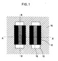
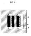
    1. A photomask comprising light shielding areas with a light shielding layer (12) formed on a mask substrate (10) and a light transmitting area defined on the mask substrate (10) by the light shielding areas,
      the light transmitting area being devided in a first area with a 90° phase shifter (16) formed thereon for shifting the phase of transmitted light by 90° + m x 360° (m=0,1,2,...), a second area with a 270° phase shifter (18) formed thereon for shifting the phase of transmitted light by 270° + n x 360° (n=0,1,2,...), and a third area for shifting the phase of transmitted light by 0°, characterized by
      the first and the second areas being arranged without being overlapped on each other and with the light shielding areas or the third area located therebetween, so that the first and second areas are at no part adjacent to each other.
    2. A photomask according to claim 1, wherein
      the light shielding layer (12) has a plurality of light shielding lines, which define a plurality of light transmitting spaces therebetween;
      the 90° phase shifter (16) is formed on a peripheral area of the light shielding lines and the light transmitting spaces;
      the 90° phase shifter (16) and the 270° phase shifter (18) are alternately formed on each of the light transmitting spaces;
      the 90° phase shifters (16) on the light transmitting spaces are formed uninterruptedly up to the 90° phase shifter (16) on the peripheral area; and
      light transmitting areas with neither the 90° phase shifter nor the 270° phase shifter are located between the 270° phase shifters (18) on the light transmitting spaces and the 90° phase shifter (16) on the peripheral area, so that the 270° phase shifter (18) is at no part adjacent to the 90° phase shifter (16).
    3. A photomask according to claim 2, wherein
      the 90° phase shifter (16) is formed on the light transmitting space adjacent to the light shielding line at the most outer side of the light shielding lines;
      the 270° phase shifter (18) is formed on an area adjacent to the light shielding line at the most outer side of the light shielding lines; and
      light transmitting areas with neither the 90° phase shifter nor the 270° phase shifter are located between the 270° phase shifters (18) on the area and the 90° phase shifter (16) on the peripheral area.
    4. A photomask according to any one of claims 1 to 3, wherein
      an etching stopping layer (14) for blocking etching of the mask substrate (10) is formed on the mask substrate (10).
    5. A photomask according to claim 4, wherein the
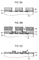
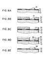
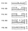
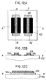
      etching stopping layer (14) is formed in the light transmitting area and on the light shielding layer (12) in the light shielding areas.
    6. A method of fabricating a photomask according to any one of claims 1 to 5, comprising the steps of:
      forming a light shielding layer (12) on parts of the surface of a mask substrate (10) to be light shielding areas, and forming an etching stopping layer (14) on the entire area of the mask substrate (10);
      forming a first phase shifter (16) on the entire surface for shifting the phase of transmitted light by 90° + m x 360° (m=0,1,2,...);
      forming a first resist layer (22) on a first area of the light transmitting area not having the light shielding layer (12) formed thereon;
      etching off a part of the first phase shifter (16) with the first resist layer (22) as a mask to leave the first phase shifter (16) on the first area;
      forming a second resist layer (24) with an opening corresponding to a second area of the light transmitting area, the first and the second areas being arranged without being overlapped on each other and with the light shielding areas or a third area for shifting the phase of transmitted light by 0° located therebetween, so that the first and second areas are at no part adjacent to each other;
      forming a second phase shifter (18) on the entire surface for shifting the phase of transmitted light by 270° + n x 360° (n=0,1,2,...); and
      removing the second resist layer (24) to lift off the second phase shifter to leave the second phase shifter (18) on the second area.
    7. A method of fabricating a photomask according to any one of claims 1 to 5, comprising the steps of:
      forming a light shielding layer (12) on parts of the surface of a mask substrate (10) to be light shielding areas, and forming an etching stopping layer (14) on the entire area of the mask substrate (10);
      forming a first resist layer (28) with an opening corresponding to a first area of a light transmitting area;
      forming a first phase shifter (16) on the entire surface for shifting the phase of transmitted light by 90° + m x 360° (m=0,1,2,...);
      removing the first resist layer (28) to lift off the first phase shifter and leaving the first phase shifter (16) on the first area;
      forming a second resist layer (24) with an opening corresponding to a second area of the light transmitting area, the first and the second areas being arranged without being overlapped on each other and with the light shielding areas or a third area for shifting the phase of transmitted light by 0° located therebetween, so that the first and second areas are at no part adjacent to each other;
      forming a second phase shifter (18) on the entire surface for shifting the phase of transmitted light by 270° + n x 360° (n=0,1,2,...); and
      removing the second resist layer (24) to lift off the second phase shifter and leaving the second phase shifter (18) on the second area.
    EP92113030A 1991-07-30 1992-07-30 Photomask and method of fabricating the same Expired - Lifetime EP0529338B1 (en)

    Applications Claiming Priority (2)

    Application Number Priority Date Filing Date Title
    JP3190091A JPH0534897A (en) 1991-07-30 1991-07-30 Optical mask and production thereof
    JP190091/91 1991-07-30

    Publications (2)

    Publication Number Publication Date
    EP0529338A1 EP0529338A1 (en) 1993-03-03
    EP0529338B1 true EP0529338B1 (en) 1998-11-11

    Family

    ID=16252221

    Family Applications (1)

    Application Number Title Priority Date Filing Date
    EP92113030A Expired - Lifetime EP0529338B1 (en) 1991-07-30 1992-07-30 Photomask and method of fabricating the same

    Country Status (5)

    Country Link
    US (1) US5368963A (en)
    EP (1) EP0529338B1 (en)
    JP (1) JPH0534897A (en)
    KR (1) KR960004314B1 (en)
    DE (1) DE69227556T2 (en)

    Families Citing this family (14)

    * Cited by examiner, † Cited by third party
    Publication number Priority date Publication date Assignee Title
    DE69328220T2 (en) * 1992-09-01 2000-08-24 Dainippon Printing Co Ltd Process for the production of a phase shift mask or a phase shift mask blank
    KR0138297B1 (en) * 1994-02-07 1998-06-01 김광호 Photo-mask and fabrication method thereof
    KR0143340B1 (en) * 1994-09-09 1998-08-17 김주용 Phase shift mask
    KR0147665B1 (en) * 1995-09-13 1998-10-01 김광호 Changing illumination method reflection mirror and making method used thereof
    US5948571A (en) * 1997-03-12 1999-09-07 International Business Machines Corporation Asymmetrical resist sidewall
    JPH10256394A (en) 1997-03-12 1998-09-25 Internatl Business Mach Corp <Ibm> Semiconductor structure and device
    US5985492A (en) * 1998-01-22 1999-11-16 International Business Machines Corporation Multi-phase mask
    US6090633A (en) * 1999-09-22 2000-07-18 International Business Machines Corporation Multiple-plane pair thin-film structure and process of manufacture
    JP2003173014A (en) * 2001-12-07 2003-06-20 Mitsubishi Electric Corp Method of manufacturing phase shift mask, phase shift mask and device
    KR100853215B1 (en) * 2002-05-14 2008-08-20 삼성전자주식회사 Liquid crystal display
    KR100465067B1 (en) * 2002-06-19 2005-01-06 주식회사 하이닉스반도체 Photo mask, method of manufacturing the same and method of forming a photosensitive film pattern of using the same
    TWI316732B (en) * 2005-09-09 2009-11-01 Au Optronics Corp Mask and manufacturing method thereof
    CN1740909B (en) * 2005-09-26 2011-04-13 友达光电股份有限公司 Optical mask and producing method thereof
    JP4879603B2 (en) * 2006-02-16 2012-02-22 Hoya株式会社 Pattern forming method and phase shift mask manufacturing method

    Family Cites Families (5)

    * Cited by examiner, † Cited by third party
    Publication number Priority date Publication date Assignee Title
    JP2862183B2 (en) * 1989-04-28 1999-02-24 富士通株式会社 Manufacturing method of mask
    EP0730200A3 (en) * 1990-01-12 1997-01-22 Sony Corp Phase shifting masks and methods of manufacture
    JPH0455854A (en) * 1990-06-25 1992-02-24 Matsushita Electric Ind Co Ltd Photomask device and pattern forming method using this device
    JPH04221954A (en) * 1990-12-25 1992-08-12 Nec Corp Photomask
    US5229255A (en) * 1991-03-22 1993-07-20 At&T Bell Laboratories Sub-micron device fabrication with a phase shift mask having multiple values of phase delay

    Also Published As

    Publication number Publication date
    KR960004314B1 (en) 1996-03-30
    US5368963A (en) 1994-11-29
    DE69227556D1 (en) 1998-12-17
    KR930003267A (en) 1993-02-24
    EP0529338A1 (en) 1993-03-03
    DE69227556T2 (en) 1999-05-06
    JPH0534897A (en) 1993-02-12

    Similar Documents

    Publication Publication Date Title
    EP0529338B1 (en) Photomask and method of fabricating the same
    KR960010026B1 (en) Pattern exposing method using phase shift and mask used therefor
    KR100189668B1 (en) Phase shifting mask
    KR100271699B1 (en) Photmask and method for manufacturing semiconductor device using photomask
    US5487962A (en) Method of chromeless phase shift mask fabrication suitable for auto-cad layout
    JPH07281413A (en) Attenuation type phase shift mask and its production
    JP2000227652A (en) Production of semiconductor device
    JPH04186244A (en) Photomask and exposure
    JP3977487B2 (en) Phase shift mask and method for forming the same
    US6180290B1 (en) Multi-phase mask using multi-layer thin films
    JPH06301192A (en) Photo-mask
    US5942355A (en) Method of fabricating a phase-shifting semiconductor photomask
    GB2286254A (en) Phase shift mask and method for fabricating the same
    US5895735A (en) Phase shift masks including first and second radiation blocking layer patterns, and methods of fabricating and using the same
    US6466373B1 (en) Trimming mask with semitransparent phase-shifting regions
    US5464712A (en) Method for fabricating a phase shifting mask
    US6479194B1 (en) Transparent phase shift mask for fabrication of small feature sizes
    KR100207473B1 (en) Phase shift mask manufacturing method
    US6312855B1 (en) Three-phase phase shift mask
    US6835506B2 (en) Method for producing a photomask and corresponding photomask
    US7097949B2 (en) Phase edge phase shift mask enforcing a width of a field gate image and fabrication method thereof
    US6933085B1 (en) Transparent phase shift mask for fabrication of small feature sizes
    JP3207470B2 (en) Phase difference mask
    JP3322007B2 (en) Halftone phase shift mask and resist exposure method
    US20020177047A1 (en) Photomask and method for manufacturing the same

    Legal Events

    Date Code Title Description
    PUAI Public reference made under article 153(3) epc to a published international application that has entered the european phase

    Free format text: ORIGINAL CODE: 0009012

    AK Designated contracting states

    Kind code of ref document: A1

    Designated state(s): DE FR GB

    17P Request for examination filed

    Effective date: 19930303

    17Q First examination report despatched

    Effective date: 19970204

    GRAG Despatch of communication of intention to grant

    Free format text: ORIGINAL CODE: EPIDOS AGRA

    GRAG Despatch of communication of intention to grant

    Free format text: ORIGINAL CODE: EPIDOS AGRA

    GRAH Despatch of communication of intention to grant a patent

    Free format text: ORIGINAL CODE: EPIDOS IGRA

    GRAH Despatch of communication of intention to grant a patent

    Free format text: ORIGINAL CODE: EPIDOS IGRA

    GRAA (expected) grant

    Free format text: ORIGINAL CODE: 0009210

    AK Designated contracting states

    Kind code of ref document: B1

    Designated state(s): DE FR GB

    PG25 Lapsed in a contracting state [announced via postgrant information from national office to epo]

    Ref country code: FR

    Free format text: LAPSE BECAUSE OF FAILURE TO SUBMIT A TRANSLATION OF THE DESCRIPTION OR TO PAY THE FEE WITHIN THE PRESCRIBED TIME-LIMIT

    Effective date: 19981111

    REF Corresponds to:

    Ref document number: 69227556

    Country of ref document: DE

    Date of ref document: 19981217

    EN Fr: translation not filed
    PLBE No opposition filed within time limit

    Free format text: ORIGINAL CODE: 0009261

    STAA Information on the status of an ep patent application or granted ep patent

    Free format text: STATUS: NO OPPOSITION FILED WITHIN TIME LIMIT

    26N No opposition filed
    REG Reference to a national code

    Ref country code: GB

    Ref legal event code: IF02

    PGFP Annual fee paid to national office [announced via postgrant information from national office to epo]

    Ref country code: GB

    Payment date: 20060726

    Year of fee payment: 15

    PGFP Annual fee paid to national office [announced via postgrant information from national office to epo]

    Ref country code: DE

    Payment date: 20060727

    Year of fee payment: 15

    GBPC Gb: european patent ceased through non-payment of renewal fee

    Effective date: 20070730

    PG25 Lapsed in a contracting state [announced via postgrant information from national office to epo]

    Ref country code: DE

    Free format text: LAPSE BECAUSE OF NON-PAYMENT OF DUE FEES

    Effective date: 20080201

    PG25 Lapsed in a contracting state [announced via postgrant information from national office to epo]

    Ref country code: GB

    Free format text: LAPSE BECAUSE OF NON-PAYMENT OF DUE FEES

    Effective date: 20070730