EP0525650B1 - Verfahren zur Herstellung einer Halbleitervorrichtung mit einer isolierenden Schicht für einen Kondensator - Google Patents
Verfahren zur Herstellung einer Halbleitervorrichtung mit einer isolierenden Schicht für einen Kondensator Download PDFInfo
- Publication number
- EP0525650B1 EP0525650B1 EP92112613A EP92112613A EP0525650B1 EP 0525650 B1 EP0525650 B1 EP 0525650B1 EP 92112613 A EP92112613 A EP 92112613A EP 92112613 A EP92112613 A EP 92112613A EP 0525650 B1 EP0525650 B1 EP 0525650B1
- Authority
- EP
- European Patent Office
- Prior art keywords
- silicon nitride
- nitride film
- film
- insulating film
- semiconductor device
- Prior art date
- Legal status (The legal status is an assumption and is not a legal conclusion. Google has not performed a legal analysis and makes no representation as to the accuracy of the status listed.)
- Expired - Lifetime
Links
Images


Classifications
-
- H—ELECTRICITY
- H10—SEMICONDUCTOR DEVICES; ELECTRIC SOLID-STATE DEVICES NOT OTHERWISE PROVIDED FOR
- H10P—GENERIC PROCESSES OR APPARATUS FOR THE MANUFACTURE OR TREATMENT OF DEVICES COVERED BY CLASS H10
- H10P14/00—Formation of materials, e.g. in the shape of layers or pillars
- H10P14/60—Formation of materials, e.g. in the shape of layers or pillars of insulating materials
- H10P14/69—Inorganic materials
- H10P14/694—Inorganic materials composed of nitrides
- H10P14/6943—Inorganic materials composed of nitrides containing silicon
- H10P14/69433—Inorganic materials composed of nitrides containing silicon the material being a silicon nitride not containing oxygen, e.g. SixNy or SixByNz
-
- H—ELECTRICITY
- H10—SEMICONDUCTOR DEVICES; ELECTRIC SOLID-STATE DEVICES NOT OTHERWISE PROVIDED FOR
- H10D—INORGANIC ELECTRIC SEMICONDUCTOR DEVICES
- H10D1/00—Resistors, capacitors or inductors
- H10D1/60—Capacitors
- H10D1/68—Capacitors having no potential barriers
-
- H—ELECTRICITY
- H10—SEMICONDUCTOR DEVICES; ELECTRIC SOLID-STATE DEVICES NOT OTHERWISE PROVIDED FOR
- H10D—INORGANIC ELECTRIC SEMICONDUCTOR DEVICES
- H10D30/00—Field-effect transistors [FET]
- H10D30/60—Insulated-gate field-effect transistors [IGFET]
- H10D30/67—Thin-film transistors [TFT]
- H10D30/6729—Thin-film transistors [TFT] characterised by the electrodes
- H10D30/6737—Thin-film transistors [TFT] characterised by the electrodes characterised by the electrode materials
- H10D30/6739—Conductor-insulator-semiconductor electrodes
-
- H—ELECTRICITY
- H10—SEMICONDUCTOR DEVICES; ELECTRIC SOLID-STATE DEVICES NOT OTHERWISE PROVIDED FOR
- H10P—GENERIC PROCESSES OR APPARATUS FOR THE MANUFACTURE OR TREATMENT OF DEVICES COVERED BY CLASS H10
- H10P14/00—Formation of materials, e.g. in the shape of layers or pillars
- H10P14/60—Formation of materials, e.g. in the shape of layers or pillars of insulating materials
- H10P14/63—Formation of materials, e.g. in the shape of layers or pillars of insulating materials characterised by the formation processes
- H10P14/6302—Non-deposition formation processes
- H10P14/6316—Formation by nitridation, e.g. nitridation of the substrate
-
- H—ELECTRICITY
- H10—SEMICONDUCTOR DEVICES; ELECTRIC SOLID-STATE DEVICES NOT OTHERWISE PROVIDED FOR
- H10P—GENERIC PROCESSES OR APPARATUS FOR THE MANUFACTURE OR TREATMENT OF DEVICES COVERED BY CLASS H10
- H10P14/00—Formation of materials, e.g. in the shape of layers or pillars
- H10P14/60—Formation of materials, e.g. in the shape of layers or pillars of insulating materials
- H10P14/63—Formation of materials, e.g. in the shape of layers or pillars of insulating materials characterised by the formation processes
- H10P14/6302—Non-deposition formation processes
- H10P14/6322—Formation by thermal treatments
-
- H—ELECTRICITY
- H10—SEMICONDUCTOR DEVICES; ELECTRIC SOLID-STATE DEVICES NOT OTHERWISE PROVIDED FOR
- H10P—GENERIC PROCESSES OR APPARATUS FOR THE MANUFACTURE OR TREATMENT OF DEVICES COVERED BY CLASS H10
- H10P14/00—Formation of materials, e.g. in the shape of layers or pillars
- H10P14/60—Formation of materials, e.g. in the shape of layers or pillars of insulating materials
- H10P14/63—Formation of materials, e.g. in the shape of layers or pillars of insulating materials characterised by the formation processes
- H10P14/6326—Deposition processes
- H10P14/6328—Deposition from the gas or vapour phase
- H10P14/6334—Deposition from the gas or vapour phase using decomposition or reaction of gaseous or vapour phase compounds, i.e. chemical vapour deposition
-
- H—ELECTRICITY
- H10—SEMICONDUCTOR DEVICES; ELECTRIC SOLID-STATE DEVICES NOT OTHERWISE PROVIDED FOR
- H10P—GENERIC PROCESSES OR APPARATUS FOR THE MANUFACTURE OR TREATMENT OF DEVICES COVERED BY CLASS H10
- H10P14/00—Formation of materials, e.g. in the shape of layers or pillars
- H10P14/60—Formation of materials, e.g. in the shape of layers or pillars of insulating materials
- H10P14/65—Formation of materials, e.g. in the shape of layers or pillars of insulating materials characterised by treatments performed before or after the formation of the materials
- H10P14/6516—Formation of materials, e.g. in the shape of layers or pillars of insulating materials characterised by treatments performed before or after the formation of the materials of treatments performed after formation of the materials
- H10P14/6518—Formation of materials, e.g. in the shape of layers or pillars of insulating materials characterised by treatments performed before or after the formation of the materials of treatments performed after formation of the materials by introduction of substances into an already-existing insulating layer
- H10P14/6519—Formation of materials, e.g. in the shape of layers or pillars of insulating materials characterised by treatments performed before or after the formation of the materials of treatments performed after formation of the materials by introduction of substances into an already-existing insulating layer the substance being oxygen
- H10P14/6522—Formation of materials, e.g. in the shape of layers or pillars of insulating materials characterised by treatments performed before or after the formation of the materials of treatments performed after formation of the materials by introduction of substances into an already-existing insulating layer the substance being oxygen introduced into a nitride material, e.g. changing SiN to SiON
-
- H—ELECTRICITY
- H10—SEMICONDUCTOR DEVICES; ELECTRIC SOLID-STATE DEVICES NOT OTHERWISE PROVIDED FOR
- H10P—GENERIC PROCESSES OR APPARATUS FOR THE MANUFACTURE OR TREATMENT OF DEVICES COVERED BY CLASS H10
- H10P14/00—Formation of materials, e.g. in the shape of layers or pillars
- H10P14/60—Formation of materials, e.g. in the shape of layers or pillars of insulating materials
- H10P14/66—Formation of materials, e.g. in the shape of layers or pillars of insulating materials characterised by the type of materials
- H10P14/662—Laminate layers, e.g. stacks of alternating high-k metal oxides
-
- H—ELECTRICITY
- H10—SEMICONDUCTOR DEVICES; ELECTRIC SOLID-STATE DEVICES NOT OTHERWISE PROVIDED FOR
- H10P—GENERIC PROCESSES OR APPARATUS FOR THE MANUFACTURE OR TREATMENT OF DEVICES COVERED BY CLASS H10
- H10P14/00—Formation of materials, e.g. in the shape of layers or pillars
- H10P14/60—Formation of materials, e.g. in the shape of layers or pillars of insulating materials
- H10P14/69—Inorganic materials
- H10P14/692—Inorganic materials composed of oxides, glassy oxides or oxide-based glasses
- H10P14/6921—Inorganic materials composed of oxides, glassy oxides or oxide-based glasses containing silicon
- H10P14/69215—Inorganic materials composed of oxides, glassy oxides or oxide-based glasses containing silicon the material being a silicon oxide, e.g. SiO2
Definitions
- the present invention relates to a semiconductor device and a method for fabricating it, and more particularly to a structure of a capacitor insulating film and a method for fabricating it.
- capacitor insulating films there are used a silicon oxide film (SiO 2 ), a silicon nitride film (Si 3 N 4 ) and a composite film of these films (e.g., a double layered film of SiO 2 /Si 3 N 4 , and a triple layered film of SiO 2 /Si 3 N 4 /SiO 2 ).
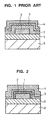
- Fig. 1 shows the structure of one example of these conventional films.
- a lower electrode 3 having a predetermined shape and made of impurity-doped polysilicon (also called polycrystalline silicon) is formed on the surface of the silicon oxide film 5 on a semiconductor substrate 6.
- a silicon nitride film 2 having a thickness of about 10 nm is formed by chemical vapor deposition techniques so as to cover the surface of the lower electrode 3. Thereafter, the surface of the silicon nitride film 2 is thermally oxidized to be converted into a silicon oxide film 7 having a thickness of about 2 - 3 nm. Subsequently, an upper electrode 4 made of polysilicon is formed so as to cover the silicon oxide film 7.
- the capacitor insulating film is composed of the silicon nitride film 2 formed by the chemical vapor deposition and the silicon oxide film 7 formed by the thermal oxidation. The capacitor insulating film has a thickness of about 7 - 8 nm in equivalent thickness of an oxide film. Reference is made to "Y. Ohji et al., Proceedings of 25th Annual IEEE Reliability Physics Symposium (1987) p. 55".
- the conventional capacitor insulating film has the following defects.
- the conventional silicon nitride film formed by the chemical vapor deposition contains many weak-spots so that a single silicon nitride film of 8 nm or less presents difficulties in its use as a stabilized capacitor insulating film with less leakage current. For this reason, a double layered SiO 2 /Si 3 N 4 film wherein the weak spots are covered by oxidation film on the surface of the silicon nitride film is now widely used in the current DRAMs, etc.
- this double layered film when it has a thickness of 5 nm or less in equivalent thickness of an oxide film, also suffers from an abrupt increase in the leakage current. Reference is made to "J. Yugami et al., Extended Abstracts on the 20th Conference on Solid State Devices and Materials (1988) p. 173".
- the chemical vapor deposition tends to introduce oxygen into the silicon nitride film. This introduction of oxygen is remarkable particularly in the initial process where the silicon nitride film grows on the oxide film. Also where a silicon nitride film is to be grown on polysilicon from a vapor phase, it will actually grow on the native oxide film formed on the polysilicon surface. Thus, it was difficult to form a stoichiometric silicon nitride film of 10 nm or less thickness on polysilicon by the chemical vapor deposition techniques. Reference is made to "J. A. Wurzbach and F. J. Grunthaner, J. Electrochem. Soc., Vol 130, No. 3 (1983) p. 691".
- US-A-4990463 discloses a method of producing a semiconductor device according to the preamble of claim 1. According to this document the second silicon nitride film is formed only on the upper surface of the first silicon nitride film.
- An object of the invention is to provide a semiconductor device having a capacitor insulating film with reduced density of weak spots, reduced leakage current and improved long-term realibility and a method of producing the same.
- the semiconductor device formed according to the invention includes a capacitor insulating film composed of a silicon nitride film which is provided by thermally nitriding the surface of the lower electrode of polysilicon, and another silicon nitride film formed by the chemical vapor deposition.
- the method for fabricating a semiconductor device includes the steps of forming a silicon nitride film by thermally nitriding the surface of a lower electrode made of polysilicon, and forming another silicon nitride film by the chemical vapor deposition.
- the thermal nitriding is carried out preferably in a nitriding atmosphere of any of nitrogen, ammonia, hydrazine, etc.
- the silicon nitride film formed by chemical vapor deposition contains much oxygen.
- the silicon nitride film directly formed by thermal nitriding is stoichiometric and has a higher permittivity than the former. In equivalent thickness of an oxide film, therefore, the latter silicon nitride film actually has a larger thickness than the former silicon nitride film.
- the silicon nitride film formed by the thermal nitriding is more effective in reducing a leakage current.
- the thermal nitriding enables to remove the native oxide film existing between the polysilicon film and the silicon nitride film formed by the chemical vapor deposition in the semiconductor device structure fabricated by the conventional method.
- the capacitor insulating film according to the present invention is a film with improved reliability for dielectric breakdown.
- Fig. 2 is a sectional view of the structure of a semiconductor device according to the first embodiment of the present invention.
- a lower electrode 3 having a predetermined shape and made of impurity-doped polysilicon is formed on the surface of a silicon oxide film 5 on a semiconductor substrate 6.
- a capacitor insulating film covering the lower electrode 3 is composed of a silicon nitride film 1 formed by the thermal nitriding (thermal nitridation) and another silicon nitride film 2 formed by the chemical vapor deposition.
- the thickness of the silicon nitride film 1 is several nanometers and that of the silicon nitride film 2 is 4 nm or so.
- An upper electrode 4 made of polysilicon is formed on the surface of the capacitor insulating film.
- the capacitor insulating film is composed of only the silicon nitride film 1, it is too thin so that the silicon nitride film 2 is added to the silicon nitride film 1. It should be noted that the silicon nitride film 1 is a stoichiometric film with less weak-spots.
- impurity-doped polysilicon is formed on the surface of the silicon oxide film 5 on the semiconductor substrate 6.
- the polysilicon is then patterned into a predetermined shape to form the lower electrode 3 (Fig. 3A).
- fast thermal nitriding at 850°C for 60 seconds using a rapid thermal processing equipment is done, so that the silicon nitride film 1 having a thickness of several nanometers is formed on the surface of the lower electrode 3 (Fig. 3B) due to the thermal nitriding.
- another silicon nitride film 2 is deposited to a thickness of 4 nm or so, by the low pressure chemical vapor deposition, on the silicon nitride film 1 formed due to the thermal nitriding (Fig. 3C).
- the capacitor insulating film has a thickness of about 4.5 nm in equivalent thickness of an oxide film.
- Figs. 4 and 5 are graphs showing the effects of this embodiment in comparison with the semiconductor device including the conventional capacitor insulating film.
- Fig. 4 shows the strength of the applied electric field versus the thickness of the capacitor insulating film in equivalent thickness of an oxide film.
- the strength of the applied electric field represents the value corresponding to the leakage current density of 10 -8 A/cm 2 .
- the applied electric field strength in this embodiment is higher by about 2 MV/cm than in the prior art.
- this embodiment provides an improvement in the leakage current characteristics over the prior art.
- Fig. 5 shows Weibull distribution plots of a cumulative failure rate P versus a stress applying time when an electric field is applied to the capacitors including the respective capacitor insulating films according to this embodiment and the prior art.
- the capacitor according to this embodiment provides a more excellent long-term reliability than the prior art.
- Figs. 6A and 6B show process steps for explaining the semiconductor device according to a second embodiment of the present invention.
- the method of fabricating the semiconductor device according to this embodiment is entirely the same as that in the first embodiment up to the step of Fig. 3C.
- a silicon oxide film 7 is formed by the thermal oxidation method on the surface of the silicon nitride film 2 formed by the chemical vapor deposition (Fig. 6A).
- polysilicon is deposited on the silicon oxide film 7 by the low pressure chemical vapor deposition, and doped with impurities. The polysilicon is then patterned to form an upper electrode 4 (Fig. 6B).
- This embodiment in which the silicon oxide film 7 is formed by thermally oxidizing the surface of the silicon nitride film 2 formed by the chemical vapor deposition, provides a further improvement in the leakage current characteristic and long-term reliability over the first embodiment described above.
- the semiconductor device has a capacitor insulating film including a silicon nitride film formed by the thermal nitriding.
- the method for fabricating it includes the step of thermally nitriding the surface of a lower electrode of polysilicon to provide the silicon nitride film to be used as a part of the capacitor insulating film.
- the native oxide film on the lower electrode surface can be transformed into a silicon nitride film with reduced density of weak spots, reduced leakage current and improved long-term reliability.
Landscapes
- Semiconductor Integrated Circuits (AREA)
- Formation Of Insulating Films (AREA)
- Semiconductor Memories (AREA)
- Crystals, And After-Treatments Of Crystals (AREA)
Claims (2)
- Verfahren zum Herstellen einer Halbleitervorrichtung mit einer unteren Elektrode (3) aus mit Verunreinigungen dotiertem Polysilizium, das auf einem isolierenden Film (5) auf einem Halbleitersubstrat (6) gebildet ist, einem Kondensator-Isolationsfilm, der die untere Elektrode abdeckt, und einer oberen Elektrode (4), die den Kondensator-Isolationsfilm abdeckt, wobei das Verfahren die folgenden Schritte aufweist:dadurch gekennzeichnet, daßAusbilden eines ersten Siliziumnitridfilms (1) auf der Oberfläche der unteren Elektrode durch thermisches Nitrieren der unteren Elektrode nach dem Ausbilden der unteren Elektrode an einer vorbestimmten Stelle auf der Oberfläche des isolierenden Films;Ausbilden eines zweiten Siliziumnitrid-Films (2) durch chemische Dampfabscheidung, so daß er die Oberfläche des ersten Siliziumnitridfilms (1) abdeckt; undAusbilden der oberen Elektrode (4), um den zweiten Siliziumnitridfilm (2) abzudecken,der erste Siliziumnitridfilm (1) nur auf der Oberfläche der unteren Elektrode (3) ausgebildet wird, während der zweite Siliziumnitridfilm (2) nicht nur auf der Oberfläche des ersten Siliziumnitridfilms (1), sondern auch auf der Oberfläche des isolierenden Films (5) ausgebildet wird, undwobei der erste Siliziumnitridfilm (1) mit einer Dicke von einigen Nanometern bei einer Temperatur von etwa 850°C über eine Minute hinweg durch thermische Schnellnitrierung unter Verwendung einer thermischen Schnellverarbeitungsanlage gebildet wird.
- Verfahren zum Herstellen einer Halbleitervorrichtung nach Anspruch 1, das nach dem Schritt zum Ausbilden des zweiten Siliziumnitridfilms (2) außerdem einen Schritt zum Ausbilden eines Siliziumoxidfilms (7) auf dem zweiten Siliziumnitridfilm (2) durch thermische Oxidation aufweist.
Priority Applications (1)
| Application Number | Priority Date | Filing Date | Title |
|---|---|---|---|
| EP01107198A EP1143490A1 (de) | 1991-07-29 | 1992-07-23 | Halbleitervorrichtung mit einer isolierenden Schicht für einen Kondensator und seine Herstellung |
Applications Claiming Priority (3)
| Application Number | Priority Date | Filing Date | Title |
|---|---|---|---|
| JP188512/91 | 1991-07-29 | ||
| JP18851291 | 1991-07-29 | ||
| JP3188512A JP2722873B2 (ja) | 1991-07-29 | 1991-07-29 | 半導体装置およびその製造方法 |
Related Child Applications (1)
| Application Number | Title | Priority Date | Filing Date |
|---|---|---|---|
| EP01107198A Division EP1143490A1 (de) | 1991-07-29 | 1992-07-23 | Halbleitervorrichtung mit einer isolierenden Schicht für einen Kondensator und seine Herstellung |
Publications (3)
| Publication Number | Publication Date |
|---|---|
| EP0525650A2 EP0525650A2 (de) | 1993-02-03 |
| EP0525650A3 EP0525650A3 (en) | 1993-04-07 |
| EP0525650B1 true EP0525650B1 (de) | 2001-10-17 |
Family
ID=16225021
Family Applications (2)
| Application Number | Title | Priority Date | Filing Date |
|---|---|---|---|
| EP01107198A Withdrawn EP1143490A1 (de) | 1991-07-29 | 1992-07-23 | Halbleitervorrichtung mit einer isolierenden Schicht für einen Kondensator und seine Herstellung |
| EP92112613A Expired - Lifetime EP0525650B1 (de) | 1991-07-29 | 1992-07-23 | Verfahren zur Herstellung einer Halbleitervorrichtung mit einer isolierenden Schicht für einen Kondensator |
Family Applications Before (1)
| Application Number | Title | Priority Date | Filing Date |
|---|---|---|---|
| EP01107198A Withdrawn EP1143490A1 (de) | 1991-07-29 | 1992-07-23 | Halbleitervorrichtung mit einer isolierenden Schicht für einen Kondensator und seine Herstellung |
Country Status (5)
| Country | Link |
|---|---|
| US (1) | US5349494A (de) |
| EP (2) | EP1143490A1 (de) |
| JP (1) | JP2722873B2 (de) |
| KR (1) | KR0131448B1 (de) |
| DE (1) | DE69232131T2 (de) |
Families Citing this family (25)
| Publication number | Priority date | Publication date | Assignee | Title |
|---|---|---|---|---|
| EP0640219B1 (de) * | 1992-05-15 | 1995-11-15 | Fraunhofer-Gesellschaft Zur Förderung Der Angewandten Forschung E.V. | Integrierbare leitfähigkeitsmessvorrichtung |
| JPH06334119A (ja) * | 1993-02-17 | 1994-12-02 | Seiko Instr Inc | 昇圧用半導体集積回路及びその半導体集積回路を用いた電子機器 |
| JP3404064B2 (ja) | 1993-03-09 | 2003-05-06 | 株式会社日立製作所 | 半導体装置及びその製造方法 |
| JP2679599B2 (ja) * | 1993-12-02 | 1997-11-19 | 日本電気株式会社 | 半導体装置の製造方法 |
| US5589707A (en) * | 1994-11-07 | 1996-12-31 | International Business Machines Corporation | Multi-surfaced capacitor for storing more charge per horizontal chip area |
| US5563762A (en) * | 1994-11-28 | 1996-10-08 | Northern Telecom Limited | Capacitor for an integrated circuit and method of formation thereof, and a method of adding on-chip capacitors to an integrated circuit |
| US5711891A (en) * | 1995-09-20 | 1998-01-27 | Lucent Technologies Inc. | Wafer processing using thermal nitride etch mask |
| US5793076A (en) * | 1995-09-21 | 1998-08-11 | Micron Technology, Inc. | Scalable high dielectric constant capacitor |
| US5631804A (en) * | 1995-11-13 | 1997-05-20 | Micron Technology, Inc. | Contact fill capacitor having a sidewall that connects the upper and lower surfaces of the dielectric and partially surrounds an insulating layer |
| US5801916A (en) * | 1995-11-13 | 1998-09-01 | Micron Technology, Inc. | Pre-patterned contact fill capacitor for dielectric etch protection |
| JP2871580B2 (ja) * | 1996-03-29 | 1999-03-17 | 日本電気株式会社 | 半導体装置の製造方法 |
| US5843830A (en) | 1996-06-26 | 1998-12-01 | Micron Technology, Inc. | Capacitor, and methods for forming a capacitor |
| JPH1022457A (ja) * | 1996-07-03 | 1998-01-23 | Mitsubishi Electric Corp | 容量装置及び半導体装置並びにそれらの製造方法 |
| KR100259038B1 (ko) * | 1997-03-31 | 2000-06-15 | 윤종용 | 반도체커패시터제조방법및그에따라형성된반도체커패시터 |
| US6037639A (en) * | 1997-06-09 | 2000-03-14 | Micron Technology, Inc. | Fabrication of integrated devices using nitrogen implantation |
| US5917213A (en) | 1997-08-21 | 1999-06-29 | Micron Technology, Inc. | Depletion compensated polysilicon electrodes |
| US6284663B1 (en) * | 1998-04-15 | 2001-09-04 | Agere Systems Guardian Corp. | Method for making field effect devices and capacitors with thin film dielectrics and resulting devices |
| US6124164A (en) * | 1998-09-17 | 2000-09-26 | Micron Technology, Inc. | Method of making integrated capacitor incorporating high K dielectric |
| US6373114B1 (en) | 1998-10-23 | 2002-04-16 | Micron Technology, Inc. | Barrier in gate stack for improved gate dielectric integrity |
| EP1150354A4 (de) * | 1999-02-04 | 2002-08-28 | Rohm Co Ltd | Kapazität und ihre herstellung |
| KR100745495B1 (ko) | 1999-03-10 | 2007-08-03 | 동경 엘렉트론 주식회사 | 반도체 제조방법 및 반도체 제조장치 |
| US6458714B1 (en) | 2000-11-22 | 2002-10-01 | Micron Technology, Inc. | Method of selective oxidation in semiconductor manufacture |
| EP1324393B1 (de) * | 2001-12-28 | 2008-04-09 | STMicroelectronics S.r.l. | Verfahren zur Herstellung einer nichtflüchtigen Speicherzelle und entsprechende Speicherzelle |
| JP2003318269A (ja) * | 2002-04-24 | 2003-11-07 | Mitsubishi Electric Corp | 半導体装置およびその製造方法 |
| US8174132B2 (en) * | 2007-01-17 | 2012-05-08 | Andrew Llc | Folded surface capacitor in-line assembly |
Citations (1)
| Publication number | Priority date | Publication date | Assignee | Title |
|---|---|---|---|---|
| US4789560A (en) * | 1986-01-08 | 1988-12-06 | Advanced Micro Devices, Inc. | Diffusion stop method for forming silicon oxide during the fabrication of IC devices |
Family Cites Families (8)
| Publication number | Priority date | Publication date | Assignee | Title |
|---|---|---|---|---|
| US4143393A (en) * | 1977-06-21 | 1979-03-06 | International Business Machines Corporation | High field capacitor structure employing a carrier trapping region |
| DE2967538D1 (en) * | 1978-06-14 | 1985-12-05 | Fujitsu Ltd | Process for producing a semiconductor device having an insulating layer of silicon dioxide covered by a film of silicon oxynitride |
| US4746630A (en) * | 1986-09-17 | 1988-05-24 | Hewlett-Packard Company | Method for producing recessed field oxide with improved sidewall characteristics |
| JP2564316B2 (ja) * | 1987-08-10 | 1996-12-18 | 株式会社日立製作所 | 半導体装置およびその製造方法 |
| US4882649A (en) * | 1988-03-29 | 1989-11-21 | Texas Instruments Incorporated | Nitride/oxide/nitride capacitor dielectric |
| JPH0216763A (ja) * | 1988-07-05 | 1990-01-19 | Toshiba Corp | 半導体装置の製造方法 |
| US5091761A (en) * | 1988-08-22 | 1992-02-25 | Hitachi, Ltd. | Semiconductor device having an arrangement of IGFETs and capacitors stacked thereover |
| JP2537413B2 (ja) * | 1989-03-14 | 1996-09-25 | 三菱電機株式会社 | 半導体装置およびその製造方法 |
-
1991
- 1991-07-29 JP JP3188512A patent/JP2722873B2/ja not_active Expired - Lifetime
-
1992
- 1992-07-22 KR KR1019920013034A patent/KR0131448B1/ko not_active Expired - Fee Related
- 1992-07-23 EP EP01107198A patent/EP1143490A1/de not_active Withdrawn
- 1992-07-23 EP EP92112613A patent/EP0525650B1/de not_active Expired - Lifetime
- 1992-07-23 DE DE69232131T patent/DE69232131T2/de not_active Expired - Fee Related
- 1992-07-28 US US07/920,921 patent/US5349494A/en not_active Expired - Lifetime
Patent Citations (1)
| Publication number | Priority date | Publication date | Assignee | Title |
|---|---|---|---|---|
| US4789560A (en) * | 1986-01-08 | 1988-12-06 | Advanced Micro Devices, Inc. | Diffusion stop method for forming silicon oxide during the fabrication of IC devices |
Non-Patent Citations (1)
| Title |
|---|
| M. INOUE ET AL.: "The initial growth mechanism of LPCVD-Si3N4 on Si and SiO2", EXTENDED ABSTRACTS OF THE 1993 CONFERENCE ON SOLID STATE DEVICES AND MATERIALS, 1993, MAKUHARI, pages 516 - 518, XP000409430 * |
Also Published As
| Publication number | Publication date |
|---|---|
| EP0525650A2 (de) | 1993-02-03 |
| DE69232131D1 (de) | 2001-11-22 |
| KR0131448B1 (ko) | 1998-04-15 |
| EP0525650A3 (en) | 1993-04-07 |
| KR940002375A (ko) | 1994-02-17 |
| JPH0536899A (ja) | 1993-02-12 |
| EP1143490A1 (de) | 2001-10-10 |
| JP2722873B2 (ja) | 1998-03-09 |
| DE69232131T2 (de) | 2002-07-11 |
| US5349494A (en) | 1994-09-20 |
Similar Documents
| Publication | Publication Date | Title |
|---|---|---|
| EP0525650B1 (de) | Verfahren zur Herstellung einer Halbleitervorrichtung mit einer isolierenden Schicht für einen Kondensator | |
| US4464701A (en) | Process for making high dielectric constant nitride based materials and devices using the same | |
| US4996081A (en) | Method of forming multiple nitride coating on silicon | |
| US5780115A (en) | Methods for fabricating electrode structures including oxygen and nitrogen plasma treatments | |
| US4432035A (en) | Method of making high dielectric constant insulators and capacitors using same | |
| US4874716A (en) | Process for fabricating integrated circuit structure with extremely smooth polysilicone dielectric interface | |
| US20020197790A1 (en) | Method of making a compound, high-K, gate and capacitor insulator layer | |
| US6235594B1 (en) | Methods of fabricating an integrated circuit device with composite oxide dielectric | |
| US5013692A (en) | Process for preparing a silicon nitride insulating film for semiconductor memory device | |
| US4584205A (en) | Method for growing an oxide layer on a silicon surface | |
| EP0851473A2 (de) | Methode zur Herstellung einer Schicht mit hoher Dielektrizitätskonstante, Gate- und Kondensator-Isolationsschicht und ihre Anwendung | |
| US4873203A (en) | Method for formation of insulation film on silicon buried in trench | |
| EP0154670B1 (de) | Verfahren zur Herstellung einer Halbleiteranordnung mit einer Isolierschicht | |
| US6323114B1 (en) | Stacked/composite gate dielectric which incorporates nitrogen at an interface | |
| EP0428732B1 (de) | Verfahren zur herstellung von halbleiteranordnungen | |
| US4791071A (en) | Dual dielectric gate system comprising silicon dioxide and amorphous silicon | |
| EP0418468B1 (de) | Verfahren zur Herstellung eines ultradünnen Dielektrikums für mikroelektronische Verwendung | |
| JPH0230186B2 (de) | ||
| US20010013616A1 (en) | Integrated circuit device with composite oxide dielectric | |
| JP2612098B2 (ja) | 絶縁膜の製造方法 | |
| JPS5984570A (ja) | 半導体装置用キヤパシタの製造方法 | |
| JPH0680738B2 (ja) | 半導体装置の製造方法 | |
| JPH05235265A (ja) | 半導体装置の製造方法 | |
| KR960010000B1 (ko) | 반도체 장치의 제조방법 | |
| KR100203743B1 (ko) | 반도체 장치의 제조 방법 |
Legal Events
| Date | Code | Title | Description |
|---|---|---|---|
| PUAI | Public reference made under article 153(3) epc to a published international application that has entered the european phase |
Free format text: ORIGINAL CODE: 0009012 |
|
| AK | Designated contracting states |
Kind code of ref document: A2 Designated state(s): DE FR GB |
|
| PUAL | Search report despatched |
Free format text: ORIGINAL CODE: 0009013 |
|
| AK | Designated contracting states |
Kind code of ref document: A3 Designated state(s): DE FR GB |
|
| 17P | Request for examination filed |
Effective date: 19930302 |
|
| 17Q | First examination report despatched |
Effective date: 19950602 |
|
| RTI1 | Title (correction) |
Free format text: METHOD FOR FABRICATING A SEMICONDUCTOR DEVICE WITH CAPACITOR INSULATING FILM |
|
| GRAG | Despatch of communication of intention to grant |
Free format text: ORIGINAL CODE: EPIDOS AGRA |
|
| GRAG | Despatch of communication of intention to grant |
Free format text: ORIGINAL CODE: EPIDOS AGRA |
|
| GRAG | Despatch of communication of intention to grant |
Free format text: ORIGINAL CODE: EPIDOS AGRA |
|
| GRAH | Despatch of communication of intention to grant a patent |
Free format text: ORIGINAL CODE: EPIDOS IGRA |
|
| GRAH | Despatch of communication of intention to grant a patent |
Free format text: ORIGINAL CODE: EPIDOS IGRA |
|
| GRAA | (expected) grant |
Free format text: ORIGINAL CODE: 0009210 |
|
| AK | Designated contracting states |
Kind code of ref document: B1 Designated state(s): DE FR GB |
|
| PG25 | Lapsed in a contracting state [announced via postgrant information from national office to epo] |
Ref country code: FR Free format text: LAPSE BECAUSE OF FAILURE TO SUBMIT A TRANSLATION OF THE DESCRIPTION OR TO PAY THE FEE WITHIN THE PRESCRIBED TIME-LIMIT Effective date: 20011017 |
|
| REF | Corresponds to: |
Ref document number: 69232131 Country of ref document: DE Date of ref document: 20011122 |
|
| REG | Reference to a national code |
Ref country code: GB Ref legal event code: IF02 |
|
| EN | Fr: translation not filed | ||
| PLBE | No opposition filed within time limit |
Free format text: ORIGINAL CODE: 0009261 |
|
| STAA | Information on the status of an ep patent application or granted ep patent |
Free format text: STATUS: NO OPPOSITION FILED WITHIN TIME LIMIT |
|
| 26N | No opposition filed | ||
| REG | Reference to a national code |
Ref country code: GB Ref legal event code: 732E |
|
| REG | Reference to a national code |
Ref country code: FR Ref legal event code: TP |
|
| PGFP | Annual fee paid to national office [announced via postgrant information from national office to epo] |
Ref country code: GB Payment date: 20040721 Year of fee payment: 13 |
|
| PG25 | Lapsed in a contracting state [announced via postgrant information from national office to epo] |
Ref country code: GB Free format text: LAPSE BECAUSE OF NON-PAYMENT OF DUE FEES Effective date: 20050723 |
|
| GBPC | Gb: european patent ceased through non-payment of renewal fee |
Effective date: 20050723 |
|
| PGFP | Annual fee paid to national office [announced via postgrant information from national office to epo] |
Ref country code: DE Payment date: 20080807 Year of fee payment: 17 |
|
| PG25 | Lapsed in a contracting state [announced via postgrant information from national office to epo] |
Ref country code: DE Free format text: LAPSE BECAUSE OF NON-PAYMENT OF DUE FEES Effective date: 20100202 |