EP0523503A2 - Ultradünner Polymerfilm-Elektret und Verfahren zu seiner Herstellung - Google Patents
Ultradünner Polymerfilm-Elektret und Verfahren zu seiner Herstellung Download PDFInfo
- Publication number
- EP0523503A2 EP0523503A2 EP92111440A EP92111440A EP0523503A2 EP 0523503 A2 EP0523503 A2 EP 0523503A2 EP 92111440 A EP92111440 A EP 92111440A EP 92111440 A EP92111440 A EP 92111440A EP 0523503 A2 EP0523503 A2 EP 0523503A2
- Authority
- EP
- European Patent Office
- Prior art keywords
- film
- ultra thin
- electret
- thin polymer
- polymer
- Prior art date
- Legal status (The legal status is an assumption and is not a legal conclusion. Google has not performed a legal analysis and makes no representation as to the accuracy of the status listed.)
- Granted
Links
Images


Classifications
-
- H—ELECTRICITY
- H01—ELECTRIC ELEMENTS
- H01G—CAPACITORS; CAPACITORS, RECTIFIERS, DETECTORS, SWITCHING DEVICES OR LIGHT-SENSITIVE DEVICES, OF THE ELECTROLYTIC TYPE
- H01G7/00—Capacitors in which the capacitance is varied by non-mechanical means; Processes of their manufacture
- H01G7/02—Electrets, i.e. having a permanently-polarised dielectric
- H01G7/021—Electrets, i.e. having a permanently-polarised dielectric having an organic dielectric
- H01G7/023—Electrets, i.e. having a permanently-polarised dielectric having an organic dielectric of macromolecular compounds
-
- B—PERFORMING OPERATIONS; TRANSPORTING
- B82—NANOTECHNOLOGY
- B82Y—SPECIFIC USES OR APPLICATIONS OF NANOSTRUCTURES; MEASUREMENT OR ANALYSIS OF NANOSTRUCTURES; MANUFACTURE OR TREATMENT OF NANOSTRUCTURES
- B82Y30/00—Nanotechnology for materials or surface science, e.g. nanocomposites
-
- B—PERFORMING OPERATIONS; TRANSPORTING
- B82—NANOTECHNOLOGY
- B82Y—SPECIFIC USES OR APPLICATIONS OF NANOSTRUCTURES; MEASUREMENT OR ANALYSIS OF NANOSTRUCTURES; MANUFACTURE OR TREATMENT OF NANOSTRUCTURES
- B82Y40/00—Manufacture or treatment of nanostructures
Definitions
- This invention relates to an ultra thin polymer film electret and a method of manufacturing the same.
- a thin polymer film was formed by a melt extrusion method, a coating method, a physical deposition method and by applying an electric field directly to the thin polymer film together with light, heat or mechanical strength.
- the object of the invention was to provide an ultra thin polymer film electret which is much thinner than prior polymer electrets and also has sufficient surface electric charge and a method of making the same.
- an ultra thin polymer film electret comprising a polymer and a substrate having a surface electric charge, wherein a side chain of the polymer and the substrate are physically or chemically bonded.
- the polymer is formed as a chemically adsorbed film.
- the polymer is formed as a Langmuir-Blodgett's film.
- the side chain of the polymer has a high orientation at the molecular level.
- the polymer film is selected from the group consisting of a monomolecular film, a laminated film, and a pre-polymerized monomolecular film which is formed on the substate surface.
- an ultra thin polymer film electret comprising:
- the high voltage is applied on the order of 104 to 107 V/cm.
- an ultra thin polymer film electret comprising:
- the high voltage is applied on the order of 104 to 107 V/cm.
- a side chain of the polymer has a high orientation at the molecular level. For the above reason, the dipole of the whole film can be made uniform and thus can provide an electret which has a high surface electric charge.
- the ultra thin polymer film electret can be formed by adsorbing a monomolecular film, a laminated film, or a pre-polymerized monomolecular film on to a substate surface.
- an ultra thin polymer film having orientation was formed by a chemical adsorption method or LB method.
- the ultra thin polymer film electret was formed by converting the film to an electret.
- Figure 1 shows an ultra thin polymer film electret in an example of the invention.
- Figure 2 shows a chemical adsorption step in an example of the invention.
- Figure 3 shows a chemically adsorbed monomolecular film in an example of the invention.
- Figure 4 shows a polymerization step of a molecular film in an example of the invention.
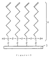
- Figure 5 shows a voltage-applying step in an example of the invention.
- the invention relates to an ultra thin polymer film electret and a method of manufacturing the same and aims to provide an electret, having the thickness of a molecular film, which has a sufficient surface elecric charge.
- a monomolecular film comprising an adsorptive reageant was formed on a substrate using trichlorosilane as an adsorptive reageant.
- an ultra thin polymer film electret was formed.
- An electret which has a high surface electric charge can be obtained by converting an ultra thin polymer film comprising high orientation into an electret.
- a chemical adsorption method or Langumuir-Blodgett's technique method is used as a step of forming the monomolecular film or a laminated film on a substrate surface.
- the LB method (Langmuir-Blodgett's technique) is used as a step of forming a pre-polymerized monomolecular film on a substrate surface.
- An adsorbing molecule which can be used for the chemical adsorption method comprises at least a functional group which reacts to an active hydrogen and a polymerized unsaturated group.
- a group having an active chloro group such as a chlorosilyl group, a chloro titanium group, a chloro stannyl group (where n represents 1 or 2 or 3 and X represents a substituted group such as a hydrogen atom or a lower alkyl group or a lower alkoxyl group) is used as a functional group.
- a vinylene group or an ethynylene group is used as a polymerized unsaturated group.
- Any substrate which has an active hydrogen such as -OH group, -COOH group, >NH group, -NH2 group on its surface can be used for the chemical adsorption method.
- glass such as quartz glass, fluoride glass, metalic glass and metalic materials such as aluminum, iron, stainless steel and titanium and semiconductor materials such as silicon and germanium is used as a substrate for the chemical adsorption method.
- a substrate which has few active hydrogens on its surface can be made into an appropriate substrate by increasing the numbers of active hydrogen on its surface by conventional chemical treatment such as by ozone oxidation or irraddiating it with an electron beam.
- a chemically adsorbed molecule can be used alone or it can be diluted with solvent.
- Any solvent which is a non-aqueous organic solvent containing as little moisture as possible to keep the chemically adsorbed molecule from reacting with the hydroxyl molecule and to not substantially corrode the substrate and to dissolve the adsorbing molecule sufficiently.
- organic solvents are long chain alkyl-based solvents, aromatic hydrocarbon-based solvents, aliphatic hydrocarbon-based solvents and halogen-containing solvents.
- a film is chemically bonded to a substrate and the thermomechanical stability of the film is increased and a substantialy pin-hole free film can be formed.
- the orientation of film molecules can be controlled and at the same time the film has a voltage-proof property and a high voltage can be applied to the film.
- an electret comprising a sufficient surface electric charge can be formed.
- a monomolecular film can be formed easily by washing with a non-aqueous organic solution such as chloroform to remove unreacted adsorbing molecule after the adsorption step.
- a monomolecular film or a monomolecular laminated film of an ultra thin polymer film electret is excellent for controlling the orientation of molecules. It is preferable in the invention to achieve an electret which has sufficient surface electric charge by controlling the orientation of the molecules.
- a molecule having ampohipathic character comprising a hydrophilic group and a hydrophobic group and comprising a polymerized group can be used for the LB method.
- the hydrophilic group are a carboxyl group (-COOH), a phosphoric acid group (-PO3 ), an amino group (-NH2 ).
- the ultra thin polymer film electret can be formed by the LB method.
- a thin polymerized film can be formed on a substrate by using a pre-polymerized polymer by addition condensation or condensation polymerization.
- Substrates which can be used for the LB method are substrates comprising an active hydrogen which is used for the above mentioned chemical adsorption method. In addition, any substrate comprising non active hydrogen can also be used.
- a solution which can be used for the LB method is changed by the molecules of the film. Mainly, water and salt, added at a controlled pH, are used.
- a monomolecular film or a laminated film by the LB method it is beneficial to be able to control the density and the condition of molecules in the film by controling the degree of polymerization. Further, it is beneficial to be able to use numerous kinds of molecules.
- a pre-polymerized monomolecular film by the LB method it is unnecessary to have a polymerization step after the film is formed. At the same time, in polymerizing the pre-formed monomolecular film or laminated film, it is beneficial that an adsorbing molecule is substantially free from elimination from a substrate.
- an energy beam which is used for polymerization depends on the molecules of the film. Particularly, it depends on the kinds and numbers of the polymerized unsaturated groups. Examples of those are X rays, electric beams, ultraviolet rays, and gamma rays.
- the strength of the energy beam also depends on the molecules of the film or the unsaturated groups.
- High voltage is applied to a film in order to provide a surface electric charge.
- the strength of the direct electric field depends on the molecules of the film. However, it is preferable to apply 104 to 107 V/cm.
- a monomolecular film or a laminated film which is formed by the above mentioned chemical adsorption method or the LB method, has high orientation at the molecular level as a chain portion of the polymer is filled densely on the surface substrate.
- an ultra thin polymer layer electret having a thickness on the molecular order, which has sufficient electric charge, can be formed.
- the chemical adsorption polymer film of the invention is ultra thin film, in the order of nanometers or Angstroms, it dose not spoil the characteristics of the substrate such as mechanical strength.
- Nonadecenyl trichlorosilane comprising a vinyl group as a polymerized unsaturated group was used as an adsorbing reagent 1. It was dissolved in a non-aqueous organic solvent 2 containing 10 mmol/L of nonadecenyl trichlorosilane.
- the non-aqueous organic solvent 2 contains 80 % by weight of normal hexadecane, 12 % by weight of chloroform and 8 % by weight of carbon tetrachloride.
- the substrate 3 was dipped and held in the solution at 30 °C to start the chemical adsorption reaction.
- An aluminum substrate was used in the example of the invention as substrate 3.
- the substrate 3 was dipped and held in the solution for about five hours and washed with a non-aqueous organic solution, followed by washing with pure water, thus, the monomolecular film 4 illustrated in Figure 3 was formed.
- a vinyl group was polymerized by irradiating the chemically adsorbed monomolecular film above with an electron beam 5 of about 5 Mrads in a vacuum atmosphere at normal temperature. According to an analysis of the pre-polymerized chemically adsorbed monomolecular film 4 and the polymerized film 6 by FT-IR, the vinyl group vanished after irradiating with the electron beam 5 and polymerization of the vinyl group was confirmed.
- the formed ultra thin polymer film electret had a surface electric charge of about 10 ⁇ 8 C/cm2 .
- the formation of chemicaly adsorbed polymer film was measured by FTIR.
- the thickness was about 2.3 nanometers (nm) by ESCA.
- nonadecenyl trichlorosilane was used as an adsorbing reagent.
- the ultra thin polymer film electret was formed by experiments with the same condition except using nonadecenyl methyldichlorosilane or nanadecenyl dimethylchlorosilane or nanadecenyl trichlorotitanium or nanadecenyl trichlorostannum was used as an adsorbing reagent.
- An aluminum substrate was dipped and held in the solution at 30 °C to start the chemical adsorption reaction for about five hours and washed with chloroform as in example 1, followed by washing with pure water.
- a substrate comprising the chemically adsorbed monomolecular film was dipped and held in a methanol solvent containing 2.5 % by weight of tetramethylammonium hydroxide solution for three hours.
- a methanol solvent containing 2.5 % by weight of tetramethylammonium hydroxide solution for three hours.
- the above mentioned chemical adsorption reaction was made to form a second layer molecular film and was, therefore, laminated.
- 10 layers of laminated film were formed.
- the vinyl groups were polymer by irradiating the thus formed laminated film with an electron beam of about 10 Mrads in a vacuum atomosphere at normal temperature. According to an analysis of the pre-polymerized laminated film and the laminated film by FT-IR, the vinyl group vanished and polymerization of the vinyl group was confirmed.
- a high electric field of 200 kV/cm at 120 °C was applied to the laminated film and an ultra thin polymer film electret was formed.
- ultra thin polymer film electret had about a 10 ⁇ 7 C/cm2 surface electric charge.
- the formation of chemicaly adsorbed polymer film was measured by FTIR.
- the thickness was about 25 nanometers (nm) by ESCA.
- polymerization was initiated after forming the laminated film.
- the same kind electret was formed after each film layer was adsorbed.
- An ultra thin polymer film electret was formed by applying a 200 kV/cm voltage to the monomolecular film.
- the ultra thin polymer film electret had about a 10 ⁇ 8 C/cm2 surface electric charge.
- the formation of physicaly adsorbed polymer film was measured by FTIR.
- the thickness was about 2.4 nanometers (nm) by ESCA.
- the formed electret had about 10 ⁇ 6 C/cm2 surface electric charge.
- the thickness was about 125 nanometers (nm) by ESCA.
- a diamine molecule shown in formula 2 or a diester molecule shown in formula 3 was used in making the ultra thin polymer film.
- the molecule was polymerized by condensation polymerization at 5mN/m of development solution comprising these molecules in a ratio of one to one.
- the polymerized film was formed on an aluminum substrate as a monomolecular film.
- An ultra thin polymer film electret was formed by applying a 200 kV/cm voltage to the monomolecular film.
- the formed ultra thin polymer film electret had about a 10 ⁇ 8 C/cm2 surface electric charge.
- the formation of physicaly adsorbed polymer film was measured by FTIR.
- the thickness was about 2.6 nanometers (nm) by ESCA.
- An electret having about a 10 ⁇ 8 C/cm2 surface electric charge was formed by irradiating a polytetrafluoroethylene film having a 10 ⁇ m thickness with an electron beam of 20 kV for several seconds at an electric current density of 0.05 ⁇ A/cm2 .
- the ultra thin polymer film electret had a thickness of about 1/1000 as that of prior electrets.
- the ultra thin polymer film electret of the invention had the same amount of surface electric charge as that of prior electrets.
- the laminated form of the ultra thin polymer film electret had a greater surface charge than that of prior electrets.
- the ultra thin polymer film electret in the example of the invention is put to practical use in the manufacture of super small-size microphones and speakers and motors. Further, the ultra thin polymer film electret in the invention is put to practical use in manufacturing small-size transformer devices utilizing electric proof property and artificial blood vessels in which blood is not substantially congelated.
- the invention is greatly beneficial to industry.
Applications Claiming Priority (2)
| Application Number | Priority Date | Filing Date | Title |
|---|---|---|---|
| JP3173615A JPH0517595A (ja) | 1991-07-15 | 1991-07-15 | 高分子超薄膜エレクトレツト及びその製造方法 |
| JP173615/91 | 1991-07-15 |
Publications (3)
| Publication Number | Publication Date |
|---|---|
| EP0523503A2 true EP0523503A2 (de) | 1993-01-20 |
| EP0523503A3 EP0523503A3 (de) | 1994-02-16 |
| EP0523503B1 EP0523503B1 (de) | 1997-10-08 |
Family
ID=15963899
Family Applications (1)
| Application Number | Title | Priority Date | Filing Date |
|---|---|---|---|
| EP92111440A Expired - Lifetime EP0523503B1 (de) | 1991-07-15 | 1992-07-06 | Ultradünner Polymerfilm-Elektret und Verfahren zu seiner Herstellung |
Country Status (4)
| Country | Link |
|---|---|
| US (2) | US5436033A (de) |
| EP (1) | EP0523503B1 (de) |
| JP (1) | JPH0517595A (de) |
| DE (1) | DE69222577T2 (de) |
Families Citing this family (18)
| Publication number | Priority date | Publication date | Assignee | Title |
|---|---|---|---|---|
| JPH0517595A (ja) * | 1991-07-15 | 1993-01-26 | Matsushita Electric Ind Co Ltd | 高分子超薄膜エレクトレツト及びその製造方法 |
| KR940004732A (ko) * | 1992-08-07 | 1994-03-15 | 가나이 쯔또무 | 패턴 형성 방법 및 패턴 형성에 사용하는 박막 형성 방법 |
| CA2124237C (en) | 1994-02-18 | 2004-11-02 | Bernard Cohen | Improved nonwoven barrier and method of making the same |
| CA2136576C (en) | 1994-06-27 | 2005-03-08 | Bernard Cohen | Improved nonwoven barrier and method of making the same |
| WO1996017569A2 (en) | 1994-12-08 | 1996-06-13 | Kimberly-Clark Worldwide, Inc. | Method of forming a particle size gradient in an absorbent article |
| CA2153278A1 (en) | 1994-12-30 | 1996-07-01 | Bernard Cohen | Nonwoven laminate barrier material |
| ZA965786B (en) | 1995-07-19 | 1997-01-27 | Kimberly Clark Co | Nonwoven barrier and method of making the same |
| US5834384A (en) | 1995-11-28 | 1998-11-10 | Kimberly-Clark Worldwide, Inc. | Nonwoven webs with one or more surface treatments |
| US6537932B1 (en) | 1997-10-31 | 2003-03-25 | Kimberly-Clark Worldwide, Inc. | Sterilization wrap, applications therefor, and method of sterilizing |
| US6037168A (en) * | 1997-12-31 | 2000-03-14 | Cytonix Corporation | Microbiological assembly comprising resealable closure means |
| US6365088B1 (en) | 1998-06-26 | 2002-04-02 | Kimberly-Clark Worldwide, Inc. | Electret treatment of high loft and low density nonwoven webs |
| US6068878A (en) | 1998-09-03 | 2000-05-30 | Micron Technology, Inc. | Methods of forming layers of particulates on substrates |
| US6621191B1 (en) * | 1999-05-13 | 2003-09-16 | Matsushita Electric Industrial Co., Inc. | Structure containing organic molecular layer and use thereof |
| NO312180B1 (no) * | 2000-02-29 | 2002-04-08 | Thin Film Electronics Asa | Fremgangsmåte til behandling av ultratynne filmer av karbonholdige materialer |
| WO2003062310A1 (en) * | 2002-01-23 | 2003-07-31 | Glasshield Patent Holding Company, Ltd. | Method and apparatus for applying material to glass |
| US20040254322A1 (en) * | 2003-06-10 | 2004-12-16 | Trent John S. | Easily torn charged or uncharged films and methods and compositions for producing same |
| KR100879279B1 (ko) | 2007-02-14 | 2009-01-16 | 이상열 | 고온용 일렉트릿트, 그의 제조방법 및 이를 구비하는마이크로폰 |
| WO2010131241A2 (en) * | 2009-05-13 | 2010-11-18 | Yevgeni Preezant | Improved photo-voltaic cell structure |
Citations (6)
| Publication number | Priority date | Publication date | Assignee | Title |
|---|---|---|---|---|
| FR2304629A1 (fr) * | 1975-03-20 | 1976-10-15 | Commissariat Energie Atomique | Materiau reticule, de structure organisee, sous forme de film ultra-mince |
| DE3039561A1 (de) * | 1979-10-19 | 1981-07-02 | Corporation de L'Ecole Polytechnique, Montreal, Quebec | Elektret und verfahren zu dessen herstellung sowie verwendung desselben |
| JPS62221103A (ja) * | 1986-03-24 | 1987-09-29 | 松下電器産業株式会社 | コンデンサ−およびその製造方法 |
| JPS6410611A (en) * | 1987-07-02 | 1989-01-13 | Marcon Electronics Co | Manufacture of capacitor |
| JPH01232038A (ja) * | 1988-03-11 | 1989-09-18 | Kuraray Co Ltd | エレクトレット化高分子シート状物及びその製造方法 |
| EP0452955A2 (de) * | 1990-04-20 | 1991-10-23 | Matsushita Electric Industrial Co., Ltd. | Kondensator und Verfahren zu seiner Herstellung |
Family Cites Families (14)
| Publication number | Priority date | Publication date | Assignee | Title |
|---|---|---|---|---|
| CA1107950A (en) * | 1978-08-10 | 1981-09-01 | Anupama Mishra | Electret made of branched alpha-olefin polymer |
| US4877988A (en) * | 1982-03-01 | 1989-10-31 | Battelle Memorial Institute | Piezoelectric and pyroelectric polymers |
| GB2136207B (en) * | 1983-03-07 | 1987-06-17 | Harold Wilson Meredith Pook | Manufacture of electrets |
| US4539061A (en) * | 1983-09-07 | 1985-09-03 | Yeda Research And Development Co., Ltd. | Process for the production of built-up films by the stepwise adsorption of individual monolayers |
| US4808849A (en) * | 1987-02-03 | 1989-02-28 | Canadian Patents And Development Limited/Societe Canadienne Des Brevets Et D'exploitation Limitee | Phyllosilicate electrets and a method for their manufacture |
| US4874399A (en) * | 1988-01-25 | 1989-10-17 | Minnesota Mining And Manufacturing Company | Electret filter made of fibers containing polypropylene and poly(4-methyl-1-pentene) |
| JP2672329B2 (ja) * | 1988-05-13 | 1997-11-05 | 東レ株式会社 | エレクトレット材料 |
| US5035782A (en) * | 1988-06-28 | 1991-07-30 | Matsushita Electric Industrial Co., Ltd. | Method for the formation of monomolecular adsorption films or built-up films of monomolecular layers using silane compounds having an acetylene or diacetylene bond |
| EP0385656B1 (de) * | 1989-02-27 | 1995-05-10 | Matsushita Electric Industrial Co., Ltd. | Verfahren zur Herstellung eines hoch orientierten ultralangen konjugierten Polymers |
| DE69127381T2 (de) * | 1990-01-19 | 1998-01-22 | Canon Kk | Informationsverarbeitungssystem und Informationsverarbeitungsmethode |
| DE69128160T2 (de) * | 1990-02-05 | 1998-03-26 | Matsushita Electric Ind Co Ltd | Verfahren zur Herstellung eines organischen monomolekularen Überzuges |
| US5061760A (en) * | 1990-03-09 | 1991-10-29 | Hoechst Celanese Corporation | Vinylidene cyanide alternating copolymers exhibiting nonlinear optical and piezoelectric properties |
| JPH0517595A (ja) * | 1991-07-15 | 1993-01-26 | Matsushita Electric Ind Co Ltd | 高分子超薄膜エレクトレツト及びその製造方法 |
| FI930259A (fi) * | 1992-11-06 | 1994-05-07 | Takiron Co | Polymert piezoelektriskt material |
-
1991
- 1991-07-15 JP JP3173615A patent/JPH0517595A/ja active Pending
-
1992
- 1992-07-06 EP EP92111440A patent/EP0523503B1/de not_active Expired - Lifetime
- 1992-07-06 DE DE69222577T patent/DE69222577T2/de not_active Expired - Fee Related
-
1994
- 1994-08-01 US US08/284,735 patent/US5436033A/en not_active Expired - Fee Related
-
1995
- 1995-07-25 US US08/507,667 patent/US5536982A/en not_active Expired - Lifetime
Patent Citations (6)
| Publication number | Priority date | Publication date | Assignee | Title |
|---|---|---|---|---|
| FR2304629A1 (fr) * | 1975-03-20 | 1976-10-15 | Commissariat Energie Atomique | Materiau reticule, de structure organisee, sous forme de film ultra-mince |
| DE3039561A1 (de) * | 1979-10-19 | 1981-07-02 | Corporation de L'Ecole Polytechnique, Montreal, Quebec | Elektret und verfahren zu dessen herstellung sowie verwendung desselben |
| JPS62221103A (ja) * | 1986-03-24 | 1987-09-29 | 松下電器産業株式会社 | コンデンサ−およびその製造方法 |
| JPS6410611A (en) * | 1987-07-02 | 1989-01-13 | Marcon Electronics Co | Manufacture of capacitor |
| JPH01232038A (ja) * | 1988-03-11 | 1989-09-18 | Kuraray Co Ltd | エレクトレット化高分子シート状物及びその製造方法 |
| EP0452955A2 (de) * | 1990-04-20 | 1991-10-23 | Matsushita Electric Industrial Co., Ltd. | Kondensator und Verfahren zu seiner Herstellung |
Non-Patent Citations (3)
| Title |
|---|
| DATABASE WPI Week 8744, Derwent Publications Ltd., London, GB; AN 87-311235 & JP-A-62 221 103 (MATSUSHITA ELEC IND KK) 29 September 1987 * |
| DATABASE WPI Week 8908, Derwent Publications Ltd., London, GB; AN 89-057910 & JP-A-1 010 611 (MARCON ELECTRONICS CO) 13 January 1989 * |
| DATABASE WPI Week 8943, Derwent Publications Ltd., London, GB; AN 89-313601 & JP-A-1 232 038 (KURARAY KK) 18 September 1989 * |
Also Published As
| Publication number | Publication date |
|---|---|
| US5436033A (en) | 1995-07-25 |
| EP0523503B1 (de) | 1997-10-08 |
| DE69222577T2 (de) | 1998-02-12 |
| US5536982A (en) | 1996-07-16 |
| DE69222577D1 (de) | 1997-11-13 |
| EP0523503A3 (de) | 1994-02-16 |
| JPH0517595A (ja) | 1993-01-26 |
Similar Documents
| Publication | Publication Date | Title |
|---|---|---|
| EP0523503A2 (de) | Ultradünner Polymerfilm-Elektret und Verfahren zu seiner Herstellung | |
| US5451459A (en) | Chemically absorbed film comprising fluorocarbon chains | |
| Rozsnyai et al. | Selective electrochemical deposition of polyaniline via photopatterning of a monolayer-modified substrate | |
| US5011518A (en) | Permselective membrane and process for producing the same | |
| EP0518219A2 (de) | Kondensator und Verfahren zu seiner Herstellung | |
| EP1551066A1 (de) | Material mit strukturoberfläche zur verwendung als vorlage und prozess seiner herstellung | |
| JPH0488678A (ja) | 有機デバイスとその製造方法 | |
| US5093154A (en) | Process for preparing a monomolecular built-up film | |
| JPH043907A (ja) | コンデンサーとその製造方法 | |
| EP0799688B1 (de) | Hydrophiler chemisch adsorbierter Film und Verfahren zu dessen Herstellung | |
| EP0312100B1 (de) | Verfahren zur Herstellung eines Polyacetylen- oder Polydiacetylenfilms | |
| US5695836A (en) | Antistatic film and method of manufacturing the same | |
| EP0344799B1 (de) | Selektiv-Permeabler Film und Verfahren zu seiner Herstellung | |
| US5019303A (en) | Process for producing polyacetylene | |
| JPH07104571B2 (ja) | 光記録媒体の製造方法 | |
| US5304583A (en) | Process for producing polyacetylene or polyacene type long conjugated polymers | |
| US5304582A (en) | Process for producing polyacetylene or polyacene type long conjugated polymers | |
| JPH02307572A (ja) | 均斉薄膜の形成方法 | |
| US5248526A (en) | Process for producing polyacetylene or polyacene type long conjugated polymers | |
| US5302416A (en) | Process for producing polyacetylene or polyacene type long conjugated polymers | |
| JPH0513530B2 (de) | ||
| JPH0627139B2 (ja) | ポリアセチレンの製造方法 | |
| JPH03229710A (ja) | 高配向性共役ポリマーの製造方法 | |
| JPH0247108A (ja) | ポリアセチレンの製造方法 | |
| JPH0748490B2 (ja) | 単分子累積膜形成方法 |
Legal Events
| Date | Code | Title | Description |
|---|---|---|---|
| PUAI | Public reference made under article 153(3) epc to a published international application that has entered the european phase |
Free format text: ORIGINAL CODE: 0009012 |
|
| AK | Designated contracting states |
Kind code of ref document: A2 Designated state(s): DE FR GB |
|
| PUAL | Search report despatched |
Free format text: ORIGINAL CODE: 0009013 |
|
| AK | Designated contracting states |
Kind code of ref document: A3 Designated state(s): DE FR GB |
|
| 17P | Request for examination filed |
Effective date: 19940223 |
|
| 17Q | First examination report despatched |
Effective date: 19950130 |
|
| GRAG | Despatch of communication of intention to grant |
Free format text: ORIGINAL CODE: EPIDOS AGRA |
|
| GRAH | Despatch of communication of intention to grant a patent |
Free format text: ORIGINAL CODE: EPIDOS IGRA |
|
| GRAH | Despatch of communication of intention to grant a patent |
Free format text: ORIGINAL CODE: EPIDOS IGRA |
|
| GRAA | (expected) grant |
Free format text: ORIGINAL CODE: 0009210 |
|
| AK | Designated contracting states |
Kind code of ref document: B1 Designated state(s): DE FR GB |
|
| REF | Corresponds to: |
Ref document number: 69222577 Country of ref document: DE Date of ref document: 19971113 |
|
| ET | Fr: translation filed | ||
| PLBE | No opposition filed within time limit |
Free format text: ORIGINAL CODE: 0009261 |
|
| STAA | Information on the status of an ep patent application or granted ep patent |
Free format text: STATUS: NO OPPOSITION FILED WITHIN TIME LIMIT |
|
| 26N | No opposition filed | ||
| REG | Reference to a national code |
Ref country code: GB Ref legal event code: IF02 |
|
| PGFP | Annual fee paid to national office [announced via postgrant information from national office to epo] |
Ref country code: DE Payment date: 20060629 Year of fee payment: 15 |
|
| PGFP | Annual fee paid to national office [announced via postgrant information from national office to epo] |
Ref country code: GB Payment date: 20060705 Year of fee payment: 15 |
|
| PGFP | Annual fee paid to national office [announced via postgrant information from national office to epo] |
Ref country code: FR Payment date: 20060719 Year of fee payment: 15 |
|
| GBPC | Gb: european patent ceased through non-payment of renewal fee |
Effective date: 20070706 |
|
| PG25 | Lapsed in a contracting state [announced via postgrant information from national office to epo] |
Ref country code: DE Free format text: LAPSE BECAUSE OF NON-PAYMENT OF DUE FEES Effective date: 20080201 |
|
| PG25 | Lapsed in a contracting state [announced via postgrant information from national office to epo] |
Ref country code: GB Free format text: LAPSE BECAUSE OF NON-PAYMENT OF DUE FEES Effective date: 20070706 |
|
| REG | Reference to a national code |
Ref country code: FR Ref legal event code: ST Effective date: 20080331 |
|
| PG25 | Lapsed in a contracting state [announced via postgrant information from national office to epo] |
Ref country code: FR Free format text: LAPSE BECAUSE OF NON-PAYMENT OF DUE FEES Effective date: 20070731 |