EP0312100B1 - Verfahren zur Herstellung eines Polyacetylen- oder Polydiacetylenfilms - Google Patents
Verfahren zur Herstellung eines Polyacetylen- oder Polydiacetylenfilms Download PDFInfo
- Publication number
- EP0312100B1 EP0312100B1 EP88117139A EP88117139A EP0312100B1 EP 0312100 B1 EP0312100 B1 EP 0312100B1 EP 88117139 A EP88117139 A EP 88117139A EP 88117139 A EP88117139 A EP 88117139A EP 0312100 B1 EP0312100 B1 EP 0312100B1
- Authority
- EP
- European Patent Office
- Prior art keywords
- group
- producing
- chain
- polyacetylene
- straight
- Prior art date
- Legal status (The legal status is an assumption and is not a legal conclusion. Google has not performed a legal analysis and makes no representation as to the accuracy of the status listed.)
- Expired - Lifetime
Links
- HSFWRNGVRCDJHI-UHFFFAOYSA-N alpha-acetylene Natural products C#C HSFWRNGVRCDJHI-UHFFFAOYSA-N 0.000 title claims description 31
- 238000000034 method Methods 0.000 title claims description 30
- 229920001197 polyacetylene Polymers 0.000 title claims description 30
- 229920000015 polydiacetylene Polymers 0.000 title claims description 18
- 150000002430 hydrocarbons Chemical class 0.000 claims description 29
- 239000004215 Carbon black (E152) Substances 0.000 claims description 20
- 229930195733 hydrocarbon Natural products 0.000 claims description 20
- 239000000758 substrate Substances 0.000 claims description 19
- 125000004432 carbon atom Chemical group C* 0.000 claims description 11
- KOPOQZFJUQMUML-UHFFFAOYSA-N chlorosilane Chemical group Cl[SiH3] KOPOQZFJUQMUML-UHFFFAOYSA-N 0.000 claims description 10
- LLCSWKVOHICRDD-UHFFFAOYSA-N buta-1,3-diyne Chemical group C#CC#C LLCSWKVOHICRDD-UHFFFAOYSA-N 0.000 claims description 9
- 150000001875 compounds Chemical class 0.000 claims description 9
- 125000002534 ethynyl group Chemical group [H]C#C* 0.000 claims description 9
- 125000000391 vinyl group Chemical group [H]C([*])=C([H])[H] 0.000 claims description 8
- 239000000126 substance Substances 0.000 claims description 6
- 238000001179 sorption measurement Methods 0.000 claims description 4
- 239000011356 non-aqueous organic solvent Substances 0.000 claims description 3
- 230000000379 polymerizing effect Effects 0.000 claims description 3
- 230000005660 hydrophilic surface Effects 0.000 claims description 2
- 238000010884 ion-beam technique Methods 0.000 claims 1
- 229910052799 carbon Inorganic materials 0.000 description 9
- 125000000524 functional group Chemical group 0.000 description 9
- VYPSYNLAJGMNEJ-UHFFFAOYSA-N Silicium dioxide Chemical compound O=[Si]=O VYPSYNLAJGMNEJ-UHFFFAOYSA-N 0.000 description 8
- 239000004094 surface-active agent Substances 0.000 description 7
- 150000000475 acetylene derivatives Chemical class 0.000 description 6
- BLRPTPMANUNPDV-UHFFFAOYSA-N Silane Chemical compound [SiH4] BLRPTPMANUNPDV-UHFFFAOYSA-N 0.000 description 5
- 230000015572 biosynthetic process Effects 0.000 description 5
- 238000006116 polymerization reaction Methods 0.000 description 5
- 229910000077 silane Inorganic materials 0.000 description 5
- 229910052681 coesite Inorganic materials 0.000 description 4
- 229910052906 cristobalite Inorganic materials 0.000 description 4
- 125000002887 hydroxy group Chemical group [H]O* 0.000 description 4
- 238000004519 manufacturing process Methods 0.000 description 4
- 239000000377 silicon dioxide Substances 0.000 description 4
- 235000012239 silicon dioxide Nutrition 0.000 description 4
- 229910052682 stishovite Inorganic materials 0.000 description 4
- 229910052905 tridymite Inorganic materials 0.000 description 4
- 239000012298 atmosphere Substances 0.000 description 3
- QVGXLLKOCUKJST-UHFFFAOYSA-N atomic oxygen Chemical compound [O] QVGXLLKOCUKJST-UHFFFAOYSA-N 0.000 description 3
- 125000002496 methyl group Chemical group [H]C([H])([H])* 0.000 description 3
- 230000003287 optical effect Effects 0.000 description 3
- 229910052760 oxygen Inorganic materials 0.000 description 3
- 239000001301 oxygen Substances 0.000 description 3
- 229920000642 polymer Polymers 0.000 description 3
- 238000001074 Langmuir--Blodgett assembly Methods 0.000 description 2
- 125000004429 atom Chemical group 0.000 description 2
- 238000006243 chemical reaction Methods 0.000 description 2
- 238000010894 electron beam technology Methods 0.000 description 2
- 230000001678 irradiating effect Effects 0.000 description 2
- 230000005855 radiation Effects 0.000 description 2
- XLYOFNOQVPJJNP-UHFFFAOYSA-N water Substances O XLYOFNOQVPJJNP-UHFFFAOYSA-N 0.000 description 2
- 239000011954 Ziegler–Natta catalyst Substances 0.000 description 1
- 125000001165 hydrophobic group Chemical group 0.000 description 1
- 239000000463 material Substances 0.000 description 1
- 239000008204 material by function Substances 0.000 description 1
- 239000000178 monomer Substances 0.000 description 1
- 125000004430 oxygen atom Chemical group O* 0.000 description 1
- 125000000843 phenylene group Chemical group C1(=C(C=CC=C1)*)* 0.000 description 1
- 125000000168 pyrrolyl group Chemical group 0.000 description 1
- 230000009257 reactivity Effects 0.000 description 1
- 230000006641 stabilisation Effects 0.000 description 1
- 238000011105 stabilization Methods 0.000 description 1
- 230000000087 stabilizing effect Effects 0.000 description 1
- 125000005556 thienylene group Chemical group 0.000 description 1
Images

Classifications
-
- B—PERFORMING OPERATIONS; TRANSPORTING
- B05—SPRAYING OR ATOMISING IN GENERAL; APPLYING FLUENT MATERIALS TO SURFACES, IN GENERAL
- B05D—PROCESSES FOR APPLYING FLUENT MATERIALS TO SURFACES, IN GENERAL
- B05D1/00—Processes for applying liquids or other fluent materials
- B05D1/18—Processes for applying liquids or other fluent materials performed by dipping
- B05D1/185—Processes for applying liquids or other fluent materials performed by dipping applying monomolecular layers
-
- B—PERFORMING OPERATIONS; TRANSPORTING
- B82—NANOTECHNOLOGY
- B82Y—SPECIFIC USES OR APPLICATIONS OF NANOSTRUCTURES; MEASUREMENT OR ANALYSIS OF NANOSTRUCTURES; MANUFACTURE OR TREATMENT OF NANOSTRUCTURES
- B82Y10/00—Nanotechnology for information processing, storage or transmission, e.g. quantum computing or single electron logic
-
- B—PERFORMING OPERATIONS; TRANSPORTING
- B82—NANOTECHNOLOGY
- B82Y—SPECIFIC USES OR APPLICATIONS OF NANOSTRUCTURES; MEASUREMENT OR ANALYSIS OF NANOSTRUCTURES; MANUFACTURE OR TREATMENT OF NANOSTRUCTURES
- B82Y20/00—Nanooptics, e.g. quantum optics or photonic crystals
-
- B—PERFORMING OPERATIONS; TRANSPORTING
- B82—NANOTECHNOLOGY
- B82Y—SPECIFIC USES OR APPLICATIONS OF NANOSTRUCTURES; MEASUREMENT OR ANALYSIS OF NANOSTRUCTURES; MANUFACTURE OR TREATMENT OF NANOSTRUCTURES
- B82Y30/00—Nanotechnology for materials or surface science, e.g. nanocomposites
-
- B—PERFORMING OPERATIONS; TRANSPORTING
- B82—NANOTECHNOLOGY
- B82Y—SPECIFIC USES OR APPLICATIONS OF NANOSTRUCTURES; MEASUREMENT OR ANALYSIS OF NANOSTRUCTURES; MANUFACTURE OR TREATMENT OF NANOSTRUCTURES
- B82Y40/00—Manufacture or treatment of nanostructures
-
- C—CHEMISTRY; METALLURGY
- C08—ORGANIC MACROMOLECULAR COMPOUNDS; THEIR PREPARATION OR CHEMICAL WORKING-UP; COMPOSITIONS BASED THEREON
- C08F—MACROMOLECULAR COMPOUNDS OBTAINED BY REACTIONS ONLY INVOLVING CARBON-TO-CARBON UNSATURATED BONDS
- C08F138/00—Homopolymers of compounds having one or more carbon-to-carbon triple bonds
-
- G—PHYSICS
- G02—OPTICS
- G02F—OPTICAL DEVICES OR ARRANGEMENTS FOR THE CONTROL OF LIGHT BY MODIFICATION OF THE OPTICAL PROPERTIES OF THE MEDIA OF THE ELEMENTS INVOLVED THEREIN; NON-LINEAR OPTICS; FREQUENCY-CHANGING OF LIGHT; OPTICAL LOGIC ELEMENTS; OPTICAL ANALOGUE/DIGITAL CONVERTERS
- G02F1/00—Devices or arrangements for the control of the intensity, colour, phase, polarisation or direction of light arriving from an independent light source, e.g. switching, gating or modulating; Non-linear optics
- G02F1/35—Non-linear optics
- G02F1/355—Non-linear optics characterised by the materials used
- G02F1/361—Organic materials
- G02F1/3615—Organic materials containing polymers
-
- G—PHYSICS
- G02—OPTICS
- G02F—OPTICAL DEVICES OR ARRANGEMENTS FOR THE CONTROL OF LIGHT BY MODIFICATION OF THE OPTICAL PROPERTIES OF THE MEDIA OF THE ELEMENTS INVOLVED THEREIN; NON-LINEAR OPTICS; FREQUENCY-CHANGING OF LIGHT; OPTICAL LOGIC ELEMENTS; OPTICAL ANALOGUE/DIGITAL CONVERTERS
- G02F1/00—Devices or arrangements for the control of the intensity, colour, phase, polarisation or direction of light arriving from an independent light source, e.g. switching, gating or modulating; Non-linear optics
- G02F1/35—Non-linear optics
- G02F1/355—Non-linear optics characterised by the materials used
- G02F1/361—Organic materials
- G02F1/3618—Langmuir Blodgett Films
-
- H—ELECTRICITY
- H01—ELECTRIC ELEMENTS
- H01L—SEMICONDUCTOR DEVICES NOT COVERED BY CLASS H10
- H01L21/00—Processes or apparatus adapted for the manufacture or treatment of semiconductor or solid state devices or of parts thereof
- H01L21/02—Manufacture or treatment of semiconductor devices or of parts thereof
- H01L21/04—Manufacture or treatment of semiconductor devices or of parts thereof the devices having potential barriers, e.g. a PN junction, depletion layer or carrier concentration layer
- H01L21/18—Manufacture or treatment of semiconductor devices or of parts thereof the devices having potential barriers, e.g. a PN junction, depletion layer or carrier concentration layer the devices having semiconductor bodies comprising elements of Group IV of the Periodic Table or AIIIBV compounds with or without impurities, e.g. doping materials
- H01L21/30—Treatment of semiconductor bodies using processes or apparatus not provided for in groups H01L21/20 - H01L21/26
- H01L21/31—Treatment of semiconductor bodies using processes or apparatus not provided for in groups H01L21/20 - H01L21/26 to form insulating layers thereon, e.g. for masking or by using photolithographic techniques; After treatment of these layers; Selection of materials for these layers
- H01L21/3205—Deposition of non-insulating-, e.g. conductive- or resistive-, layers on insulating layers; After-treatment of these layers
- H01L21/32056—Deposition of conductive or semi-conductive organic layers
-
- H—ELECTRICITY
- H10—SEMICONDUCTOR DEVICES; ELECTRIC SOLID-STATE DEVICES NOT OTHERWISE PROVIDED FOR
- H10K—ORGANIC ELECTRIC SOLID-STATE DEVICES
- H10K85/00—Organic materials used in the body or electrodes of devices covered by this subclass
- H10K85/10—Organic polymers or oligomers
- H10K85/141—Organic polymers or oligomers comprising aliphatic or olefinic chains, e.g. poly N-vinylcarbazol, PVC or PTFE
- H10K85/143—Polyacetylene; Derivatives thereof
-
- H—ELECTRICITY
- H10—SEMICONDUCTOR DEVICES; ELECTRIC SOLID-STATE DEVICES NOT OTHERWISE PROVIDED FOR
- H10K—ORGANIC ELECTRIC SOLID-STATE DEVICES
- H10K85/00—Organic materials used in the body or electrodes of devices covered by this subclass
- H10K85/40—Organosilicon compounds, e.g. TIPS pentacene
-
- H—ELECTRICITY
- H10—SEMICONDUCTOR DEVICES; ELECTRIC SOLID-STATE DEVICES NOT OTHERWISE PROVIDED FOR
- H10K—ORGANIC ELECTRIC SOLID-STATE DEVICES
- H10K85/00—Organic materials used in the body or electrodes of devices covered by this subclass
- H10K85/701—Langmuir Blodgett films
Definitions
- Polymers of acetylene derivatives have been extensively studied as optical and electronic functional materials because they have electrical conductivity and nonlinear optical effect by virtue of the primary main chain having a ⁇ -electron conjugated system which is contained in the molecule of each polymer.
- LB Langmuir-Blodgett
- polyacetylene derivatives now known are unstable to heat, pressure, ultraviolet rays, etc. in an atmosphere containing oxygen, and therefore study of their stabilization is in progress.
- From EP 0 178 606 is known a process for producing a polyacetylene film on a substrate, comprising immersing the substrate having a hydrophilic OH-groups containing surface in a solution of a straight-chain hydrocarbon compound having a chlorosilane group on one end of the hydrocarbon chain and one or more groups being reactive to energy beams (e.g.
- acetylene or diacetylene at an optional position in the hydrocarbon chain, in a nonaqueous organic solvent, and thereby subjecting the chlorosilane group of the compound and the OH-group on the surface of the substrate to a chemical reaction, whereby a monomolecular film of the reacted compound is formed in the substrate, and polymerizing the molecules of the compound by irradiation with energy beams.
- a process for producing a polyacetylene or a polydiacetylene film comprising immersing a substrate having a hydrophilic surface in a solution of a straight-chain hydrocarbon compound having a chlorosilane group on one end of the hydrocarbon chain and one or more groups being reactive to energy beams at an optional position in the hydrocarbon chain, in a nonaqueous organic solvent, and thereby subjecting the chlorosilane group of the compound to chemical adsorption on the surface of the substrate, whereby a monomolecular film of the compound is formed on the substrate, and polymerizing the molecules of the compound by irradiation with energy beams, wherein said straight-chain hydrocarbon molecule forming a main chain has one or more side chains, and said group(s) reactive to energy beams are present in the main chain and in one or more side chains of said main chain.
- a monomolecular film is formed by using straight-chain hydrocarbon molecules having one or more side chains in optional positions of the molecules and reactive groups to impart a function in the main chain and the side chain, and then subjected to polymerization by irradiating the reactive groups with energy beams, and if necessary, the films subjected to polymerization are formed into a multilayer film, whereby there is solved the conventional problem that since the end of a straight-chain hydrocarbon molecular chain contains oxygen as shown by -Si-O-Si- and the straight-chain hydrocarbon molecule has no side chain, functional groups of the molecule are too apart to react with each other. Thus, the distance between the functional groups is reduced, so that their reactivity can be enhanced, and moreover occurrence or a structural distortion is reduced.
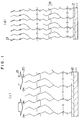
- Numeral 11 shows an optional substrate (e.g., a Si substrate) for forming a polyacetylene.
- Numeral 12 shows a hydrophilic film (e.g., a SiO2 film) formed on the optional substrate 1.
- Numeral 13 shows a silane surfactant of the formula: (wherein each of p, g, r, s and t is an optional integer), said silane surfactant constituting a monomolecular film 16 comprising straight-chain hydrocarbon molecules which have a side chain at the (r+1)th carbon atom from the Si atom, an acetylene group (-C ⁇ C-) 14 as functional group at the (q+1)th carbon atoms of the main chain from said (r+1)th carbon atom, an acetylene group 14' at the (t+1)th carbon atom of the side chain from said (r+1)th carbon atom, and a vinyl group at the end of the main chain.
- the terminal group on the Si side in the above chemical formula is a chlorosilane group (-SiCl3).
- the linkage is formed on the surface of the hydrophilic film (e.g., SiO2 film) 12 by a monomolecular film forming method such as chemical adsorption method or Langmuir-Blodgett technique, whereby the monomolecular film 16 is formed.
- This polyacetylene has electrical conductivity and nonlinear optical effect, can be utilized as a photoelectronic functional material, and can be shaped in an optional direction on the same plane.
- the film is irradiated in a water vapor atmosphere with energy beams, for example, electron beams converged to the molecular diameter order to activate the aforesaid vinyl group, whereby a hydroxyl group 20 is added thereto (Fig. 1(c)).
- energy beams for example, electron beams converged to the molecular diameter order to activate the aforesaid vinyl group, whereby a hydroxyl group 20 is added thereto (Fig. 1(c)).
- the same silane surfactant as the aforesaid surfactant 13, i.e., (wherein each of p, q, r, s and t is an optional integer) is added to the active group portion having a hydroxyl group added thereto, in the same manner as described above to form the linkage
- vinyl groups 21 are aligned on the surface of the added molecule, a higher-order multilayer molecular structure is formed, namely, polyacetylene can be formed (Fig. 1(b)).
- silane surfactant having one side chain of the formula: (wherein each p, q, r, s and t is an optional integer), the number of side chains may be increased if necessary.
- radiation such as X-rays, electron beams, etc. may be used for the polymerization.
- terminal group of the side chain is a methyl group in the first example of the present invention, it may be replaced by a vinyl group.
- diacetylene group is shown as a functional group in the first example of the present invention, other functional groups such as pyrrole group, thienylene group, phenylene group, etc. may, of course, be employed.
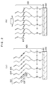
- Numeral 100 shows an optional substrate (e.g., a Si substrate) for producing a polydiacetylene.
- Numeral 101 shows a hydrophilic film (e.g., a SiO2 film) formed on the optional substrate 100.
- Numeral 102 shows a silane surfactant of the formula: (wherein each of p, q, r, s and t is an optional integer), said surfactant constituting a monomolecular film 105 comprising straight-chain hydrocarbon molecules which have a side chain at the (r+1)th carbon atom from the Si atom, a diacetylene group (-C ⁇ C-C ⁇ C-) 103 as functional group at the (q+1)th carbon atom of the main chain from said (r+1)th carbon atom, a diacetylene group 103' at the (t+1)th carbon atom of the side chain from said (r+1)th carbon atom, and a vinyl group 104 at the end of the main chain.
- the terminal group on the Si side in the above chemical formula is a chlorosilane group (-SiCl3).
- This polydiacetylene has electrical conductivity, is expected to be utilized as a molecular wiring, and can be shaped in an optional direction on the same plane.
- a polyacetylene can be produced also according to the second example.
- the difference between processes for production of a polydiacetylene and a polyacetylene is due to the density of diacetylene groups in the main chain and the side chain of a straight-chain hydrocarbon molecule and the uprightness of the straight-chain hydrocarbon molecules. That is, when the density of diacetylene groups is high and the straight-chain hydrocarbon molecules are upright, a polyacetylene is formed, and when the molecules are in a relatively inclined state, a polydiacetylene is formed (Fig. 2(b)).
- a multilayer structure of polydiacetylene can be formed by the same manner as described in the first example.
- a functional portion such as polyacetylene, polydiacetylene or the like may be combined with each layer.
Landscapes
- Engineering & Computer Science (AREA)
- Chemical & Material Sciences (AREA)
- Physics & Mathematics (AREA)
- Nanotechnology (AREA)
- Nonlinear Science (AREA)
- General Physics & Mathematics (AREA)
- Crystallography & Structural Chemistry (AREA)
- Materials Engineering (AREA)
- Condensed Matter Physics & Semiconductors (AREA)
- Optics & Photonics (AREA)
- Manufacturing & Machinery (AREA)
- Theoretical Computer Science (AREA)
- Medicinal Chemistry (AREA)
- Biophysics (AREA)
- Composite Materials (AREA)
- Life Sciences & Earth Sciences (AREA)
- Health & Medical Sciences (AREA)
- Chemical Kinetics & Catalysis (AREA)
- Mathematical Physics (AREA)
- Polymers & Plastics (AREA)
- Organic Chemistry (AREA)
- Computer Hardware Design (AREA)
- Microelectronics & Electronic Packaging (AREA)
- Power Engineering (AREA)
- Addition Polymer Or Copolymer, Post-Treatments, Or Chemical Modifications (AREA)
- Manufacture Of Macromolecular Shaped Articles (AREA)
Claims (7)
- Verfahren zur Herstellung einer Polyacethylenschicht oder einer Polydiacethylenschicht mit- Eintauchen eines Trägers mit einer hydrophilen Oberfläche in eine Lösung einer gradkettigen Kohlenwasserstoffverbindung mit einer Chlorosilangruppe an einem Ende der Kohlenwasserstoffkette und einer oder mehreren auf Energiestrahlen reagierenden Gruppen an wählbaren Stellen in der Kohlenwasserstoffkette in einem nicht wässrigen organischen Lösungsmittel und dadurch Unterziehen der Chlorosilangruppe der Verbindung einer chemischen Adsorption an der Oberfläche des Trägers, wodurch eine monomolekulare Schicht der Verbindung auf dem Träger gebildet wird, und- Polymerisieren der Moleküle der Verbindung durch Bestrahlung mit Energiestrahlen,
dadurch gekennzeichnet, daß- das eine Hauptkette bildende gradkettige Kohlenwasserstoffmolekül eine oder mehrere Seitenketten aufweist und- die auf Energiestrahlen reagierende(n) Gruppe(n) in der Hauptkette und in einer oder mehreren Seitenketten der Hauptkette vorliegenden. - Verfahren zur Herstellung einer Polyacethylenschicht nach Anspruch 1, bei dem die reaktive(n) Gruppe (n) eine Acethylengruppe oder eine Diacethylengruppe ist/sind.
- Verfahren zur Herstellung einer Polyacethylenschicht nach Anspruch 1 oder 2, bei dem die Energiestrahlen ultraviolette Strahlen, fernultraviolette Strahlen, Elektronen-Ionen-Strahlen, Röntgenstrahlen oder Gammastrahlen sind.
- Verfahren zur Herstellung einer Polyacethylenschicht nach einem der Ansprüche 1 bis 3, bei dem die Anzahl der das gradkettige Kohlenwasserstoffmolekül bildenden Kohlenstoffatome 10 oder mehr beträgt.
- Verfahren zur Herstellung einer Polyacethylenschicht nach einem der Ansprüche 1 bis 4, bei dem diejenige Endgruppe des gradkettigen Kohlenwasserstoffmoleküls, die nicht die Chlorosilanendgruppe ist, eine ungesättigte Gruppe ist.
- Verfahren zur Herstellung einer Polyacethylenschicht nach Anspruch 5, bei dem unter Verwendung der gradkettigen Kohlenwasserstoffmoleküle mit der ungesättigten Gruppe eine mehrlagige Schicht gebildet wird.
- Verfahren zur Herstellung einer Polyacethylenschicht nach Anspruch 6, bei der die ungesättigte Gruppe eine Vinylgruppe ist.
Applications Claiming Priority (4)
| Application Number | Priority Date | Filing Date | Title |
|---|---|---|---|
| JP262043/87 | 1987-10-16 | ||
| JP26204387A JPH0627139B2 (ja) | 1987-10-16 | 1987-10-16 | ポリアセチレンの製造方法 |
| JP62309054A JPH0735413B2 (ja) | 1987-12-07 | 1987-12-07 | ポリアセチレンまたはポリジアセチレンの形成方法 |
| JP309054/87 | 1987-12-07 |
Publications (3)
| Publication Number | Publication Date |
|---|---|
| EP0312100A2 EP0312100A2 (de) | 1989-04-19 |
| EP0312100A3 EP0312100A3 (en) | 1989-07-26 |
| EP0312100B1 true EP0312100B1 (de) | 1993-08-04 |
Family
ID=26545360
Family Applications (1)
| Application Number | Title | Priority Date | Filing Date |
|---|---|---|---|
| EP88117139A Expired - Lifetime EP0312100B1 (de) | 1987-10-16 | 1988-10-14 | Verfahren zur Herstellung eines Polyacetylen- oder Polydiacetylenfilms |
Country Status (3)
| Country | Link |
|---|---|
| US (1) | US4968524A (de) |
| EP (1) | EP0312100B1 (de) |
| DE (1) | DE3882881T2 (de) |
Families Citing this family (12)
| Publication number | Priority date | Publication date | Assignee | Title |
|---|---|---|---|---|
| JPH0626706B2 (ja) * | 1988-09-05 | 1994-04-13 | 日本原子力研究所 | 単分子累積膜の製造方法 |
| US5260115A (en) * | 1989-02-15 | 1993-11-09 | Matsushita Electric Industrial Co., Ltd. | Organic electro-conductive thin films and process for production thereof |
| JPH07103190B2 (ja) * | 1989-02-15 | 1995-11-08 | 松下電器産業株式会社 | 有機導電性薄膜とその製造方法 |
| US5204126A (en) * | 1990-02-06 | 1993-04-20 | Nanofilm Corporation | Mold surfaces with ultra thin release films |
| JP2649856B2 (ja) * | 1990-04-13 | 1997-09-03 | 松下電器産業株式会社 | 非線形光学材料 |
| DE69121658T2 (de) * | 1990-09-17 | 1997-01-23 | Matsushita Electric Ind Co Ltd | Flüssigkristallorientierungsschicht und ihr Herstellungsverfahren |
| US5256456A (en) * | 1990-09-17 | 1993-10-26 | Matsushita Electric Industrial Co., Ltd. | Liquid crystal alignment film and method of manufacturing the same |
| IL98753A0 (en) * | 1990-10-10 | 1992-07-15 | Yeda Res & Dev | Process for the production of composite organic-inorganic superlattices |
| EP0499977B1 (de) * | 1991-02-19 | 1995-12-20 | Matsushita Electric Industrial Co., Ltd. | Verfahren zur Herstellung eines chemisch absorbierten Films |
| US5455072A (en) * | 1992-11-18 | 1995-10-03 | Bension; Rouvain M. | Initiation and bonding of diamond and other thin films |
| US5578351A (en) * | 1995-01-20 | 1996-11-26 | Geo-Centers, Inc. | Liquid crystal composition and alignment layer |
| WO1997007429A1 (en) * | 1995-08-18 | 1997-02-27 | President And Fellows Of Harvard College | Self-assembled monolayer directed patterning of surfaces |
Family Cites Families (5)
| Publication number | Priority date | Publication date | Assignee | Title |
|---|---|---|---|---|
| US4169904A (en) * | 1978-01-05 | 1979-10-02 | International Business Machines Corporation | Preparation of polymer monomolecular films |
| US4751171A (en) * | 1984-07-03 | 1988-06-14 | Matsushita Electric Industrial Co., Ltd. | Pattern forming method |
| JPS6194042A (ja) * | 1984-10-16 | 1986-05-12 | Matsushita Electric Ind Co Ltd | 分子構築体およびその製造方法 |
| JPS61134345A (ja) * | 1984-12-05 | 1986-06-21 | Kanegafuchi Chem Ind Co Ltd | ベンゼン環を含んだ両親媒性ジアセチレン化合物およびその膜 |
| GB8432406D0 (en) * | 1984-12-21 | 1985-02-06 | Gen Electric Co Plc | Stabilised langmuir-blodgett films |
-
1988
- 1988-10-12 US US07/256,619 patent/US4968524A/en not_active Expired - Lifetime
- 1988-10-14 DE DE88117139T patent/DE3882881T2/de not_active Expired - Fee Related
- 1988-10-14 EP EP88117139A patent/EP0312100B1/de not_active Expired - Lifetime
Also Published As
| Publication number | Publication date |
|---|---|
| EP0312100A2 (de) | 1989-04-19 |
| EP0312100A3 (en) | 1989-07-26 |
| US4968524A (en) | 1990-11-06 |
| DE3882881D1 (de) | 1993-09-09 |
| DE3882881T2 (de) | 1994-02-10 |
Similar Documents
| Publication | Publication Date | Title |
|---|---|---|
| US5057339A (en) | Metallized polyacetylene-type or polyacene-type ultralong conjugated polymers and process for producing the same | |
| EP0312100B1 (de) | Verfahren zur Herstellung eines Polyacetylen- oder Polydiacetylenfilms | |
| US5011518A (en) | Permselective membrane and process for producing the same | |
| US5008127A (en) | Process for the production of a highly-orientated ultralong conjugated polymer | |
| Hong et al. | Synthesis of electrically conductive polypyrroles at the air-water interface of a Langmuir-Blodgett film balance | |
| EP0178606B1 (de) | Struktur mit kontrolliertem Molekül und Verfahren zu deren Herstellung | |
| EP0523503B1 (de) | Ultradünner Polymerfilm-Elektret und Verfahren zu seiner Herstellung | |
| JPH08846B2 (ja) | ポリアセチレン型共役ポリマーの製造方法 | |
| EP0351092B1 (de) | Verfahren zur Herstellung von monomolekularen Adsorptionsfilmen oder aus monomolekularen Schichten aufgebauten Filmen unter Anwendung von Silanen, die Acetylen- oder Diacetylenbindungen enthalten | |
| JP3147407B2 (ja) | 導電性高分子複合材料およびその製造方法 | |
| US5093154A (en) | Process for preparing a monomolecular built-up film | |
| EP0339677B1 (de) | Verfahren zur Erzeugung von Polyazetylen oder Polyazen konjugierten Polymeren mit sehr langer Kette | |
| EP0341697B1 (de) | Verfahren zur Herstellung von Polyacetylen | |
| EP0344799B1 (de) | Selektiv-Permeabler Film und Verfahren zu seiner Herstellung | |
| US5304583A (en) | Process for producing polyacetylene or polyacene type long conjugated polymers | |
| US5304582A (en) | Process for producing polyacetylene or polyacene type long conjugated polymers | |
| JPH07104571B2 (ja) | 光記録媒体の製造方法 | |
| JPH0627139B2 (ja) | ポリアセチレンの製造方法 | |
| US5248526A (en) | Process for producing polyacetylene or polyacene type long conjugated polymers | |
| US5302416A (en) | Process for producing polyacetylene or polyacene type long conjugated polymers | |
| JPH0735413B2 (ja) | ポリアセチレンまたはポリジアセチレンの形成方法 | |
| JPH03229710A (ja) | 高配向性共役ポリマーの製造方法 | |
| JPH0777274B2 (ja) | 単分子吸着膜形成方法 | |
| JPH0627140B2 (ja) | ポリアセチレン又はポリアセン型超長共役ポリマーの製造方法 | |
| JPH0667983B2 (ja) | 高配向性共役ポリマーの製造方法 |
Legal Events
| Date | Code | Title | Description |
|---|---|---|---|
| PUAI | Public reference made under article 153(3) epc to a published international application that has entered the european phase |
Free format text: ORIGINAL CODE: 0009012 |
|
| AK | Designated contracting states |
Kind code of ref document: A2 Designated state(s): DE FR GB |
|
| PUAL | Search report despatched |
Free format text: ORIGINAL CODE: 0009013 |
|
| RHK1 | Main classification (correction) |
Ipc: B05D 1/20 |
|
| AK | Designated contracting states |
Kind code of ref document: A3 Designated state(s): DE FR GB |
|
| 17P | Request for examination filed |
Effective date: 19890825 |
|
| 17Q | First examination report despatched |
Effective date: 19911016 |
|
| GRAA | (expected) grant |
Free format text: ORIGINAL CODE: 0009210 |
|
| AK | Designated contracting states |
Kind code of ref document: B1 Designated state(s): DE FR GB |
|
| REF | Corresponds to: |
Ref document number: 3882881 Country of ref document: DE Date of ref document: 19930909 |
|
| ET | Fr: translation filed | ||
| PLBE | No opposition filed within time limit |
Free format text: ORIGINAL CODE: 0009261 |
|
| STAA | Information on the status of an ep patent application or granted ep patent |
Free format text: STATUS: NO OPPOSITION FILED WITHIN TIME LIMIT |
|
| 26N | No opposition filed | ||
| REG | Reference to a national code |
Ref country code: GB Ref legal event code: IF02 |
|
| REG | Reference to a national code |
Ref country code: GB Ref legal event code: 746 Effective date: 20031002 |
|
| REG | Reference to a national code |
Ref country code: FR Ref legal event code: D6 |
|
| PGFP | Annual fee paid to national office [announced via postgrant information from national office to epo] |
Ref country code: DE Payment date: 20051006 Year of fee payment: 18 |
|
| PGFP | Annual fee paid to national office [announced via postgrant information from national office to epo] |
Ref country code: FR Payment date: 20051010 Year of fee payment: 18 |
|
| PGFP | Annual fee paid to national office [announced via postgrant information from national office to epo] |
Ref country code: GB Payment date: 20051012 Year of fee payment: 18 |
|
| PG25 | Lapsed in a contracting state [announced via postgrant information from national office to epo] |
Ref country code: DE Free format text: LAPSE BECAUSE OF NON-PAYMENT OF DUE FEES Effective date: 20070501 |
|
| GBPC | Gb: european patent ceased through non-payment of renewal fee |
Effective date: 20061014 |
|
| REG | Reference to a national code |
Ref country code: FR Ref legal event code: ST Effective date: 20070629 |
|
| PG25 | Lapsed in a contracting state [announced via postgrant information from national office to epo] |
Ref country code: GB Free format text: LAPSE BECAUSE OF NON-PAYMENT OF DUE FEES Effective date: 20061014 |
|
| PG25 | Lapsed in a contracting state [announced via postgrant information from national office to epo] |
Ref country code: FR Free format text: LAPSE BECAUSE OF NON-PAYMENT OF DUE FEES Effective date: 20061031 |