EP0520214B1 - Verfahren zur Herstellung eines dotierten Gebietes in einem Substrat und Anwendung bei der Herstellung eines Bipolartransistors - Google Patents
Verfahren zur Herstellung eines dotierten Gebietes in einem Substrat und Anwendung bei der Herstellung eines Bipolartransistors Download PDFInfo
- Publication number
- EP0520214B1 EP0520214B1 EP92109303A EP92109303A EP0520214B1 EP 0520214 B1 EP0520214 B1 EP 0520214B1 EP 92109303 A EP92109303 A EP 92109303A EP 92109303 A EP92109303 A EP 92109303A EP 0520214 B1 EP0520214 B1 EP 0520214B1
- Authority
- EP
- European Patent Office
- Prior art keywords
- substrate
- doped
- intermediate layer
- base
- dopant
- Prior art date
- Legal status (The legal status is an assumption and is not a legal conclusion. Google has not performed a legal analysis and makes no representation as to the accuracy of the status listed.)
- Expired - Lifetime
Links
- 239000000758 substrate Substances 0.000 title claims description 50
- 238000000034 method Methods 0.000 title claims description 21
- 238000004519 manufacturing process Methods 0.000 title claims description 17
- 239000002019 doping agent Substances 0.000 claims description 45
- 239000011521 glass Substances 0.000 claims description 37
- 238000009792 diffusion process Methods 0.000 claims description 34
- 238000005530 etching Methods 0.000 claims description 25
- 229910021420 polycrystalline silicon Inorganic materials 0.000 claims description 12
- BOTDANWDWHJENH-UHFFFAOYSA-N Tetraethyl orthosilicate Chemical group CCO[Si](OCC)(OCC)OCC BOTDANWDWHJENH-UHFFFAOYSA-N 0.000 claims description 5
- 230000004888 barrier function Effects 0.000 claims description 4
- 229910021421 monocrystalline silicon Inorganic materials 0.000 claims description 4
- 230000003647 oxidation Effects 0.000 claims description 3
- 238000007254 oxidation reaction Methods 0.000 claims description 3
- 239000004065 semiconductor Substances 0.000 claims description 2
- 238000005229 chemical vapour deposition Methods 0.000 claims 3
- 238000010438 heat treatment Methods 0.000 claims 3
- 239000000463 material Substances 0.000 claims 2
- 229910004298 SiO 2 Inorganic materials 0.000 description 14
- ZOXJGFHDIHLPTG-UHFFFAOYSA-N Boron Chemical compound [B] ZOXJGFHDIHLPTG-UHFFFAOYSA-N 0.000 description 12
- 229910052796 boron Inorganic materials 0.000 description 12
- 238000009826 distribution Methods 0.000 description 10
- 125000006850 spacer group Chemical group 0.000 description 10
- 230000008021 deposition Effects 0.000 description 9
- 230000035515 penetration Effects 0.000 description 9
- 238000002513 implantation Methods 0.000 description 8
- 229920005591 polysilicon Polymers 0.000 description 7
- 239000005388 borosilicate glass Substances 0.000 description 6
- 230000015572 biosynthetic process Effects 0.000 description 4
- 238000009413 insulation Methods 0.000 description 3
- 238000005468 ion implantation Methods 0.000 description 3
- 238000000206 photolithography Methods 0.000 description 3
- XUIMIQQOPSSXEZ-UHFFFAOYSA-N Silicon Chemical compound [Si] XUIMIQQOPSSXEZ-UHFFFAOYSA-N 0.000 description 2
- 150000001875 compounds Chemical class 0.000 description 2
- 238000002425 crystallisation Methods 0.000 description 2
- 230000008025 crystallization Effects 0.000 description 2
- 238000000354 decomposition reaction Methods 0.000 description 2
- 238000005204 segregation Methods 0.000 description 2
- 238000007493 shaping process Methods 0.000 description 2
- 229910052710 silicon Inorganic materials 0.000 description 2
- 239000010703 silicon Substances 0.000 description 2
- -1 Si 3 N 4 Inorganic materials 0.000 description 1
- VYPSYNLAJGMNEJ-UHFFFAOYSA-N Silicium dioxide Chemical compound O=[Si]=O VYPSYNLAJGMNEJ-UHFFFAOYSA-N 0.000 description 1
- ATJFFYVFTNAWJD-UHFFFAOYSA-N Tin Chemical compound [Sn] ATJFFYVFTNAWJD-UHFFFAOYSA-N 0.000 description 1
- 229910052785 arsenic Inorganic materials 0.000 description 1
- RQNWIZPPADIBDY-UHFFFAOYSA-N arsenic atom Chemical compound [As] RQNWIZPPADIBDY-UHFFFAOYSA-N 0.000 description 1
- 230000005465 channeling Effects 0.000 description 1
- 239000013078 crystal Substances 0.000 description 1
- 230000001419 dependent effect Effects 0.000 description 1
- 239000007943 implant Substances 0.000 description 1
- 150000002500 ions Chemical class 0.000 description 1
- 230000000873 masking effect Effects 0.000 description 1
- 238000005259 measurement Methods 0.000 description 1
- 229910052814 silicon oxide Inorganic materials 0.000 description 1
Images

Classifications
-
- H—ELECTRICITY
- H01—ELECTRIC ELEMENTS
- H01L—SEMICONDUCTOR DEVICES NOT COVERED BY CLASS H10
- H01L29/00—Semiconductor devices specially adapted for rectifying, amplifying, oscillating or switching and having potential barriers; Capacitors or resistors having potential barriers, e.g. a PN-junction depletion layer or carrier concentration layer; Details of semiconductor bodies or of electrodes thereof ; Multistep manufacturing processes therefor
- H01L29/66—Types of semiconductor device ; Multistep manufacturing processes therefor
- H01L29/68—Types of semiconductor device ; Multistep manufacturing processes therefor controllable by only the electric current supplied, or only the electric potential applied, to an electrode which does not carry the current to be rectified, amplified or switched
- H01L29/70—Bipolar devices
-
- H—ELECTRICITY
- H01—ELECTRIC ELEMENTS
- H01L—SEMICONDUCTOR DEVICES NOT COVERED BY CLASS H10
- H01L29/00—Semiconductor devices specially adapted for rectifying, amplifying, oscillating or switching and having potential barriers; Capacitors or resistors having potential barriers, e.g. a PN-junction depletion layer or carrier concentration layer; Details of semiconductor bodies or of electrodes thereof ; Multistep manufacturing processes therefor
- H01L29/66—Types of semiconductor device ; Multistep manufacturing processes therefor
- H01L29/66007—Multistep manufacturing processes
- H01L29/66075—Multistep manufacturing processes of devices having semiconductor bodies comprising group 14 or group 13/15 materials
- H01L29/66227—Multistep manufacturing processes of devices having semiconductor bodies comprising group 14 or group 13/15 materials the devices being controllable only by the electric current supplied or the electric potential applied, to an electrode which does not carry the current to be rectified, amplified or switched, e.g. three-terminal devices
- H01L29/66234—Bipolar junction transistors [BJT]
- H01L29/66272—Silicon vertical transistors
-
- H—ELECTRICITY
- H01—ELECTRIC ELEMENTS
- H01L—SEMICONDUCTOR DEVICES NOT COVERED BY CLASS H10
- H01L21/00—Processes or apparatus adapted for the manufacture or treatment of semiconductor or solid state devices or of parts thereof
- H01L21/02—Manufacture or treatment of semiconductor devices or of parts thereof
- H01L21/04—Manufacture or treatment of semiconductor devices or of parts thereof the devices having potential barriers, e.g. a PN junction, depletion layer or carrier concentration layer
- H01L21/18—Manufacture or treatment of semiconductor devices or of parts thereof the devices having potential barriers, e.g. a PN junction, depletion layer or carrier concentration layer the devices having semiconductor bodies comprising elements of Group IV of the Periodic Table or AIIIBV compounds with or without impurities, e.g. doping materials
- H01L21/22—Diffusion of impurity materials, e.g. doping materials, electrode materials, into or out of a semiconductor body, or between semiconductor regions; Interactions between two or more impurities; Redistribution of impurities
- H01L21/225—Diffusion of impurity materials, e.g. doping materials, electrode materials, into or out of a semiconductor body, or between semiconductor regions; Interactions between two or more impurities; Redistribution of impurities using diffusion into or out of a solid from or into a solid phase, e.g. a doped oxide layer
- H01L21/2251—Diffusion into or out of group IV semiconductors
- H01L21/2254—Diffusion into or out of group IV semiconductors from or through or into an applied layer, e.g. photoresist, nitrides
- H01L21/2255—Diffusion into or out of group IV semiconductors from or through or into an applied layer, e.g. photoresist, nitrides the applied layer comprising oxides only, e.g. P2O5, PSG, H3BO3, doped oxides
-
- H—ELECTRICITY
- H01—ELECTRIC ELEMENTS
- H01L—SEMICONDUCTOR DEVICES NOT COVERED BY CLASS H10
- H01L29/00—Semiconductor devices specially adapted for rectifying, amplifying, oscillating or switching and having potential barriers; Capacitors or resistors having potential barriers, e.g. a PN-junction depletion layer or carrier concentration layer; Details of semiconductor bodies or of electrodes thereof ; Multistep manufacturing processes therefor
- H01L29/66—Types of semiconductor device ; Multistep manufacturing processes therefor
- H01L29/68—Types of semiconductor device ; Multistep manufacturing processes therefor controllable by only the electric current supplied, or only the electric potential applied, to an electrode which does not carry the current to be rectified, amplified or switched
- H01L29/70—Bipolar devices
- H01L29/72—Transistor-type devices, i.e. able to continuously respond to applied control signals
- H01L29/73—Bipolar junction transistors
- H01L29/732—Vertical transistors
-
- Y—GENERAL TAGGING OF NEW TECHNOLOGICAL DEVELOPMENTS; GENERAL TAGGING OF CROSS-SECTIONAL TECHNOLOGIES SPANNING OVER SEVERAL SECTIONS OF THE IPC; TECHNICAL SUBJECTS COVERED BY FORMER USPC CROSS-REFERENCE ART COLLECTIONS [XRACs] AND DIGESTS
- Y10—TECHNICAL SUBJECTS COVERED BY FORMER USPC
- Y10S—TECHNICAL SUBJECTS COVERED BY FORMER USPC CROSS-REFERENCE ART COLLECTIONS [XRACs] AND DIGESTS
- Y10S148/00—Metal treatment
- Y10S148/034—Diffusion of boron or silicon
-
- Y—GENERAL TAGGING OF NEW TECHNOLOGICAL DEVELOPMENTS; GENERAL TAGGING OF CROSS-SECTIONAL TECHNOLOGIES SPANNING OVER SEVERAL SECTIONS OF THE IPC; TECHNICAL SUBJECTS COVERED BY FORMER USPC CROSS-REFERENCE ART COLLECTIONS [XRACs] AND DIGESTS
- Y10—TECHNICAL SUBJECTS COVERED BY FORMER USPC
- Y10S—TECHNICAL SUBJECTS COVERED BY FORMER USPC CROSS-REFERENCE ART COLLECTIONS [XRACs] AND DIGESTS
- Y10S438/00—Semiconductor device manufacturing: process
- Y10S438/914—Doping
- Y10S438/923—Diffusion through a layer
Definitions
- semiconductor substrates such. B. from single crystal silicon, dopant distributions. In most cases, these dopant distributions are local. At right angles to the substrate surface, the dopant distributions have a predetermined profile with a corresponding gradient.
- Dopants are introduced into substrates by ion implantation or diffusion.
- the distribution in the substrate is limited by a mask, which is produced with the help of photolithography.
- z. B. arranged doped layers from which the dopant diffuses out.
- the shape of the distribution in the plane of the substrate surface is z. B. determined by appropriate shaping of the doped layer.
- the doped layer is structured according to the corresponding photolithographic definition.
- a method for producing BOX insulation structures is known from EP-A-36 77 29.
- a barrier layer made of thermal SiO 2 is grown on vertical walls of trenches etched into a substrate.
- a borosilicate glass layer is deposited thereon as a diffusion source with a dopant content of less or at most 1 percent by weight.
- a doped region is produced in the substrate by diffusion out of the borosilicate glass layer.
- the dopant profile perpendicular to the surface of the substrate is essentially determined by the dose and the implantation energy during implantation.
- the dopant profile perpendicular to the substrate surface is determined by the amount of dopant contained in the doped layer, the segregation at the interface with the substrate and the diffusion length.
- both base connections and emitter connections are formed from appropriately doped polysilicon.
- the base connection is isolated from the emitter connection by means of an etching residue which remains after an unmasked, anisotropic etching of an oxide layer, the so-called SiO 2 spacer (see H. Kabza et al, IEEE-EDL (1989) Vol. 10, p. 344 - 346).
- the active base is created within the area defined by the etching residues.
- the contact between the base connection and the active base is ensured by a doped region in the substrate underneath the base connection which surrounds the active base in a ring. This area is called inactive base, also external base connection or extrinsic base.
- the inactive base must overlap the active base at a sufficient dopant concentration to provide a low resistance base connection resistance.
- the inactive base is produced by diffusion out of the base connection.
- the base connection resistance is too high because the active base and the inactive base either do not overlap or only overlap if the dopant concentration is too low (see K. Ehinger et al, Proc. Of ESSDERC, J. Phys., C4, pp. 109-112 (1988)).
- Double diffusion is the successive diffusion of different Dopants understood from the same polycrystalline silicon layer.
- the polycrystalline silicon layer for the emitter connection is first doped with boron, the diffusion of which leads to the formation of the active base, and then doped with arsenic, the diffusion of which leads to the formation of the emitter.
- the overlap of active base and inactive base is insufficient in this manufacturing process (see K. Ehinger et al, Proc. Of ESSDERC, J. Phys., C 4, pp. 109-112 (1988)).
- the base can be made by implantation before the etching residues are formed. As a result, the base is extended laterally to the edge of the base connection. Although there is a good overlap between the active and inactive base, implantation damage occurs in the active region of the transistor, which can lead to a reduction in the yield. In addition, the penetration depth of the dopants for the base cannot be made arbitrarily small because of the use of the implantation.
- Another possibility is to implant part of the dopant concentration for the active base with low energy before the formation of the etching residues.
- the final value of the basic doping is then adjusted by diffusion out of the polycrystalline silicon layer provided for the emitter connection (see Yamaguchi et al., IEEE-ED (1988) Vol. 35, pp. 1247-1256). However, this increases the dopant concentration of the active base under the emitter window and broadens the base profile.
- Another solution is to dope the etching residue that isolates the base connection from the emitter connection with boron (see M. Nakamae, Proc. Of ESSDERC (1987), pp. 361-363).
- the dopant concentration is increased locally at the junction inactive base / active base.
- the dopant concentration achieved is predetermined by the amount of dopant deposited in the etching residue, the segregation at the interface with the substrate and the diffusion length.
- the etching residual In order to be able to adjust the base connection resistance in a controlled manner, the etching residual must therefore be formed from an SiO 2 compound, the out-diffusion of which can be suitably varied at a given temperature budget.
- the invention is based on the problem of specifying a method for producing a doped region in a substrate, with which the dopant distribution can be easily controlled even with a small penetration depth and a steep gradient of the dopant, and which is used in the production of a bipolar transistor to locally increase the dopant concentration the junction inactive base / active base is suitable.
- the intermediate layer limits the diffusion of the dopants into the substrate.
- the resulting dopant distribution in the doped region is determined by varying the thickness and / or the density of the intermediate layer.
- the intermediate layer is e.g. B. made of SiO 2 , Si 3 N 4 , TiN etc.
- thermally generated SiO 2 shows the same Thickness greater diffusion barrier than SiO 2 by decomposition of Si (OC 2 H 5 ) 4 (so-called TEOS) in a CVD deposition reactor.
- a boron-doped glass layer which is produced by CVD deposition of B (OSi (CH 3 ) 3 ) 3 , is used in particular as the doped glass layer.
- a doped glass layer produced in this way shows no crystallization whatsoever.
- the dopant concentration of the boron in the doped glass layer produced in this way is constant. With a sufficient thickness, such a doped glass layer practically represents an infinite boron source, which is also proven by measurements.
- a doped glass layer produced in this way can be used as a diffusion source for doped regions with different penetration depths of the dopant boron. It is within the scope of the invention to use thermally generated oxides with thicknesses up to 30 nm or CVD-generated SiO 2 layers with thicknesses between 10 nm and 100 nm.
- the intermediate layer acts as a diffusion barrier and thereby reduces the surface concentration of the boron and thus the depth of penetration of the boron into the substrate. By varying the local thickness of the intermediate layer, the penetration depth of the dopant can also be set locally in a targeted manner.
- the shaping of the doped region in the plane parallel to the surface of the substrate takes place, for. B. by structuring the doped glass layer using photolithography before diffusion. In this way, the doped region is limited to the surface of the substrate covered with the remaining doped glass layer. It is within the scope of the invention to remove the doped glass layer and the intermediate layer again after the temperature step in order to diffuse out the dopant.
- This embodiment is used in particular in the production of an active base of a bipolar transistor using the method according to the invention.
- a structure is formed on the surface of the substrate which has a flank perpendicular to the surface of the substrate.
- the intermediate layer is produced over the entire surface and conformally on the surface of the substrate provided with the structure.
- the doped glass layer is then produced over the entire surface and in conformity.
- the doped glass layer and the intermediate layer are etched back in an anisotropic etching process, so that an etching residue (spacer) is formed on the vertical flank.
- the doped region in the substrate is then formed in a temperature step by diffusion out of the etching residue.
- a part of the intermediate layer, which limits the out-diffusion, is further arranged in the etching residual due to the manufacturing specification between the surface of the substrate and the part made of doped glass.
- the doped region is produced in a self-aligned manner with respect to the flank of the structure. No photolithographic step is required to form the spacer.
- This embodiment of the invention is particularly suitable for ensuring a good overlap between the active and inactive base of a bipolar transistor when it is being manufactured.
- the etching residual is formed on a flank of a base connection made of polycrystalline silicon facing the emitter window. Since the inactive base is formed by diffusion out of the base connection and the active base is formed within the emitter window provided with the etching residue, the doped region produced according to the invention from the etching residue makes good contact between the active base and the inactive base.
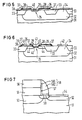
- An intermediate layer 12 made of SiO 2 is produced on a substrate 11 made of single-crystal silicon (see FIG. 1).
- the intermediate layer 12 is z. B. by thermal oxidation of the surface of the substrate 11 in a thickness of z. B. up to 30 nm or by deposition of SiO 2 from the gas phase after decomposition of Si (OC 2 H 5 ) 4 (so-called TEOS) in a thickness of z. B. 20 nm formed.
- a doped glass layer 13 is formed on the intermediate layer 12.
- the doped glass layer 13 is by CVD deposition of (B (0Si (CH 3 ) 3 ) 3 ) at a temperature of z. B. 800 to 850 ° C, preferably 840 ° C, formed.
- the doped glass layer 13 is z. B. generated in a thickness of 100 nm. It has a boron dopant concentration of approximately 4.3 ⁇ 10 22 cm -3 .
- the doped glass layer 13 is structured such that it covers the surface of the substrate 11 in the area in which a doped region 14 is to be formed.
- the doped region 14 is formed by diffusion of the dopant from the doped glass layer 13 through the intermediate layer 12 in the substrate 11. The depth of the doped region 14 depends on the thickness and density of the intermediate layer 12 (see FIG. 2).
- a structure 25 with a vertical flank 26 is produced on a substrate 21 made of single-crystal silicon (see FIG. 3).
- the structure 25 is formed from a polysilicon layer 251 and an SiO 2 layer 252 arranged thereon.
- an intermediate layer 22 is produced over the entire surface and in conformity.
- the intermediate layer 22 is z. B. by thermal oxidation or by CVD deposition of TEOS in a thickness of z. B. 20 nm formed.
- a doped glass layer 23 is deposited over the entire surface and conformally on the intermediate layer 22.
- the doped glass layer 23 is z. B. formed by CVD deposition of B (OSi (CH 3 ) 3 ) 3 .
- the doped glass layer 23 and the intermediate layer 22 are etched back, so that an etching residue, a so-called spacer 27, is formed on the flanks, while all flat areas are etched free.
- the spacer 27 is arranged on the flank 26 of the structure 25 (see FIG. 4).
- a doped region 24 is generated by diffusion of the dopant from the doped glass layer 23 through the intermediate layer 22 in the substrate 21.
- the position of the doped region 24 in relation to the flank 26 of the structure 25 is self-adjusted by the spacer technique.
- the method according to the invention is suitable for use in the manufacture of a bipolar transistor. It is also particularly suitable for producing an active base in a bipolar transistor in a double polysilicon process, as described, for. B. H. Kabza et al, IEEE-EDL (1989) Vol. 10, pp. 344-346.
- An n + -doped region 32 is arranged in a p-doped silicon substrate 31 for receiving the active parts of the bipolar transistor.
- Field oxide regions 33 isolate the n-doped region 32 on the surface of the substrate 31 in the substrate 31 against adjacent switching elements in the substrate 31. Furthermore, a field oxide region 33 insulates a deep collector connection 34 arranged in the n + -doped region 32 from the active transistor region 35.
- a base connection 36 is arranged on the surface of the substrate 31.
- the base connection 36 consists of B-doped polysilicon.
- the base connection 36 surrounds the active transistor region 35 in a ring shape.
- the base terminal 36 is on its surface with an insulation structure 37 made of z. B. SiO 2 provided.
- An intermediate layer 38 made of e.g. B. thermally generated silicon oxide in a thickness of up to 30 nm is arranged on the surface of the insulation structure 37 and the active transistor region 35.
- a doped glass layer 39 is arranged on the intermediate layer 38.
- the doped glass layer 39 is e.g. B. by CVD deposition of B (OSi (CH 3 ) 3 ) 3 at z. B. 840 ° C.
- the doped glass layer 39 has a thickness of e.g. B. 100 nm.
- An active base 40 is generated by diffusing out the dopant boron from the doped glass layer 39 through the intermediate layer 38 into the active transistor region 35 (see FIG. 5).
- the base width of the active base 40 ie the penetration depth of the dopant is z. B. 85 nm.
- an emitter connection 41 and a collector connection 42 are each formed from n-doped polysilicon (see Fig. 6).
- the emitter terminal 41 is formed above the active transistor region 35.
- the collector connection 42 is formed above the deep collector connection 34.
- the method according to the invention is also suitable for improving the contact between an active base and an inactive base in a bipolar transistor.
- 7 shows a section of a bipolar transistor.
- An active base 52 and an inactive base 53 are arranged in an n-doped region 51 of a silicon substrate.
- An emitter 54 is arranged on the surface of the substrate in the region of the active base 52.
- a base connection 55 made of B-doped polysilicon is arranged above the inactive base 53 on the surface of the substrate.
- the base terminal 55 is covered with an oxide layer 56.
- the oxide layer 56 and the base connection 55 have a common flank 57 which is perpendicular to the surface of the substrate.
- the spacer 58 has a layer 581 made of thermal oxide covering the flank 57 and the surface of the substrate and a portion 582 made of doped glass.
- the doped glass layer is produced by CVD deposition of B (OSi (CH 3 ) 3 ) 3 . In a temperature step at z. B.
- the dopant is diffused out of the part 582 of the spacer 58 through the layer 581 into the substrate 51. This creates a doped region 59 that connects the active base 52 with the inactive base 53. In this way, the base connection resistance is significantly improved.
- the doped region is arranged in a self-aligned manner by forming the spacer 58.
Landscapes
- Engineering & Computer Science (AREA)
- Microelectronics & Electronic Packaging (AREA)
- Power Engineering (AREA)
- Physics & Mathematics (AREA)
- Condensed Matter Physics & Semiconductors (AREA)
- General Physics & Mathematics (AREA)
- Computer Hardware Design (AREA)
- Ceramic Engineering (AREA)
- Manufacturing & Machinery (AREA)
- Bipolar Transistors (AREA)
Description
- Bei der Herstellung integrierter Schaltungen werden in Halbleitersubstraten, z. B. aus einkristallinem Silizium, Dotierstoffverteilungen erzeugt. Diese Dotierstoffverteilungen sind in den meisten Fällen örtlich begrenzt. Senkrecht zur Substratoberfläche weisen die Dotierstoffverteilungen dabei ein vorgegebenes Profil mit einem entsprechenden Gradienten auf.
- Dotierstoffe werden in Substrate durch Ionenimplantation oder Diffusion eingebracht. Bei der Ionenimplantation wird die Verteilung im Substrat durch eine Maske begrenzt, die mit Hilfe von Photolithographie hergestellt wird. Bei der Herstellung von Dotierstoffverteilungen mit Hilfe von Diffusion werden an der Oberfläche des Substrats z. B. dotierte Schichten angeordnet, aus denen der Dotierstoff ausdiffundiert. Die Form der Verteilung in der Ebene der Substratoberfläche wird dabei z. B. durch entsprechende Formgebung der dotierten Schicht bestimmt. Dazu wird die dotierte Schicht nach entsprechender photolithographischer Definition strukturiert.
- Aus EP-A-36 77 29 ist ein Verfahren zur Herstellung von BOX-Isolationsstrukturen bekannt. Dabei wird auf senkrechte Wände von in ein Substrat geätzten Gräben eine Barriereschicht aus thermischem SiO2 aufgewachsen. Darauf wird eine Borsilikatglasschicht als Diffusionsquelle mit einem Dotierstoffgehalt von weniger oder höchstens 1 Gewichtsprozent abgeschieden. Durch Ausdiffusion aus der Borsilikatglasschicht wird ein dotiertes Gebiet im Substrat hergestellt.
- Aus EP-A-33 93 85 ist bekannt, eine Borsilikatglasschicht durch Zersetzung von Tristrimethylsilylborat (B(OSi(CH3)3)3) herzustellen. Es wird darauf hingewiesen, daß eine auf diese Weise hergestellte Borsilikatglasschicht als Diffusionsquelle verwendet werden kann. Die erzielbare Borkonzentration im Substrat läßt sich dabei über den Borgehalt im Borsilikatglas, über die Temperatur, die Dauer und den Ambienten während des Eintreibschrittes steuern. Der Borgehalt solcher Borsilikat-glasschichten liegt zwischen 0,5 und 6 Gewichtsprozent.
- Das Dotierstoffprofil senkrecht zur Oberfläche des Substrats wird bei der Implantation im wesentlichen durch die Dosis und die Implantationsenergie bestimmt. Bei der Diffusion aus einer dotierten Schicht wird das Dotierstoffprofil senkrecht zur Substratoberfläche durch die in der dotierten Schicht enthaltene Dotierstoffmenge, die Segregation an der Grenzfläche zum Substrat und die Diffusionslänge bestimmt.
- Bei der Herstellung flacher Dotierstoffprofile d. h. von Profilen mit geringer Eindringtiefe der Dotierstoffe sind bei Verwendung der Ionenimplantation dadurch Grenzen gesetzt, daß die Reichweite aer Ionen in bestimmten Kristallrichtungen durch den Channeling-Effekt sehr groß ist. Ein weiteres praktisches Problem ist darin zu sehen, daß nur wenige Implantationsanlagen angeboten werden, mit denen eine Implantation mit weniger als 10 keV Implantationsenergie möglich ist. Solch geringe Energien sind jedoch erforderlich, um flache Dotierstoffprofile mit steilem Gradienten herzustellen.
- Bei der Herstellung von Bipolartransistoren mit sehr kurzen Schaltzeiten werden sehr geringe Eindringtiefen für Emitter/Basis- und Basis/Kollektor-Übergänge angestrebt. Im selbstjustierten Doppelpolysiliziumprozeß werden sowohl Basisanschlüsse als auch Emitteranschluß aus entsprechend dotiertem Polysilizium gebildet. Der Basisanschluß wird gegen den Emitteranschluß durch ein, nach einer unmaskierten, anisotropen Ätzung einer Oxidschicht zurückgebliebenes Ätzresiduum, den sogenannten SiO2-Spacer, isoliert (s. H. Kabza et al, IEEE-EDL (1989) Bd. 10, S. 344 - 346). Innerhalb der durch die Ätzresiduen definierten Fläche wird die aktive Basis hergestellt. Der Kontakt zwischen dem Basisanschluß und der aktiven Basis wird durch ein die aktive Basis ringförmig umgebendes, dotiertes Gebiet im Substrat unterhalb des Basisanschlusses gewährleistet. Dieses Gebiet wird inaktive Basis, auch externer Basisanschluß oder extrinsische Basis genannt. Die inaktive Basis muß die aktive Basis bei einer ausreichenden Dotierstoffkonzentration überlappen, um einen niederohmigen Basisanschluß-Widerstand zu liefern. Die inaktive Basis wird dabei durch Ausdiffusion aus dem Basisanschluß hergestellt.
- Wird die aktive Basis nach der Bildung der Ätzresiduen hergestellt, so kommt es zu einem zu hochohmigen Basisanschlußwiderstand, weil die aktive Basis und die inaktive Basis sich entweder nicht oder nur bei zu geringer Dotierstoffkonzentration überlappen (s. K. Ehinger et al, Proc. of ESSDERC, J. Phys., C4, S. 109 - 112 (1988)).
- Sehr steile Basis- und Emitterprofile mit geringer Eindringtiefe werden durch die sogenannte Doppeldiffusion erzielt. Unter Doppeldiffusion wird die sukzessive Diffusion von verschiedenen Dotierstoffen aus derselben polykristallinen Siliziumschicht verstanden. In diesem Fall wird die polykristalline Siliziumschicht für den Emitteranschluß zunächst mit Bor dotiert, dessen Ausdiffusion zur Bildung der aktiven Basis führt, und dann mit Arsen dotiert, dessen Ausdiffusion zur Ausbildung des Emitters führt. Der Überlapp von aktiver Basis und inaktiver Basis ist bei diesem Herstellverfahren ungenügend (s. K. Ehinger et al, Proc. of ESSDERC, J. Phys., C 4, S. 109 - 112 (1988)).
- Dieses Problem kann auf verschiedene Weisen gelöst werden: Die Basis kann vor der Bildung der Ätzresiduen durch Implantation hergestellt werden. Dadurch ist die Basis seitlich bis an den Rand des Basisanschlusses ausgedehnt. Damit ist zwar eine gute Überlappung zwischen aktiver und inaktiver Basis gegeben, es entstehen jedoch Implantationsschäden im aktiven Bereich des Transistors, die zu einer Reduzierung der Ausbeute führen können. Außerdem kann die Eindringtiefe der Dotierstoffe für die Basis wegen der Verwendung der Implantation nicht beliebig klein gemacht werden.
- Eine andere Möglichkeit besteht darin, vor der Bildung der Ätzresiduen einen Teil der Dotierstoffkonzentration für die aktive Basis mit geringer Energie zu implantieren. Anschließend wird durch Ausdiffusion aus der für den Emitteranschluß vorgesehenen, polykristallinen Siliziumschicht der Endwert der Basisdotierung eingestellt (s. T. Yamaguchi et al, IEEE - ED (1988) Bd. 35, S. 1247 - 1256). Dadurch wird jedoch die Dotierstoffkonzentration der aktiven Basis unter dem Emitterfenster vergrößert und das Basisprofil dabei verbreitert.
- Eine weitere Lösungsmöglichkeit besteht darin, das den Basisanschluß vom Emitteranschluß isolierende Ätzresiduum mit Bor zu dotieren (s. M. Nakamae, Proc. of ESSDERC (1987), S. 361 - 363). Durch Ausdiffusion aus dem Ätzresiduum wird die Dotierstoffkonzentration lokal an der Anschlußstelle inaktive Basis/aktive Basis erhöht. Die dabei erzielte Dotierstoffkonzentration ist vorgegeben durch die im Ätzresiduum deponierte Dotierstoffmenge, die Segregation an der Grenzfläche zum Substrat und die Diffusionslänge. Um den Basisanschlußwiderstand kontrolliert einstellen zu können, muß das Ätzresiduum daher aus einer SiO2-Verbindung gebildet werden, dessen Ausdiffusion bei vorgegebenem Temperaturbudget geeignet variierbar ist.
- Es hat sich herausgestellt, daß in beliebiger Konzentration dotierbare bordotierte SiO2-Verbindungen, wie sie in M. Nakamae, Proc. of ESSDERC (1987), S. 361 - 363 verwendet werden, sich in einem metastabilen Zustand befinden. Dadurch kommt es stellenweise zu Kristallisationen des Glases. An diesen Stellen ist dann die Charakteristik der Ausdiffusion verändert, so daß es zu großen ortsabhängigen Inhomogenitäten der Dotierstoffverteilung im Substrat kommt. Dieses wirkt sich negativ auf die gleichmäßige Einstellung eines niedrigen Basisanschlußwiderstands aus.
- Der Erfindung liegt das Problem zugrunde, ein Verfahren zur Herstellung eines dotierten Gebietes in einem Substrat anzugeben, mit dem die Dotierstoffverteilung auch bei einer geringen Eindringtiefe und einem steilen Gradienten des Dotierstoffes gut kontrollierbar ist und das bei der Herstellung eines Bipolartransistors zur lokalen Erhöhung der Dotierstoffkonzentration an der Anschlußstelle inaktive Basis/aktive Basis geeignet ist.
- Dieses Problem wird erfindungsgemäß gelöst in einem Verfahren nach Anspruch 1.
- Die Zwischenschicht begrenzt dabei die Ausdiffusion der Dotierstoffe in das Substrat. Durch Variation der Dicke und/oder der Dichte der Zwischenschicht wird die entstehende Dotierstoffverteilung in dem dotierten Gebiet festgelegt. Die Zwischenschicht wird z. B. aus SiO2, Si3N4, TiN usw. gebildet.
- Da sich die Dichte einer SiO2-Schicht mit den Herstellungs-bzw. Abscheidebedingungen ändert, kann bei Verwendung einer SiO2-Schicht durch entsprechende Wahl der Prozeßparameter Einfluß auf die entstehende Dotierstoffverteilung genommen werden. Beispielsweise zeigt thermisch erzeugtes SiO2 bei gleicher Dicke eine größere Diffusionsbarrierewirkung als SiO2, das durch Zersetzung von Si (OC2H5)4 (sogenanntes TEOS) in einem CVD-Abscheidereaktor erzeugt wurde.
- Als dotierte Glasschicht wird insbesondere eine Bor-dotierte Glasschicht verwendet, die durch CVD-Abscheidung von B(OSi(CH3)3)3 erzeugt wird. Eine so hergestellte dotierte Glasschicht zeigt keinerlei Kristallisation. Da in diesem Fall jedes abgeschiedene Molekül den Dotierstoff enthält, ist die Dotierstoffkonzentration des Bors in der so hergestellten dotierten Glasschicht konstant. Eine solche dotierte Glasschicht stellt bei ausreichender Dicke praktisch eine unendliche Borquelle dar, was auch durch Messungen belegt ist.
- Durch Verwendung der Zwischenschicht kann eine so hergestellte, dotierte Glasschicht als Diffusionsquelle für dotierte Gebiete mit unterschiedlicher Eindringtiefe des Dotierstoffs Bor verwendet werden. Dabei liegt es im Rahmen der Erfindung, thermisch erzeugte Oxide mit Dicken bis zu 30 nm oder CVD-erzeugte SiO2-Schichten mit Dicken zwischen 10 nm und 100 nm zu verwenden. Die Zwischenschicht wirkt als Diffusionsbarriere und reduziert dadurch die Oberflächenkonzentration des Bors und damit die Eindringtiefe des Bors in das Substrat. Durch Variation der lokalen Dicke der Zwischenschicht kann darüberhinaus die Eindringtiefe des Dotierstoffs lokal gezielt eingestellt werden.
- Die Formgebung des dotierten Gebietes in der Ebene parallel zur Oberfläche des Substrats erfolgt z. B. durch Strukturierung der dotierten Glasschicht unter Verwendung von Photolithographie vor der Ausdiffusion. Auf diese Weise wird das dotierte Gebiet auf die mit der verbleibenden dotierten Glasschicht bedeckte Oberfläche des Substrats begrenzt. Dabei liegt es im Rahmen der Erfindung, die dotierte Glasschicht und die Zwischenschicht nach dem Temperaturschritt zur Ausdiffusion des Dotierstoffes wieder zu entfernen. Diese Ausführungsform findet insbesondere Anwendung bei der Herstellung einer aktiven Basis eines Bipolartransistors nach dem erfindungsgemäßen Verfahren.
- In einer weiteren Ausführungsform der Erfindung wird vor der Erzeugung der Zwischenschicht an der Oberfläche des Substrats eine Struktur gebildet, die eine zur Oberfläche des Substrats senkrechte Flanke aufweist. Die Zwischenschicht wird ganzflächig und konform auf der mit der Struktur versehenen Oberfläche des Substrats erzeugt. Darauf wird wiederum ganzflächig und konform die dotierte Glasschicht erzeugt. In einem anisotropen Ätzprozeß werden die dotierte Glasschicht und die Zwischenschicht zurückgeätzt, so daß an der senkrechten Flanke ein Ätzresiduum (Spacer) entsteht. Das dotierte Gebiet im Substrat wird dann in einem Temperaturschritt durch Ausdiffusion aus dem Ätzresiduum gebildet. In dem Ätzresiduum ist aufgrund der Herstellvorschrift zwischen der Oberfläche des Substrats und dem Teil aus dotierten Glas weiterhin ein Teil der Zwischenschicht angeordnet, die die Ausdiffusion begrenzt.
- In dieser Ausführungsform wird das dotierte Gebiet selbstjustiert zur Flanke der Struktur hergestellt. Bei der Spacerbildung ist keinerlei photolithographischer Schritt erforderlich. Diese Ausführungsform der Erfindung ist besonders geeignet, um bei der Herstellung eines Bipolartransistors einen guten Überlapp zwischen dessen aktiver und inaktiver Basis sicherzustellen. Das Ätzresiduum wird in diesem Fall an einer dem Emitterfenster zugewandten Flanke eines Basisanschlusses aus polykristallinem Silizium gebildet. Da die inaktive Basis durch Ausdiffusion aus dem Basisanschluß gebildet wird und die aktive Basis innerhalb des mit dem Ätzresiduum versehenen Emitterfensters gebildet wird, stellt das aus dem Ätzresiduum erfindungsgemäß erzeugte dotierte Gebiet einen guten Kontakt zwischen aktiver Basis und inaktiver Basis her.
- Weitere Ausgestaltungen der Erfindung gehen aus den übrigen Ansprüchen hervor.
- Im folgenden wird die Erfindung anhand von Ausführungsbeispielen und der Figuren näher erläutert.
- Fig. 1 und Fig. 2
- zeigt die Herstellung eines dotierten Gebietes durch Ausdiffusion aus einer dotierten Glasschicht, die mit Hilfe eines photolithographischen Schrittes strukturiert wurde.
- Fig. 3 und Fig. 4
- zeigt die Herstellung eines dotierten Gebietes aus einem selbstjustiert gebildeten Ätzresiduum aus dotiertem Glas.
- Fig. 5 und Fig. 6
- zeigt die Herstellung eines Bipolartransistors, bei dem die aktive Basis durch Ausdiffusion aus einer dotierten Glasschicht erzeugt wird.
- Fig. 7
- zeigt die Herstellung einer Verbindung zwischen einer aktiven Basis und einer inaktiven Basis eines Bipolartransistors.
- Auf einem Substrat 11 aus einkristallinem Silizium wird eine Zwischenschicht 12 aus SiO2 erzeugt (s. Fig. 1). Die Zwischenschicht 12 wird z. B. durch thermische Oxidation der Oberfläche des Substrats 11 in einer Dicke von z. B. bis zu 30 nm oder durch Abscheidung von SiO2 aus der Gasphase nach Zersetzung von Si(OC2H5)4 (sogenanntes TEOS) in einer Dicke von z. B. 20 nm gebildet.
- Auf der Zwischenschicht 12 wird eine dotierte Glasschicht 13 gebildet. Die dotierte Glasschicht 13 wird durch CVD-Abscheidung von (B(0Si(CH3)3)3) bei einer Temperatur von z. B. 800 bis 850 °C, vorzugsweise 840 °C, gebildet. Die dotierte Glasschicht 13 wird z. B. in einer Dicke von 100 nm erzeugt. Sie weist eine Dotierstoffkonzentration des Bors von etwa 4,3 x 1022 cm-3 auf.
- Nach entsprechender Maskierung mit Hilfe von Photolithographie wird die dotierte Glasschicht 13 so strukturiert, daß sie die Oberfläche des Substrats 11 bedeckt in dem Bereich, in dem ein dotiertes Gebiet 14 gebildet werden soll. In einem Temperaturschritt bei z. B. 1050 °C wird das dotierte Gebiet 14 durch Ausdiffusion des Dotierstoffes aus der dotierten Glasschicht 13 durch die Zwischenschicht 12 hindurch im Substrat 11 gebildet. Die Tiefe des dotierten Gebietes 14 hängt dabei ab von der Dicke und Dichte der Zwischenschicht 12 (s. Fig. 2).
- Auf einem Substrat 21 aus einkristallinem Silizium wird eine Struktur 25 mit einer senkrechten Flanke 26 erzeugt (s. Fig. 3). Die Struktur 25 wird aus einer Polysiliziumschicht 251 und einer darauf angeordneten SiO2-Schicht 252 gebildet. Auf der mit der Struktur 25 versehenen Oberfläche des Substrats 21 wird ganzflächig und konform eine Zwischenschicht 22 erzeugt. Die Zwischenschicht 22 wird z. B. durch thermische Oxidation oder durch CVD-Abscheidung von TEOS in einer Dicke von z. B. 20 nm gebildet. Auf der Zwischenschicht 22 wird eine dotierte Glasschicht 23 ganzflächig und konform abgeschieden. Die dotierte Glasschicht 23 wird z. B. durch CVD-Abscheidung von B(OSi(CH3)3)3 gebildet.
- In einem anisotropen Ätzprozeß werden die dotierte Glasschicht 23 und die Zwischenschicht 22 rückgeätzt, so daß ein Ätzresiduum, ein sogenannter Spacer 27, an den Flanken entsteht, während alle ebenen Bereiche freigeätzt werden. Der Spacer 27 ist an der Flanke 26 der Struktur 25 angeordnet (s. Fig. 4). In einem Temperaturschritt bei z. B. 1050 °C, 20 sec. lang wird durch Ausdiffusion des Dotierstoffes aus der dotierten Glasschicht 23 durch die Zwischenschicht 22 in das Substrat 21 ein dotiertes Gebiet 24 erzeugt. Die Lage des dotierten Gebietes 24 zur Flanke 26 der Struktur 25 ist dabei selbstjustiert durch die Spacertechnik.
- Das erfindungsgemäße Verfahren ist zum Einsatz bei der Herstellung eines Bipolartransistors geeignet. Es ist insbesondere auch geeignet zur Herstellung einer aktiven Basis bei einem Bipolartransistor in einem Doppelpolysiliziumprozeß, wie er z. B. in H. Kabza et al, IEEE-EDL (1989) Bd. 10, S. 344 - 346 beschrieben ist. In einem p-dotierten Siliziumsubstrat 31 ist zur Aufnahme der aktiven Teile des Bipolartransistors ein n+-dotierter Bereich 32 angeordnet. Feldoxidbereiche 33 isolieren den n-dotierten Bereich 32 an der Oberfläche des Substrats 31 im Substrat 31 gegen benachbarte Schaltelemente im Substrat 31. Des weiteren isoliert ein Feldoxidbereich 33 einen im n+-dotierten Bereich 32 angeordneten tiefreichenden Kollektoranschluß 34 gegen den aktiven Transistorbereich 35. An der Oberfläche des Substrats 31 ist ein Basisanschluß 36 angeordnet. Der Basisanschluß 36 besteht aus B-dotiertem Polysilizium. Der Basisanschluß 36 umgibt den aktiven Transistorbereich 35 ringförmig. Der Basisanschluß 36 ist an seiner Oberfläche mit einer Isolationsstruktur 37 aus z. B. SiO2 versehen. Eine Zwischenschicht 38 aus z. B. thermisch erzeugtem Siliziumoxid in einer Dicke von bis zu 30 nm ist an der Oberfläche der Isolationsstruktur 37 und des aktiven Transistorbereichs 35 angeordnet. Auf der Zwischenschicht 38 ist eine dotierte Glasschicht 39 angeordnet. Die dotierte Glasschicht 39 ist z. B. durch CVD-Abscheidung von B(OSi(CH3)3)3 bei z. B. 840 °C erzeugt worden. Die dotierte Glasschicht 39 weist eine Dicke von z. B. 100 nm auf. Durch einen Temperaturschritt bei z. B. 1050 °C während z. B. 20 sec. wird durch Ausdiffusion des Dotierstoff Bor aus der dotierten Glasschicht 39 durch die Zwischenschicht 38 in den aktiven Transistorbereich 35 hinein eine aktive Basis 40 erzeugt (s. Fig. 5). Die Basisweite der aktiven Basis 40 (d. h. die Eindringtiefe des Dotierstoffes) beträgt z. B. 85 nm.
- Nach Entfernen der dotierten Glasschicht 39 und der Zwischenschicht 38, so daß an den Flanken Ätzresiduen aus Bor-dotiertem Glas und darunterliegendem Oxid stehen bleiben, während die ebenen Flächen freigeätzt sind, wird ein Emitteranschluß 41 und ein Kollektoranschluß 42 jeweils aus n-dotiertem Polysilizium gebildet (s. Fig. 6). Der Emitteranschluß 41 wird dabei oberhalb des aktiven Transistorbereichs 35 gebildet. Der Kollektoranschluß 42 wird oberhalb des tiefreichenden Kollektoranschluß 34 gebildet. Nach Ausdiffusion von Dotierstoff aus dem Emitteranschluß 41 zur Bildung eines Emitters 43 und nach Ausdiffusion von Dotierstoff aus dem Basisanschluß 36 zur Bildung einer inaktiven Basis 44, die die aktive Basis 40 ringförmig umgibt und anschließt, wird der Bipolartransistor durch Öffnen eines Kontaktloches 45 auf den Basisanschluß 36 fertiggestellt (s. Fig. 6).
- Das erfindungsgemäße Verfahren ist auch geeignet zur Verbesserung des Kontaktes zwischen einer aktiven Basis und einer inaktiven Basis in einem Bipolartransistor. In Fig. 7 ist ein Ausschnitt aus einem Bipolartransistor dargestellt. In einem n-dotierten Bereich 51 eines Siliziumsubstrates sind eine aktive Basis 52 und eine inaktive Basis 53 angeordnet. An der Oberfläche des Substrats ist im Bereich der aktiven Basis 52 ein Emitter 54 angeordnet. Oberhalb der inaktiven Basis 53 ist auf der Oberfläche des Substrats ein Basisanschluß 55 aus B-dotiertem Polysilizium angeordnet. Der Basisanschluß 55 ist mit einer Oxidschicht 56 bedeckt. Die Oxidschicht 56 und der Basisanschluß 55 weisen eine gemeinsame, zur Oberfläche des Substrats senkrechte Flanke 57 auf.
- Aus einer z. B. 10 nm dicken Zwischenschicht aus thermischen Oxid, die auf der Oberfläche der Oxidschicht 56, der Flanke 57 und des Substrats angeordnet ist, und aus einer darauf angeordneten dotierten Glasschicht wird ein Spacer 58 an der Flanke 57 gebildet. Dies erfolgt durch anisotropes Rückätzen, wie anhand von Fig. 3 und 4 ausführlich beschrieben. Der Spacer 58 weist eine die Flanke 57 und die Oberfläche des Substrats bedeckende Schicht 581 aus thermischem Oxid und einen Anteil 582 aus dotiertem Glas auf. Die dotierte Glasschicht wird durch CVD-Abscheidung von B(OSi(CH3)3)3 erzeugt. In einem Temperaturschritt bei z. B. 1050 °C wird der Dotierstoff aus dem Teil 582 des Spacers 58 durch die Schicht 581 in das Substrat 51 ausdiffundiert. Dadurch entsteht ein dotiertes Gebiet 59, das die aktive Basis 52 mit der inaktiven Basis 53 verbindet. Auf diese Weise wird der Basisanschlußwiderstand deutlich verbessert. Die Anordnung des dotierten Gebietes erfolgt selbstjustiert über die Bildung des Spacers 58.
Claims (9)
- Verfahren zur Herstellung eines dotierten Gebietes in einem Substrat mit folgenden Schritten:a) auf der Oberfläche des Substrats (21) aus Halbleitermaterial wird eine Struktur (25) gebildet, die eine senkrechte Flanke (26) aufweist,b) auf der mit der Struktur (25) versehenen Oberfläche des Substrats (21) wird eine Zwischenschicht (22) ganzflächig und konform erzeugt,c) auf der Zwischenschicht (22) wird ganzflächig und konform durch CVD-Abscheidung von (B(OSi)CH3)3)3) eine dotierte Glasschicht (23) erzeugt,d) in einem anisotropen Ätzprozeß werden die dotierte Glasschicht (23) und die Zwischenschicht (22) rückgeätzt, so daß an der senkrechten Flanke (26) ein Ätzresiduum (27) entsteht,e) in einem Temperaturschritt wird das dotierte Gebiet (24) in dem Substrat (21) durch Ausdiffusion aus dem Ätzresiduum (27) gebildet,f) die Zwischenschicht (22), durch die der Dotierstoff bei der Bildung des dotierten Gebietes (24) diffundiert, wird aus einem Material gebildet, das als Diffusionsbarriere für den Dotierstoff wirkt, so daß sie die Dotierstoffkonzentration im dotierten Gebiet (24) begrenzt.
- Verfahren nach Anspruch 1,
bei dem das Substrat (21) aus einkristallinem Silizium besteht. - Verfahren nach Anspruch 1 oder 2,
bei dem die CVD-Abscheidung bei 800 bis 850°C durchgeführt wird. - Verfahren nach einem der Ansprüche 1 bis 3,
bei dem die Zwischenschicht (22) durch thermische Oxidation in einer Dicke von bis zu 30 nm gebildet wird. - Verfahren nach einem der Ansprüche 1 bis 3,
bei dem die Zwischenschicht (22) durch CVD-Abscheidung von Si(OC2H5)4 (TEOS) in einer Dicke von 10 bis 100 nm gebildet wird. - Verfahren nach einem der Ansprüche 1 bis 5,
bei dem der Temperaturschritt zur Ausdiffusion bei 850°C bis 1000°C während 4 bis 20 min oder bei 900°C bis 1100°C während 1 bis 120 sec. erfolgt. - Verfahren nach einem der Ansprüche 1 bis 6,
bei dem die dotierte Glasschicht und die Zwischenschicht nach dem Temperaturschritt zur Ausdiffusion entfernt wird. - Verfahren nach einem der Ansprüche 1 bis 7,
bei dem die Struktur (25) an der Oberfläche des Substrats (21) dotiertes polykristallines Silizium (251) enthält. - Anwendung des Verfahren nach einem der Ansprüche 1 bis 8 bei der Herstellung eines Bipolartransistors.
Applications Claiming Priority (2)
| Application Number | Priority Date | Filing Date | Title |
|---|---|---|---|
| DE4120268 | 1991-06-19 | ||
| DE4120268 | 1991-06-19 |
Publications (2)
| Publication Number | Publication Date |
|---|---|
| EP0520214A1 EP0520214A1 (de) | 1992-12-30 |
| EP0520214B1 true EP0520214B1 (de) | 1996-09-18 |
Family
ID=6434308
Family Applications (1)
| Application Number | Title | Priority Date | Filing Date |
|---|---|---|---|
| EP92109303A Expired - Lifetime EP0520214B1 (de) | 1991-06-19 | 1992-06-02 | Verfahren zur Herstellung eines dotierten Gebietes in einem Substrat und Anwendung bei der Herstellung eines Bipolartransistors |
Country Status (5)
| Country | Link |
|---|---|
| US (1) | US5273934A (de) |
| EP (1) | EP0520214B1 (de) |
| JP (1) | JPH05190481A (de) |
| KR (1) | KR100285826B1 (de) |
| DE (1) | DE59207159D1 (de) |
Families Citing this family (7)
| Publication number | Priority date | Publication date | Assignee | Title |
|---|---|---|---|---|
| TW304293B (en) * | 1996-11-18 | 1997-05-01 | United Microelectronics Corp | Manufacturing method for shallow trench isolation |
| KR100245813B1 (ko) * | 1997-05-28 | 2000-03-02 | 윤종용 | 자기정합형 더블 폴리실리콘 바이폴라 트랜지스터및 그의 제조방법 |
| US5926715A (en) * | 1997-06-04 | 1999-07-20 | Mosel Vitelic Inc. | Method of forming lightly-doped drain by automatic PSG doping |
| US6498079B1 (en) * | 2000-07-27 | 2002-12-24 | Stmicroelectronics, Inc. | Method for selective source diffusion |
| US7649141B2 (en) * | 2003-06-30 | 2010-01-19 | Advent Solar, Inc. | Emitter wrap-through back contact solar cells on thin silicon wafers |
| US20050172996A1 (en) | 2004-02-05 | 2005-08-11 | Advent Solar, Inc. | Contact fabrication of emitter wrap-through back contact silicon solar cells |
| US20080150084A1 (en) * | 2006-12-01 | 2008-06-26 | Advent Solar, Inc. | Phosphorus-Stabilized Transition Metal Oxide Diffusion Barrier |
Family Cites Families (14)
| Publication number | Priority date | Publication date | Assignee | Title |
|---|---|---|---|---|
| US3764411A (en) * | 1970-06-23 | 1973-10-09 | Gen Electric | Glass melt through diffusions |
| US3728784A (en) * | 1971-04-15 | 1973-04-24 | Monsanto Co | Fabrication of semiconductor devices |
| US3775197A (en) * | 1972-01-05 | 1973-11-27 | A Sahagun | Method to produce high concentrations of dopant in silicon |
| US3798081A (en) * | 1972-02-14 | 1974-03-19 | Ibm | Method for diffusing as into silicon from a solid phase |
| JPS5694751A (en) * | 1979-12-28 | 1981-07-31 | Fujitsu Ltd | Vapor growth method |
| US4464212A (en) * | 1982-12-13 | 1984-08-07 | International Business Machines Corporation | Method for making high sheet resistivity resistors |
| FR2549293B1 (fr) * | 1983-07-13 | 1986-10-10 | Silicium Semiconducteur Ssc | Transistor bipolaire haute frequence et son procede de fabrication |
| US4604150A (en) * | 1985-01-25 | 1986-08-05 | At&T Bell Laboratories | Controlled boron doping of silicon |
| GB8527062D0 (en) * | 1985-11-02 | 1985-12-04 | Plessey Co Plc | Mos transistor manufacture |
| JPH0766968B2 (ja) * | 1987-08-24 | 1995-07-19 | 株式会社日立製作所 | 半導体装置及びその製造方法 |
| JPH01123417A (ja) * | 1987-11-07 | 1989-05-16 | Mitsubishi Electric Corp | 半導体装置の製造方法 |
| ATE112097T1 (de) * | 1988-04-26 | 1994-10-15 | Siemens Ag | Verfahren zum herstellen borhaltiger und/oder phosphorhaltiger silikatglasschichten für höchstintegrierte halbleiterschaltungen. |
| JPH0231425A (ja) * | 1988-07-21 | 1990-02-01 | Fujitsu Ltd | 半導体装置の製造方法 |
| IT1225625B (it) * | 1988-11-03 | 1990-11-22 | Sgs Thomson Microelectronics | Procedimento per la realizzazione di strutture di isolamento incassate nel substrato di silicio per dispositivi cmos ed nmos. |
-
1992
- 1992-05-11 US US07/881,166 patent/US5273934A/en not_active Expired - Fee Related
- 1992-06-02 EP EP92109303A patent/EP0520214B1/de not_active Expired - Lifetime
- 1992-06-02 DE DE59207159T patent/DE59207159D1/de not_active Expired - Fee Related
- 1992-06-17 JP JP4184548A patent/JPH05190481A/ja active Pending
- 1992-06-19 KR KR1019920010632A patent/KR100285826B1/ko not_active IP Right Cessation
Also Published As
| Publication number | Publication date |
|---|---|
| DE59207159D1 (de) | 1996-10-24 |
| EP0520214A1 (de) | 1992-12-30 |
| KR100285826B1 (ko) | 2001-04-16 |
| US5273934A (en) | 1993-12-28 |
| KR930001469A (ko) | 1993-01-16 |
| JPH05190481A (ja) | 1993-07-30 |
Similar Documents
| Publication | Publication Date | Title |
|---|---|---|
| EP0001550B1 (de) | Integrierte Halbleiteranordnung für eine Bauelementstruktur mit kleinen Abmessungen und zugehöriges Herstellungsvefahren | |
| EP0036634B1 (de) | Verfahren zur Herstellung einer bipolaren Transistorstruktur | |
| EP0010624B1 (de) | Verfahren zur Ausbildung sehr kleiner Maskenöffnungen für die Herstellung von Halbleiterschaltungsanordnungen | |
| DE2317577C2 (de) | Verfahren zur Herstellung dielektrisch isolierter Halbleiteranordnungen | |
| EP0931338B1 (de) | Verfahren zur herstellung eines mos-transistors | |
| EP0001574B1 (de) | Halbleiteranordnung für Widerstandsstrukturen in hochintegrierten Schaltkreisen und Verfahren zur Herstellung dieser Halbleiteranordnung | |
| EP0631306A1 (de) | Verfahren zur Herstellung von einem Isolationsgraben in einem Substrat für Smart-Power-Technologien | |
| DE3129558C2 (de) | ||
| DE19806838A1 (de) | Vertikaler Siliciumcarbid-MOSFET und Verfahren zur Herstellung desselben | |
| EP0920059A2 (de) | Speicherzellenanordnung und Verfahren zu deren Herstellung | |
| EP0010633A1 (de) | Verfahren zur Herstellung sehr schmaler Dosierungsgebiete in einem Halbleiterkörper sowie Verwendung dieses Verfahrens bei der Erzeugung von voneinander isolierten Halbleiterkörperbereichen, Bipolar-Halbleiteranordnungen, integrieten Injektionslogikschaltungen und doppelt diffundierten FET-Halbleiteranordnungen | |
| DE19526184A1 (de) | Verfahren zur Herstellung eines MOS-Transistors | |
| DE69230988T2 (de) | Verfahren zum Herstellen einer Anordnung, bei dem ein Stoff in einen Körper implantiert wird | |
| EP0006510A1 (de) | Verfahren zum Erzeugen aneinander grenzender, unterschiedlich dotierter Siliciumbereiche | |
| DE2510593C3 (de) | Integrierte Halbleiter-Schaltungsanordnung | |
| DE4409875C2 (de) | Verfahren zur Herstellung eines MOS Transistors unter Verwendung einer doppelt dotierten Schicht | |
| EP0520214B1 (de) | Verfahren zur Herstellung eines dotierten Gebietes in einem Substrat und Anwendung bei der Herstellung eines Bipolartransistors | |
| DE2942236C2 (de) | Verfahren zur Herstellung einer Halbleiteranordnung | |
| DE4211050A1 (de) | Verfahren zur Herstellung eines Bipolartransistors in einem Substrat | |
| EP0467081A2 (de) | Verfahren zur Herstellung eines Bipolartransistors | |
| DE69033593T2 (de) | Verfahren zur Herstellung einer integrierten Halbleiterschaltung mit einer Isolationszone | |
| WO2003015163A2 (de) | Verfahren zum parallelen herstellen eines mos-transistors und eines bipolartransistors | |
| EP0875931B1 (de) | Verfahren zur Herstellung einer CMOS-Schaltungsanordnung | |
| DE69431609T2 (de) | Verfahren zur Herstellung einer Halbleiteranordnung mit einem Bipolartransistor | |
| WO2001059845A2 (de) | Bipolartransistor |
Legal Events
| Date | Code | Title | Description |
|---|---|---|---|
| PUAI | Public reference made under article 153(3) epc to a published international application that has entered the european phase |
Free format text: ORIGINAL CODE: 0009012 |
|
| AK | Designated contracting states |
Kind code of ref document: A1 Designated state(s): DE FR GB IT |
|
| 17P | Request for examination filed |
Effective date: 19930122 |
|
| 17Q | First examination report despatched |
Effective date: 19941219 |
|
| GRAH | Despatch of communication of intention to grant a patent |
Free format text: ORIGINAL CODE: EPIDOS IGRA |
|
| GRAH | Despatch of communication of intention to grant a patent |
Free format text: ORIGINAL CODE: EPIDOS IGRA |
|
| GRAA | (expected) grant |
Free format text: ORIGINAL CODE: 0009210 |
|
| AK | Designated contracting states |
Kind code of ref document: B1 Designated state(s): DE FR GB IT |
|
| REF | Corresponds to: |
Ref document number: 59207159 Country of ref document: DE Date of ref document: 19961024 |
|
| ET | Fr: translation filed | ||
| ITF | It: translation for a ep patent filed | ||
| GBT | Gb: translation of ep patent filed (gb section 77(6)(a)/1977) |
Effective date: 19961122 |
|
| PLBE | No opposition filed within time limit |
Free format text: ORIGINAL CODE: 0009261 |
|
| STAA | Information on the status of an ep patent application or granted ep patent |
Free format text: STATUS: NO OPPOSITION FILED WITHIN TIME LIMIT |
|
| 26N | No opposition filed | ||
| PGFP | Annual fee paid to national office [announced via postgrant information from national office to epo] |
Ref country code: GB Payment date: 20010612 Year of fee payment: 10 |
|
| PGFP | Annual fee paid to national office [announced via postgrant information from national office to epo] |
Ref country code: FR Payment date: 20010622 Year of fee payment: 10 |
|
| PGFP | Annual fee paid to national office [announced via postgrant information from national office to epo] |
Ref country code: DE Payment date: 20010823 Year of fee payment: 10 |
|
| REG | Reference to a national code |
Ref country code: GB Ref legal event code: IF02 |
|
| PG25 | Lapsed in a contracting state [announced via postgrant information from national office to epo] |
Ref country code: GB Free format text: LAPSE BECAUSE OF NON-PAYMENT OF DUE FEES Effective date: 20020602 |
|
| PG25 | Lapsed in a contracting state [announced via postgrant information from national office to epo] |
Ref country code: DE Free format text: LAPSE BECAUSE OF NON-PAYMENT OF DUE FEES Effective date: 20030101 |
|
| GBPC | Gb: european patent ceased through non-payment of renewal fee |
Effective date: 20020602 |
|
| PG25 | Lapsed in a contracting state [announced via postgrant information from national office to epo] |
Ref country code: FR Free format text: LAPSE BECAUSE OF NON-PAYMENT OF DUE FEES Effective date: 20030228 |
|
| REG | Reference to a national code |
Ref country code: FR Ref legal event code: ST |
|
| PG25 | Lapsed in a contracting state [announced via postgrant information from national office to epo] |
Ref country code: IT Free format text: LAPSE BECAUSE OF NON-PAYMENT OF DUE FEES Effective date: 20050602 |