EP0516042A2 - Système de traitement d'erreur pour des cellules à ATM - Google Patents
Système de traitement d'erreur pour des cellules à ATM Download PDFInfo
- Publication number
- EP0516042A2 EP0516042A2 EP92108843A EP92108843A EP0516042A2 EP 0516042 A2 EP0516042 A2 EP 0516042A2 EP 92108843 A EP92108843 A EP 92108843A EP 92108843 A EP92108843 A EP 92108843A EP 0516042 A2 EP0516042 A2 EP 0516042A2
- Authority
- EP
- European Patent Office
- Prior art keywords
- error
- cell
- processing system
- atm
- decision signals
- Prior art date
- Legal status (The legal status is an assumption and is not a legal conclusion. Google has not performed a legal analysis and makes no representation as to the accuracy of the status listed.)
- Granted
Links
Images


Classifications
-
- H—ELECTRICITY
- H04—ELECTRIC COMMUNICATION TECHNIQUE
- H04Q—SELECTING
- H04Q11/00—Selecting arrangements for multiplex systems
- H04Q11/04—Selecting arrangements for multiplex systems for time-division multiplexing
- H04Q11/0428—Integrated services digital network, i.e. systems for transmission of different types of digitised signals, e.g. speech, data, telecentral, television signals
- H04Q11/0478—Provisions for broadband connections
-
- H—ELECTRICITY
- H04—ELECTRIC COMMUNICATION TECHNIQUE
- H04L—TRANSMISSION OF DIGITAL INFORMATION, e.g. TELEGRAPHIC COMMUNICATION
- H04L1/00—Arrangements for detecting or preventing errors in the information received
- H04L1/0078—Avoidance of errors by organising the transmitted data in a format specifically designed to deal with errors, e.g. location
- H04L1/0083—Formatting with frames or packets; Protocol or part of protocol for error control
-
- H—ELECTRICITY
- H04—ELECTRIC COMMUNICATION TECHNIQUE
- H04L—TRANSMISSION OF DIGITAL INFORMATION, e.g. TELEGRAPHIC COMMUNICATION
- H04L12/00—Data switching networks
- H04L12/54—Store-and-forward switching systems
- H04L12/56—Packet switching systems
- H04L12/5601—Transfer mode dependent, e.g. ATM
- H04L2012/5638—Services, e.g. multimedia, GOS, QOS
- H04L2012/5646—Cell characteristics, e.g. loss, delay, jitter, sequence integrity
Definitions
- the present invention generally relates to communications networks employing an ATM (Asynchronous Transfer Mode) transmission system. More particularly, the present invention is concerned with an ATM cell error processing system which detects an error in an ATM cell and processes such a defective ATM cell in a predetermined manner.
- ATM Asynchronous Transfer Mode
- Fig. 1-(a) shows an ATM layer data format
- Fig. 1-(b) shows an AAL (ATM Adaptation Layer) data format.
- AAL ATM Adaptation Layer
- Fig. 1-(b) shows a data format of the class-3 AAL, which is one of the four types of data formats, and which provides connection-oriented data communications services.
- the ATM cell consists of a header having five bytes (B), and an information field having 48 bytes.
- the ATM header includes a four-bit (b) undefined GFC (Generic Flow Control) field, an 8-bit VPI (Virtual Path Identifier) field, and a 16-bit VCI (Virtual Channel Identifier) field.
- the VPI and VCI are basic data used when an ATM switch determines a route.
- the ATM cell includes a 2-bit PT (Payload Type), a one-bit RS (Reserved) field, a one-bit CLP (Cell Loss Priority) field, and an 8-bit HEC (Header Error Control) field. Data in the CLP field shows whether or not the ATM cell should be discarded.
- the HEC is a CRC (Cyclic Redundancy Check) for the ATM header.
- the ATM header consists of 40 bits, which is equal to five bytes.
- the information field contains 44-byte information and other four-byte data, as shown in Fig. 1-(b).
- the four-byte data contained in the information field includes two-bit data showing a segment type (ST), four-bit data showing a sequence number (SN), 10 received bits (RES), six-bit length identifier (LI) data, and 10-bit CRC data.
- the segment type (ST) data is used for identifying the beginning and end of a message.
- the sequence number (SN) data shows the position of the cell in the message.
- the length identifier (LI) data shows the actual length of information.
- the 10-bit CRC data is an error correction code for the information field.
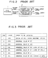
- Fig. 2 shows an overview of an ATM switching system, which comprises an ATM switch (or TC layer terminating equipment), and a message processing unit 2.
- the message processing unit 2 comprises a sender-side cell processor 2a, and a receiver-side cell processor 2b.
- the message processing unit 2 exchanges ATM cells with protocol data units (messages) in an upper layer.
- the sender-side cell processor 2a segments a message from the upper layer into units, each consisting of 44 bytes, and forms ATM cells conforming to the format shown in Fig. 1.
- the receiver-side cell processor 2b assembles ATM cells from the ATM switch 1 into a message conforming to the upper layer.
- the receiver-side cell processor 2b has a function of detecting an error in cell unit in order to determine whether or not each cell is correct.
- Fig. 3 shows the types of cell errors. In Fig. 3, three cell errors to be detected are defined for the ATM layer, and four cell errors to be detected are defined for the AAL.
- Fig. 4 is a diagram showing an overview of a conventional ATM cell error processing system. As shown in Fig. 4, the system includes a plurality of serially connected error processors 10 equal in number to the types of cell errors to be detected.
- the error processors 10 operate independently from each other, and each have the function of detecting a predetermined cell error, discarding an error cell and notifying a failure monitor unit 20 of detected error information.
- Fig. 5 shows the structure of each of the error processors 10 shown in Fig. 4.
- Each error processor 10 comprises an error check unit 21, a cell buffer 22 and an error cell discarding unit 23.
- the error check unit 21 receives an ATM cell and determines whether or not the ATM cell has a predetermined error. During this determination process, the ATM cell is queued in the cell buffer 22. If the error check unit 21 determines that the ATM cell has the predetermined error, it outputs a cell discarding instruction to the error cell discarding unit 23. In response to receipt of the cell discarding instruction, the error cell discarding unit 23 discards the ATM cell. The error check unit 21 then informs the failure monitor unit 20 of the result of the check.
- the cell buffer 22 must be provided in each error processor 10 in order to detect an error cell and discard it. Hence, a large quantity of hardware is needed to configure the system and a large amount of cell delay takes place.
- the cell error detecting processes are sequentially carried out by the error processors 10 in a predetermined order, because if a cell error has been detected during a series of error detecting processes, it is no longer necessary to execute the remaining cell error detecting processes. For example, the procedure for detecting cell errors is carried out in order of HEC, VCI, PT, CRC, ST, SN, MID and LI.
- the system shown in Fig. 4 is modified, as shown in Fig. 6.
- the failure monitor unit 20 outputs mask instructions to the error processors 10 that are to execute the error masking function.
- the system shown in Fig. 6 has the following disadvantages. That is, the control process of the failure monitor unit 20 is very complicated because it must individually output mask instructions to the error processors 10. Further, the ATM cells must be held in the cell buffers 22 even when these ATM cells are defective but not discarded.
- an error editing process based on the results of error check is very complicated or impossible because the error processors 10 separately generate the cell discarding instructions. For example, it is impossible to discard an ATM cell when it has a plurality of errors selected from among the predetermined cell error types.
- a more specific object of the present invention is to efficiently detect cell errors and efficiently execute an error editing process.
- an ATM cell error processing system comprising: a plurality of error detection means for respectively detecting predetermined cell errors and for respectively generating decision signals; error editing means, operatively coupled to the error detection means, for determining, on the basis of the decision signals, whether or not a cell related to the decision signals should be discarded; buffer means, coupled to at least one of the error detection means, for temporarily storing the cell; and error cell discarding means, coupled to the error editing means and the buffer means, for discarding the cell from the buffer means when the error editing means determines that the cell should be discarded and for relaying the cell when the error editing means does not determine that the cell should be discarded.
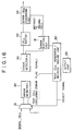
- Fig. 7 shows an ATM cell error processing system according to a first embodiment of the present invention.
- the system shown in Fig. 7 comprises error detectors 30 connected in series through a cell data line.
- the ATM cells and the check results are transferred through the error detectors 30.
- n error detectors 30 are connected in series.
- An error editing unit 31 which is connected to an output terminal of the error detector 30 of the final stage, receives error information therefrom, and executes an error process, such as a cell discarding process.
- a cell buffer 32 which is connected to the output terminal of the error detector 30 of the final stage, temporarily stores an ATM cell received therefrom.
- An error cell discarding unit 33 which is connected to an output terminal of the cell buffer 32, discards an error cell in response to receipt of a cell discarding instruction from the error editing unit 31.
- a failure monitor unit 20 communicates with the error editing unit 31.
- Each of the error detectors 30 checks whether or not the received cell has a predetermined cell error, and notifies the subsequent error detector 30 of the result of the check. It should be noted that each of the error detectors 30 does not have the function of discarding cells.
- the error editing unit 31 receives the results of the check obtained in the error detectors 30 via the error detector 30 of the final stage, and creates the cell discarding instruction on the basis of the received result of the check.
- each of the error detectors 30 does not have a cell buffer as shown in Fig.5. Hence, it becomes possible to reduce the hardware structure of the system. In addition, the results of the check obtained by the error detectors 30 are gathered in the error editing unit 31. Hence it becomes possible to conduct error editing efficiently.
- the first means has the function of placing the check result obtained in each of the error detectors 30 in a predetermined bit position of the next cell.
- the second means has the function of laying an error flag signal line carrying an error flag signal so that the error editing unit 31 is connected to the error detectors 30, and the results of check are placed in predetermined bit positions of the error flag signal.
- Fig. 8 shows the structure of each of the error detectors 30, which conform to the above-mentioned first means.
- Each of the error detectors 30 comprises a selector 40, an error check unit 41, and an error register 42.
- the selector 40 allows an input signal IN2 to pass in only a specific time slot, and allows an input signal IN1 to pass in other time slots.
- the above selecting operation of the selector 40 is controlled by a timing signal TIM generated by a timing controller 34.
- the timing signal TIM is maintained at, for example, a high level in only the specific time slot.
- the error check unit 41 receives the cell and determines whether or not the cell has a predetermined cell error.
- the error check unit 41 drops, from the received cell, data necessary for determining whether or not the cell received has the predetermined cell error. Data showing the result of the check is written into the error register 42, so that the content of the error register 42 is updated at each cell.
- the selector 40 selects the error register 42. In this manner, the result of the check obtained by the error detector shown in Fig. 8 is placed in a predetermined position in the cell data.
- Fig. 9 is a time chart showing the operation of one of the error detectors 30.
- the error detector 30 being considered determines whether or not the sequence number contained in the cell is correct and inserts the result of this check into the HEC field of the next cell.
- Fig. 9-(a) shows the beginnings of the cells
- Fig. 9-(b) shows cell data
- Fig. 9-(c) shows the results of checks cell
- Fig. 9-(d) shows the timing signal TIM.
- the result of the sequence number check on the cell #n-1 is written into the HEC field of the cell #n.
- the error check unit 41 executes the sequence number check on the cell #n during the time when the #n cell is passing through the error detector 30.
- the result of the sequence number check is written into the error register 42, and then written into the HEC field of the #n+1 cell subsequent to the cell #n while the cell #n+1 is passing through the error detector 30.
- Fig. 10 is a block diagram of the ATM cell error processing system of a second embodiment of the present invention designed to realize the aforementioned second means for informing the error editing unit 34 of the results of the checks obtained in the error detectors 30.
- An error signal flag line 50 is provided separately from the cell data line.
- Each of the error detectors 30 comprises error check units 43, and check result addition units 44.
- the error flag signal is synchronized with the cell data, and the bit position from the beginning of the cell shows the error content.
- the output terminal of the check result addition unit 44 of the final stage is connected to the input terminal of the error editing unit 34.
- the error check units 43 check the respective cells, and inform the corresponding check result addition units 44 of the results of the checks. For example, the check result addition units 44 are informed of data "0" when no errors have been detected, and data "1" when the predetermined errors have been respectively detected.
- Fig. 11 shows the structure of each of the check result addition units 44.
- Each unit 44 comprises an AND gate 44a, and an OR gate 44b.
- the AND gate 44a receives data showing the result of the check and a timing signal TIM for inserting the result of the check in the predetermined bit position.
- the timing signal TIM is generated by, for example, the timing generator 34 shown in Fig. 8.
- the OR gate 44b receives the error flag signal and an output signal of the AND gate 44a, and outputs the error flag signal together with the check result from the AND gate 44a inserted therein.
- the timing signal TIM indicates the bit position in the error flag signal into which the check result should be inserted. In this manner, the results of the checks are inserted into the respective bit positions in the error flag signal.
- the error editing unit 34 receives the error flag signal thus formed, and executes a predetermined editing process, such as a cell discarding process.
- Fig. 12 is a time chart showing the operation of one of the error detectors 30, which determines whether or not the sequence number is correct.
- Fig. 12-(a) shows the beginnings of the cells
- Fig. 12-(b) shows cell data
- Fig. 12-(c) shows the timing signal for inserting the result of check into the predetermined bit position
- Fig. 12-(d) shows the error flag signal.
- the error check unit 42 detects an error in the sequence number SN, the result of the check is inserted into the predetermined bit position in response to the timing signal TIM.
- Fig. 13 is a diagram showing error flags to be detected in the above-mentioned embodiment.
- cell data is illustrated so that it is processed in parallel form in groups of eight bits.
- Fig. 14 shows the structure of the error editing unit 34 in detail.
- parts which are the same as those shown in the previously described figures are given the same reference numerals.
- the following description of the error editing unit 34 will be given without distinguishing the aforementioned first and second means from each other.
- the error editing unit 31 comprises an error register 61, an error register 62, a decision making unit 63, and a controller 64, such as a processor.
- the error register 61 drops the error information from the cell data (first means) or the error flag signal (second means), and temporarily stores the error information.
- the error register 2 is updated when the error information concerning all error types to be detected for the cell being considered has been written in the error register 61.
- the decision making unit 63 makes a decision, on the basis of the error information stored in the error register 62, on whether or not the cell being considered should be discarded. For example, if at least one cell error has been detected, the cell is discarded.
- the decision making unit 63 outputs the cell discarding instruction to the error cell discarding unit 33.
- the error cell discarding unit 33 discards the error cell. In the above manner, each cell is temporarily stored (queued) in only the cell buffer 32. This facilitates error editing processing.
- Fig. 15 is a block diagram showing another structure of the error editing unit 31.
- the error editing unit 31 shown in Fig. 15 comprises an error register 65, and a logic circuit 70.
- the error register 65 has the functions of both the registers 61 and 62 shown in Fig. 14.
- the controller 64 shown in Fig. 14 is omitted in Fig. 15 for the sake of simplicity. Error information concerning all the error items is supplied to the failure monitor unit 20.
- the logic circuit 70 functions to define arbitrary combinations of necessary error data in the error information stored in the error register 65, and to discard mask information supplied from, for example, the failure monitor unit 20.
- the discard mask information may be supplied from the controller 64.
- the logic circuit 70 comprises a plurality of AND gates 71, and an OR gate 72.
- the AND gates 71 are supplied with the error information concerning the error items and the discard mask information. That is, each of the AND gates 71 receives one of the bits forming the error information and one of the bits forming the discard mask information, and outputs a resultant signal to the OR gate 72. When both bits are "1", the AND gate 71 outputs the cell discarding signal.
- the ATM cell error processing system of the present invention can be tested in the following manner.
- a test cell is used.
- the test cell is a special cell for use in testing, and a special header value, such as special VPI/VCI or special PT different from that of normal cells, and a test cell identification bit which shows the test cell and which is placed in a predetermined bit position in the error flag signal.
- Fig. 16 is a block diagram of a test system for testing the ATM cell error processing system of the present invention.
- the test system comprises a test cell generator/decision making unit 80, a selector 81, and an output unit 82.
- the unit 80 generates the above-mentioned test cell in which the special bit that shows the test cell is placed in the predetermined bit position.
- the test cell is supplied to the selector 81.
- the selector 81 selects a test cell in response to a select signal from the unit 80.
- the test cell passes through the selector 81, and is sequentially tested by the error detectors 30.
- the error editing unit 31 receives the error flag signal relating to the test cell from the error detector 30 of the final stage by detecting the test cell identification flag contained therein, and notifies the unit 80 of the identified error flag signal.
- the unit 80 checks the contents of the error flag signal, and determines whether or not each error detector 30 is operating normally. The results of this check are visually output through the output unit 82, which has a display and/or printer.
- the error editing unit 31 outputs the cell discarding instruction to the error cell discarding unit 33 in order to discard the test cell.
- the above test can be held in either a state where the inflow of normal cells is inhibited (off line) or a state where the test cell is inserted between normal cells (on line). It should be noted that the error detectors 30 can be tested in the same manner as in the case of the error editing processing. This means that the system does not require a special device for extracting the test cell, and a special device for discarding the test cell.
- Fig. 17 is a block diagram of an ATM cell error processing system according to a third embodiment of the present invention.
- the error detectors 30 are connected in parallel, as shown in Fig. 17.
- a cell normal cell or test cell
- passes through the selector 81 and is simultaneously applied to the cell buffer 32 and each of the error detectors 30.
- the error flag signal lines extending between the selector 81 and each of the error detectors 30, and between each of the error detectors 30 and the error editing unit 31 are omitted for the sake of convenience.
- the cell and the error flag signal are applied to each of the error detectors 30. When a cell error is detected, an error flag is set.
- one-bit error flag signals are output to the error editing unit 31 from the respective error detectors 30.
- the error editing unit 31 executes a predetermined error editing process on the basis of the error flag signals. It is also possible to use the error flag signal used in the previously described system. That is, the previously described error flag signal contains error flags of the respective error detectors 30.
Landscapes
- Engineering & Computer Science (AREA)
- Computer Networks & Wireless Communication (AREA)
- Signal Processing (AREA)
- Data Exchanges In Wide-Area Networks (AREA)
- Detection And Prevention Of Errors In Transmission (AREA)
Applications Claiming Priority (3)
| Application Number | Priority Date | Filing Date | Title |
|---|---|---|---|
| JP121070/91 | 1991-05-27 | ||
| JP3121070A JP3069389B2 (ja) | 1991-05-27 | 1991-05-27 | Atmセル誤り処理システム |
| JP12107091 | 1991-05-27 |
Publications (3)
| Publication Number | Publication Date |
|---|---|
| EP0516042A2 true EP0516042A2 (fr) | 1992-12-02 |
| EP0516042A3 EP0516042A3 (en) | 1997-03-12 |
| EP0516042B1 EP0516042B1 (fr) | 2000-07-19 |
Family
ID=14802098
Family Applications (1)
| Application Number | Title | Priority Date | Filing Date |
|---|---|---|---|
| EP92108843A Expired - Lifetime EP0516042B1 (fr) | 1991-05-27 | 1992-05-26 | Système de traitement d'erreur pour des cellules à ATM |
Country Status (6)
| Country | Link |
|---|---|
| US (1) | US5513191A (fr) |
| EP (1) | EP0516042B1 (fr) |
| JP (1) | JP3069389B2 (fr) |
| AU (1) | AU631081B1 (fr) |
| CA (1) | CA2069346C (fr) |
| DE (1) | DE69231264T2 (fr) |
Cited By (12)
| Publication number | Priority date | Publication date | Assignee | Title |
|---|---|---|---|---|
| WO1994013082A1 (fr) * | 1992-11-24 | 1994-06-09 | Telefonaktiebolaget Lm Ericsson | Systeme de surveillance des erreurs sur des bits, destine a une installation de commutation |
| EP0606729A2 (fr) * | 1993-01-11 | 1994-07-20 | AT&T Corp. | Format interne étendu de cellules à ATM |
| EP0607673A2 (fr) * | 1993-01-11 | 1994-07-27 | AT&T Corp. | Commutateur à ATM |
| EP0607672A2 (fr) * | 1993-01-11 | 1994-07-27 | AT&T Corp. | Dispositif de synchronisation de charge utile à ATM |
| EP0642228A2 (fr) * | 1993-07-05 | 1995-03-08 | Mitsubishi Denki Kabushiki Kaisha | Dispositif de transmission et de réception de données entrelacées codées pour la correction d'erreurs dans une trame de transmission |
| US5528763A (en) * | 1993-09-14 | 1996-06-18 | International Business Machines Corporation | System for admitting cells of packets from communication network into buffer of attachment of communication adapter |
| GB2313748A (en) * | 1996-05-31 | 1997-12-03 | Northern Telecom Ltd | Error detection/correction for ATM cells/frames |
| EP0863687A2 (fr) * | 1997-03-03 | 1998-09-09 | Toshiba Corporation | Commutateur ATM et méthode de traitement d'erreurs utilisée là-dedans |
| EP1093264A2 (fr) * | 1999-10-14 | 2001-04-18 | Alcatel Networks Corporation Societe Par Actions De Regime Federal De Reseaux Alcatel | Méthode et appareil pour vérification l' intégrité de données utiles et détection de modules défectueux dans des dispositifs de télécommunication |
| US6560653B1 (en) | 1997-08-08 | 2003-05-06 | Telefonaktiebolaget Lm Ericsson (Publ) | System and method for processing a signalling message in an ATM network |
| US6728921B1 (en) | 1996-05-31 | 2004-04-27 | Nortel Networks Limited | Cell based data transmission method |
| EP3087403A4 (fr) * | 2013-12-26 | 2017-10-18 | Intel Corporation | Améliorations d'un dispositif de resynchronisation d'interconnexion |
Families Citing this family (24)
| Publication number | Priority date | Publication date | Assignee | Title |
|---|---|---|---|---|
| JP2671821B2 (ja) * | 1994-09-28 | 1997-11-05 | 日本電気株式会社 | データ伝送装置 |
| JPH08186571A (ja) * | 1994-12-28 | 1996-07-16 | Fujitsu Ltd | Atmセル損失検出制御方式 |
| CA2152567C (fr) * | 1995-06-23 | 2000-01-11 | Kenneth M. Buckland | Methode pour effectuer directement le reassemblage de la couche d'adaptation 5 lors de transmissions en mode de transfert asynchrone (mta) |
| US5790567A (en) * | 1995-08-28 | 1998-08-04 | California Institute Of Technology | Parallel processing spacecraft communication system |
| KR0150522B1 (ko) * | 1995-12-19 | 1998-11-02 | 양승택 | 광대역 종합정보 통신망(b-isdn) 프로토콜 및 트래픽 시험 장치 및 그 방법 |
| US6028844A (en) * | 1996-01-25 | 2000-02-22 | Cypress Semiconductor Corp. | ATM receiver |
| JP2814993B2 (ja) * | 1996-06-28 | 1998-10-27 | 日本電気株式会社 | Atmセル導通試験方式 |
| DE19641399A1 (de) * | 1996-09-27 | 1998-04-02 | Siemens Ag | Verfahren zum Ermitteln von auf einer ATM-Übertragungsstrecke in ATM-Nutzzellen aufgetretenen Bitfehlern mit Hilfe von Monitoring-OAM-Zellen |
| KR100199959B1 (ko) * | 1996-10-14 | 1999-06-15 | 김영환 | 시디엠에이 이동통신 시스템의 패리티 검사장치 및 그 방법 |
| JP2836606B2 (ja) * | 1996-10-25 | 1998-12-14 | 日本電気株式会社 | Atmセル転送装置 |
| JPH10271112A (ja) * | 1997-03-21 | 1998-10-09 | Fujitsu Ltd | 非同期転送モード交換システムにおける課金情報救済システム |
| US6138253A (en) * | 1997-05-29 | 2000-10-24 | Oracle Corporation | Method and apparatus for reporting errors in a computer system |
| DE19738362B4 (de) * | 1997-09-02 | 2006-11-02 | Siemens Ag | Schaltungsanordnung und Verfahren zur Minimierung von Bitfehlern |
| KR100251735B1 (ko) * | 1997-12-29 | 2000-04-15 | 윤종용 | 에이티엠 스위치에서 저장영역 손실방지 장치 및방법 |
| US5923681A (en) * | 1998-02-24 | 1999-07-13 | Tektronix, Inc. | Parallel synchronous header correction machine for ATM |
| KR100434463B1 (ko) * | 1999-01-07 | 2004-06-05 | 삼성전자주식회사 | 부호분할다중접속 통신시스템의 데이터 통신 장치 및 방법 |
| JP2001053753A (ja) * | 1999-08-09 | 2001-02-23 | Fujitsu Ltd | Atmネットワークにおける現用/予備回線の切替え方法及びこれを使用するatm交換機 |
| US6639899B1 (en) * | 1999-10-14 | 2003-10-28 | Alcatel Canada Inc. | Method and apparatus for providing integral cell payload integrity verification in ATM Telecommunication devices |
| US8717868B2 (en) * | 2003-12-19 | 2014-05-06 | Rockstar Consortium Us Lp | Selective processing of damaged packets |
| KR100833600B1 (ko) * | 2006-08-25 | 2008-05-30 | 삼성전자주식회사 | 에러 정정 회로, 그 방법 및 상기 회로를 구비하는 반도체메모리 장치 |
| DE102007035262B4 (de) * | 2007-07-27 | 2018-05-24 | Texas Instruments Deutschland Gmbh | Empfänger und Verfahren zur Bearbeitung eines Datenpaketstroms bei Auftreten eines Fehlers auf der Bitübertragungsschicht |
| US8351426B2 (en) * | 2008-03-20 | 2013-01-08 | International Business Machines Corporation | Ethernet virtualization using assisted frame correction |
| JP5750387B2 (ja) * | 2012-03-07 | 2015-07-22 | 株式会社日立製作所 | フレーム制御装置、伝送装置、ネットワークシステム、バッファの読み出し制御方法 |
| JP6237074B2 (ja) * | 2013-10-02 | 2017-11-29 | 日本電気株式会社 | 通信装置および障害検出方法 |
Citations (2)
| Publication number | Priority date | Publication date | Assignee | Title |
|---|---|---|---|---|
| DE3841370A1 (de) * | 1987-12-08 | 1989-06-22 | Hitachi Ltd | Verfahren und vorrichtung fuer eine crc-berechnung |
| US4975906A (en) * | 1988-02-15 | 1990-12-04 | Hitachi, Ltd. | Network system |
Family Cites Families (3)
| Publication number | Priority date | Publication date | Assignee | Title |
|---|---|---|---|---|
| JP2677418B2 (ja) * | 1989-06-22 | 1997-11-17 | 富士通株式会社 | Atmスイッチの系切換方式 |
| CA2045460C (fr) * | 1989-11-29 | 1996-06-11 | Yumiko Kato | Systeme de commutation pour systeme duplex a mode de transfert asynchrone |
| EP0441168B1 (fr) * | 1990-02-06 | 1996-10-16 | ALCATEL ITALIA Società per Azioni | Système, structure de paquet et dispositif pour le traitement d'information de sortie d'un codeur de signal |
-
1991
- 1991-05-27 JP JP3121070A patent/JP3069389B2/ja not_active Expired - Fee Related
-
1992
- 1992-05-25 CA CA002069346A patent/CA2069346C/fr not_active Expired - Fee Related
- 1992-05-25 AU AU17145/92A patent/AU631081B1/en not_active Ceased
- 1992-05-26 EP EP92108843A patent/EP0516042B1/fr not_active Expired - Lifetime
- 1992-05-26 DE DE69231264T patent/DE69231264T2/de not_active Expired - Fee Related
- 1992-05-27 US US07/888,787 patent/US5513191A/en not_active Expired - Fee Related
Patent Citations (2)
| Publication number | Priority date | Publication date | Assignee | Title |
|---|---|---|---|---|
| DE3841370A1 (de) * | 1987-12-08 | 1989-06-22 | Hitachi Ltd | Verfahren und vorrichtung fuer eine crc-berechnung |
| US4975906A (en) * | 1988-02-15 | 1990-12-04 | Hitachi, Ltd. | Network system |
Non-Patent Citations (1)
| Title |
|---|
| A.T.R., vol. 23, no. 2, 1989, XP000609375 L. ZHANG, M.J. MILLER, K. SARKIES: "A Forward Error Protection Scheme for B-ISDN Using a Virtual Path (VP) Technique" * |
Cited By (29)
| Publication number | Priority date | Publication date | Assignee | Title |
|---|---|---|---|---|
| WO1994013082A1 (fr) * | 1992-11-24 | 1994-06-09 | Telefonaktiebolaget Lm Ericsson | Systeme de surveillance des erreurs sur des bits, destine a une installation de commutation |
| CN1051891C (zh) * | 1992-11-24 | 2000-04-26 | 艾利森电话股份有限公司 | 交换设备中的位错监测装置 |
| AU674370B2 (en) * | 1992-11-24 | 1996-12-19 | Telefonaktiebolaget Lm Ericsson (Publ) | An arrangement for bit error monitoring in switching equipment |
| EP0606729A3 (en) * | 1993-01-11 | 1996-12-18 | At & T Corp | Asynchronous transfer mode (atm) expanded internal cell format. |
| EP0606729A2 (fr) * | 1993-01-11 | 1994-07-20 | AT&T Corp. | Format interne étendu de cellules à ATM |
| EP0607673A2 (fr) * | 1993-01-11 | 1994-07-27 | AT&T Corp. | Commutateur à ATM |
| EP0607672A2 (fr) * | 1993-01-11 | 1994-07-27 | AT&T Corp. | Dispositif de synchronisation de charge utile à ATM |
| EP0607672A3 (en) * | 1993-01-11 | 1996-12-11 | At & T Corp | Asynchronous transfer mode (atm) payload synchronizer. |
| EP0607673A3 (en) * | 1993-01-11 | 1996-12-11 | At & T Corp | Asynchronous transfer mode (atm) switch fabric. |
| EP1333585A2 (fr) * | 1993-07-05 | 2003-08-06 | Mitsubishi Denki Kabushiki Kaisha | Emetteur de données entrelacées codées pour la correction d'erreurs dans une trame de transmission |
| EP0642228A2 (fr) * | 1993-07-05 | 1995-03-08 | Mitsubishi Denki Kabushiki Kaisha | Dispositif de transmission et de réception de données entrelacées codées pour la correction d'erreurs dans une trame de transmission |
| US5642365A (en) * | 1993-07-05 | 1997-06-24 | Mitsubishi Denki Kabushiki Kaisha | Transmitter for encoding error correction codes and a receiver for decoding error correction codes on a transmission frame |
| EP0642228A3 (fr) * | 1993-07-05 | 1996-11-27 | Mitsubishi Electric Corp | Dispositif de transmission et de réception de données entrelacées codées pour la correction d'erreurs dans une trame de transmission. |
| EP1056211A1 (fr) * | 1993-07-05 | 2000-11-29 | Mitsubishi Denki Kabushiki Kaisha | Emetteur et récepteur de données entrelacées codées pour la correction d'erreurs dans une trame de transmission avec détection de pertes de cellule |
| EP1333585A3 (fr) * | 1993-07-05 | 2003-08-13 | Mitsubishi Denki Kabushiki Kaisha | Emetteur de données entrelacées codées pour la correction d'erreurs dans une trame de transmission |
| US5528763A (en) * | 1993-09-14 | 1996-06-18 | International Business Machines Corporation | System for admitting cells of packets from communication network into buffer of attachment of communication adapter |
| GB2313748A (en) * | 1996-05-31 | 1997-12-03 | Northern Telecom Ltd | Error detection/correction for ATM cells/frames |
| US6728921B1 (en) | 1996-05-31 | 2004-04-27 | Nortel Networks Limited | Cell based data transmission method |
| GB2313748B (en) * | 1996-05-31 | 2000-12-20 | Northern Telecom Ltd | Cell based data transmission method |
| US6230297B1 (en) | 1996-05-31 | 2001-05-08 | Nortel Networks Limited | Cell based data transmission method |
| EP0863687A3 (fr) * | 1997-03-03 | 2000-01-05 | Kabushiki Kaisha Toshiba | Commutateur ATM et méthode de traitement d'erreurs utilisée là-dedans |
| EP0863687A2 (fr) * | 1997-03-03 | 1998-09-09 | Toshiba Corporation | Commutateur ATM et méthode de traitement d'erreurs utilisée là-dedans |
| US6560653B1 (en) | 1997-08-08 | 2003-05-06 | Telefonaktiebolaget Lm Ericsson (Publ) | System and method for processing a signalling message in an ATM network |
| EP1093264A2 (fr) * | 1999-10-14 | 2001-04-18 | Alcatel Networks Corporation Societe Par Actions De Regime Federal De Reseaux Alcatel | Méthode et appareil pour vérification l' intégrité de données utiles et détection de modules défectueux dans des dispositifs de télécommunication |
| EP1093264A3 (fr) * | 1999-10-14 | 2005-03-16 | Alcatel Canada Inc. | Méthode et appareil pour vérification l' intégrité de données utiles et détection de modules défectueux dans des dispositifs de télécommunication |
| US7420926B2 (en) | 1999-10-14 | 2008-09-02 | Alcatel-Lucent Canada Inc. | Method and apparatus for providing integral cell payload integrity verification and detecting defective modules in telecommunication devices |
| EP3087403A4 (fr) * | 2013-12-26 | 2017-10-18 | Intel Corporation | Améliorations d'un dispositif de resynchronisation d'interconnexion |
| US10534034B2 (en) | 2013-12-26 | 2020-01-14 | Intel Corporation | Interconnect retimer enhancements |
| US11675003B2 (en) | 2013-12-26 | 2023-06-13 | Intel Corporation | Interconnect retimer enhancements |
Also Published As
| Publication number | Publication date |
|---|---|
| EP0516042A3 (en) | 1997-03-12 |
| DE69231264D1 (de) | 2000-08-24 |
| CA2069346C (fr) | 1999-01-26 |
| AU631081B1 (en) | 1992-11-12 |
| CA2069346A1 (fr) | 1992-11-28 |
| JPH05136804A (ja) | 1993-06-01 |
| US5513191A (en) | 1996-04-30 |
| EP0516042B1 (fr) | 2000-07-19 |
| JP3069389B2 (ja) | 2000-07-24 |
| DE69231264T2 (de) | 2000-12-28 |
Similar Documents
| Publication | Publication Date | Title |
|---|---|---|
| US5513191A (en) | Asynchronous transfer mode (ATM) cell error processing system | |
| US6483854B1 (en) | Method and apparatus for using ATM queues for segmentation and reassembly of data frames | |
| EP0683948B1 (fr) | Procede de traitement de plans de commutation de redondance dans des commutateurs de paquets et commutateur de paquets permettant d'appliquer ce procede | |
| US5325358A (en) | Method and circuit arrangement for transmitting message packets via packet switching equipment, the message packets being transmitted on output trunks | |
| US5848067A (en) | AAL1 processing method and apparatus for parallelly executing sequence number processing and pointer comparison processing in ATM cell disassembly apparatus | |
| EP0600683A2 (fr) | Interface pour un réseau de paguets | |
| US5199028A (en) | Asynchronous time division network | |
| US6424632B1 (en) | Method and apparatus for testing packet data integrity using data check field | |
| US5729530A (en) | ATM switch | |
| EP0683949B1 (fr) | Procede de traitement de plans de commutation de redondance dans des commutateurs de paquets et commutateur permettant d'appliquer ce procede | |
| JPH0575639A (ja) | Atmスイツチのパス試験方式 | |
| US5153920A (en) | Method and circuit arrangement for the acceptance and forwarding of message cells transmitted according to an asynchronous transfer mode by an asynchronous transfer mode switching equipment | |
| EP0772371B1 (fr) | Vérification d'une unité de transport de réseau dans un environnement de réseaux | |
| EP0537382A1 (fr) | Arrangement et procédé pour contrôler de transfert des paquets | |
| US5946312A (en) | ATM cell transfer system in which use efficiency of transmission line is improved | |
| US6175567B1 (en) | Method and system for multiplexing/demultiplexing asynchronous transfer mode interprocessor communication (ATM IPC) cell in exchange | |
| EP1040625B1 (fr) | Commutateur a mode de transfert asynchrone | |
| US6411622B1 (en) | Method and apparatus for detecting timeout of ATM reception packet | |
| JP3152285B2 (ja) | Atmセル多重化方式 | |
| US5642347A (en) | Approach to direct performing asynchronous transfer mode (ATM) adaptation layer 5 reassembly | |
| JP2824483B2 (ja) | Atm交換機におけるスイッチ診断方式 | |
| JPH1065713A (ja) | Atmシステム用セル検出方法 | |
| KR20030009687A (ko) | 지에프피 수신 프레임의 경계식별 장치 및 그 방법 | |
| JP2948046B2 (ja) | Atm伝送システムにおけるデータチェック方式 | |
| JPH098816A (ja) | 非同期転送モード通信システムおよびそのセル分解装置ならびに非同期転送モード通信方式 |
Legal Events
| Date | Code | Title | Description |
|---|---|---|---|
| PUAI | Public reference made under article 153(3) epc to a published international application that has entered the european phase |
Free format text: ORIGINAL CODE: 0009012 |
|
| AK | Designated contracting states |
Kind code of ref document: A2 Designated state(s): DE FR GB |
|
| PUAL | Search report despatched |
Free format text: ORIGINAL CODE: 0009013 |
|
| AK | Designated contracting states |
Kind code of ref document: A3 Designated state(s): DE FR GB |
|
| 17P | Request for examination filed |
Effective date: 19970404 |
|
| 17Q | First examination report despatched |
Effective date: 19980313 |
|
| GRAG | Despatch of communication of intention to grant |
Free format text: ORIGINAL CODE: EPIDOS AGRA |
|
| GRAG | Despatch of communication of intention to grant |
Free format text: ORIGINAL CODE: EPIDOS AGRA |
|
| GRAH | Despatch of communication of intention to grant a patent |
Free format text: ORIGINAL CODE: EPIDOS IGRA |
|
| GRAH | Despatch of communication of intention to grant a patent |
Free format text: ORIGINAL CODE: EPIDOS IGRA |
|
| GRAA | (expected) grant |
Free format text: ORIGINAL CODE: 0009210 |
|
| AK | Designated contracting states |
Kind code of ref document: B1 Designated state(s): DE FR GB |
|
| REF | Corresponds to: |
Ref document number: 69231264 Country of ref document: DE Date of ref document: 20000824 |
|
| ET | Fr: translation filed | ||
| PLBE | No opposition filed within time limit |
Free format text: ORIGINAL CODE: 0009261 |
|
| STAA | Information on the status of an ep patent application or granted ep patent |
Free format text: STATUS: NO OPPOSITION FILED WITHIN TIME LIMIT |
|
| 26N | No opposition filed | ||
| REG | Reference to a national code |
Ref country code: GB Ref legal event code: IF02 |
|
| PGFP | Annual fee paid to national office [announced via postgrant information from national office to epo] |
Ref country code: FR Payment date: 20020508 Year of fee payment: 11 |
|
| PGFP | Annual fee paid to national office [announced via postgrant information from national office to epo] |
Ref country code: GB Payment date: 20020522 Year of fee payment: 11 |
|
| PGFP | Annual fee paid to national office [announced via postgrant information from national office to epo] |
Ref country code: DE Payment date: 20020529 Year of fee payment: 11 |
|
| PG25 | Lapsed in a contracting state [announced via postgrant information from national office to epo] |
Ref country code: GB Free format text: LAPSE BECAUSE OF NON-PAYMENT OF DUE FEES Effective date: 20030526 |
|
| PG25 | Lapsed in a contracting state [announced via postgrant information from national office to epo] |
Ref country code: DE Free format text: LAPSE BECAUSE OF NON-PAYMENT OF DUE FEES Effective date: 20031202 |
|
| GBPC | Gb: european patent ceased through non-payment of renewal fee |
Effective date: 20030526 |
|
| PG25 | Lapsed in a contracting state [announced via postgrant information from national office to epo] |
Ref country code: FR Free format text: LAPSE BECAUSE OF NON-PAYMENT OF DUE FEES Effective date: 20040130 |
|
| REG | Reference to a national code |
Ref country code: FR Ref legal event code: ST |