EP0515074A2 - Oscillateur contrôlé en fréquence pour une boucle à verrouillage de phase haute fréquence - Google Patents
Oscillateur contrôlé en fréquence pour une boucle à verrouillage de phase haute fréquence Download PDFInfo
- Publication number
- EP0515074A2 EP0515074A2 EP92304276A EP92304276A EP0515074A2 EP 0515074 A2 EP0515074 A2 EP 0515074A2 EP 92304276 A EP92304276 A EP 92304276A EP 92304276 A EP92304276 A EP 92304276A EP 0515074 A2 EP0515074 A2 EP 0515074A2
- Authority
- EP
- European Patent Office
- Prior art keywords
- frequency
- clock signal
- phase
- signal
- output
- Prior art date
- Legal status (The legal status is an assumption and is not a legal conclusion. Google has not performed a legal analysis and makes no representation as to the accuracy of the status listed.)
- Granted
Links
Images


Classifications
-
- H—ELECTRICITY
- H03—ELECTRONIC CIRCUITRY
- H03L—AUTOMATIC CONTROL, STARTING, SYNCHRONISATION, OR STABILISATION OF GENERATORS OF ELECTRONIC OSCILLATIONS OR PULSES
- H03L7/00—Automatic control of frequency or phase; Synchronisation
-
- H—ELECTRICITY
- H03—ELECTRONIC CIRCUITRY
- H03L—AUTOMATIC CONTROL, STARTING, SYNCHRONISATION, OR STABILISATION OF GENERATORS OF ELECTRONIC OSCILLATIONS OR PULSES
- H03L7/00—Automatic control of frequency or phase; Synchronisation
- H03L7/06—Automatic control of frequency or phase; Synchronisation using a reference signal applied to a frequency- or phase-locked loop
- H03L7/16—Indirect frequency synthesis, i.e. generating a desired one of a number of predetermined frequencies using a frequency- or phase-locked loop
-
- H—ELECTRICITY
- H03—ELECTRONIC CIRCUITRY
- H03B—GENERATION OF OSCILLATIONS, DIRECTLY OR BY FREQUENCY-CHANGING, BY CIRCUITS EMPLOYING ACTIVE ELEMENTS WHICH OPERATE IN A NON-SWITCHING MANNER; GENERATION OF NOISE BY SUCH CIRCUITS
- H03B21/00—Generation of oscillations by combining unmodulated signals of different frequencies
-
- H—ELECTRICITY
- H03—ELECTRONIC CIRCUITRY
- H03L—AUTOMATIC CONTROL, STARTING, SYNCHRONISATION, OR STABILISATION OF GENERATORS OF ELECTRONIC OSCILLATIONS OR PULSES
- H03L7/00—Automatic control of frequency or phase; Synchronisation
- H03L7/06—Automatic control of frequency or phase; Synchronisation using a reference signal applied to a frequency- or phase-locked loop
- H03L7/08—Details of the phase-locked loop
- H03L7/099—Details of the phase-locked loop concerning mainly the controlled oscillator of the loop
- H03L7/0995—Details of the phase-locked loop concerning mainly the controlled oscillator of the loop the oscillator comprising a ring oscillator
Definitions
- the present invention relates generally to phase-locked loop circuits, especially as used in clock and data recovery circuit.
- the invention is especially suitable for generating clock signals with frequencies above 50 Megahertz (MHz).
- Clock signals such as F x
- F x The frequency of clock F x is denoted f x and the clock period of clock F x is denoted T x , which is equal to 1/f x .
- FIG. 1 shows a block diagram of a typical frequency synthesizer 20.
- the synthesizer 20 consists of a phase detector 22, a loop filter 24, a voltage controlled oscillator (VCO) 26 and two frequency dividers 28 and 30. Components 22 through 28 form a conventional phase-locked loop (PLL) 32.
- the reference frequency, f REF is generated by dividing an external reference frequency, f EXT , by M.
- the specified output frequency, f OUT is then synthesized from clock F REF by means of the phase-locked loop (PLL) 32.
- the specified output frequency can be adjusted by digitally varying (i.e., programming) the value of N. Therefore, the minimum increment by which f OUT can be changed, i.e., the resolution of the frequency synthesizer 20, is simply the reference frequency, f REF .
- phase-locked loop In applications where the purpose of the phase-locked loop is to generate a clock signal which matches the frequency of the external clock F EXT , the two frequency dividers 28 and 30 can be eliminated.
- a typical application for such a circuit is regenerating the clock associated with a received signal, where the frequency of the received signal can vary within a known frequency range.
- VCOs voltage-controlled oscillators
- Traditional voltage-controlled oscillators (VCOs) used in analog phase-locked loops normally require the conversion of an analog voltage to a capacitance, and then the capacitance is used to control the output frequency of an oscillator.
- This approach is sensitive to input noise, as well as other common mode interferences such as dc offset and supply voltage variation because the frequency controlling element is a single-ended voltage source and the voltage to frequency conversion gain is usually high and non-linear.
- traditional VCOs have significant problems when used in very high frequency (e.g., over 50 or 100 MHz) phase-locked loops.
- DCOs digital controlled oscillators
- the present invention together with a signed phase-to-frequency converter (also called a waveform synthesizer), replaces the traditional VCO in a PLL.
- the FCO of the present invention provides a mechanism that can be used to generate output clock signals matching an input signal's frequency, with the FCO using a local clock that is approximately equal to the operating frequency of the PLL.
- the present invention is especially suitable for high PLL operating frequencies, above 50 MHz.
- the present invention is a frequency controlled oscillator (FCO) suitable for use in high frequency phase-locked loops.
- the FCO when used in a phase-locked loop, generates a periodic clock signal which matches the frequency of an input signal, such as digital data signals transmitted over an optical fiber.
- the purpose of the FCO is to generate an output signal F OUT whose frequency f OUT is equal to f0 ⁇ f M , where f M represents the frequency error between a local clock signal F0 and a PLL input signal F IN .
- the FCO's local clock is taken from a high frequency N-stage ring oscillator which generates N equally phase spaced clock signals having frequency f0, where N is an odd integer that is greater than or equal to three.
- a lower frequency waveform synthesizer generates a set of N equally phase spaced, low frequency control signals having frequency f M that is determined by the phase error between the local clock signal F0 and the input signal F IN .
- the N control signals F M have a leading/lagging phase relationship determined by the sign of the phase error.
- Each low frequency control signal is used to modulate one of the high frequency signals, and the resulting signals are summed to generate an output signal F OUT whose frequency f OUT is equal to f0 + f M or f0 - f M , depending on the leading/lagging phase relationship of the control signals.
- a phase detector means continually compares the FCO output signal's frequency with the input signal's frequency, and adjusts the frequency f M of the control phasor signals so that the output frequency closely matches the input frequency.
- a high frequency, phase-locked loop (PLL) 100 The function of the PLL 100, at least in the preferred embodiment, is to generate a periodic clock signal F OUT which matches the frequency of an input signal F IN , such as digital data signals transmitted over an optical fiber. Generating such a clock signal is essential for accurately decoding the incoming digital data signals.
- An N-stage ring oscillator 102 where N is an odd integer that is greater than or equal to three, generates N equally phase spaced high frequency (e.g., above 50 MHz) local clock signals (herein called phasors) C1 to CN having frequency f0.
- a digital waveform synthesizer 104 generates N equally spaced equally phase spaced low frequency control signals having frequency f M .
- the N control signals have a leading or lagging phase relationship, which is determined by the sign of the phase error between the local clock and the input signal.
- the waveform synthesizer 104 is a signed phase-to-frequency converter that generates stepped triangular waveforms (see timing diagram in Figure 5).
- the phase error signal from the PLL's phase detector 112 is used to increase or decrease the frequency of the control signals output by the waveform synthesizer 104.
- a description of the waveform synthesizer 104 used in the preferred embodiment can be found in U.S. serial no. 07/xxx,xxx, filed on April 5, 1991, which is hereby incorporated by reference.
- a frequency controlled oscillator (FCO) 110 generates an output signal F OUT whose frequency f OUT is equal to f0 + f M , where f M corresponds to the frequency error between the local clock F0 and an input signal F IN .
- a phase error detector 112 continually compares the phase of the output signal F OUT with the phase of the input signal F IN , generating a phase error signal ⁇ which is used by the waveform synthesizer 104 to adjust the frequency
- the reference frequency of the local clock signals generated by the ring oscillator could be 125 MHz, but it is preferable to use a 250 MHz clock and a divide-by-two circuit to ensure data detection symmetry.
- the target output frequency is twice the input frequency, and for the sake of simplicity the frequency f IN is treated as being equal to 250 MHz instead of 125 MHz.
- the reference local clock frequency f0 will differ from the input frequency by no more than a factor of one in a thousand.
- the locking range may be as large as one part in ten.
- the maximum value of f M is usually low enough to allow the use of low cost digital waveform synthesizers for generating the control signals P1 to PN.
- the locking range is very narrow, allowing the use of a waveform synthesizer 104 with a maximum f M of 162.76 KHz, providing a symmetric locking range of 250 MHz ⁇ 162.76 KHz, or ⁇ 651 ppm (parts per million).
- N is equal to three, and thus there are three high frequency phasors C1, C2 and C3 generated by the ring oscillator 102, and three low frequency control phasors P1, P2 and P3 generated by the waveform in the art, and that a free running ring oscillators generally must have an odd number of stages. Typically each stage of the ring oscillator is an inverter. Further, the ring oscillators are an inexpensive mechanism for generating high frequency reference clock signals.
- any one of a number of well known techniques can be used, such as comparing the clock rate of the ring oscillator with the clock rate of a crystal oscillator and then changing the level of the voltage supply for the ring oscillator so as to lock onto a clock rate that corresponds to the crystal's clock rate.
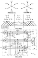
- FIG. 3 there is shown a conceptual or block diagram of a frequency controlled oscillator 110, using single-ended operation.
- Each of the three phasors C1-C3 from the ring oscillator 102 is buffered by an inverting and non-inverting driver 120-124 in FCO 110, to generate six equally phase spaced phasors: C1_P, C1_N, C2_P, C2_N, C3_P, and C3_N.
- each of the three low frequency phasors P1-P3 from the waveform synthesizer 104 is buffered by an analog inverting and non-inverting amplifier 130-134 to generate six equally phase spaced phasors: P1_P, P1_N, P2_P, P2_N, P3_P and P3_N.
- the six high frequency phasors are amplitude modulated, using modulators M1 through M6, by corresponding ones of the low frequency phasors.
- the resulting modulated signals are then combined by a summing circuit 140 to generate an output signal F OUT whose frequency f OUT is equal to f0 + f M or f0 - f M .
- a change in frequency or phase shift in the control signals P1-P3 results in an equal change in F OUT , allowing the FCO to replace a traditional VCO.
- the summing circuit 140 includes a bandpass filter (shown as element 222 in Figure 6) centered at frequency f0 to reject the dc component of the summed clock signal and also to reject any switching glitches caused by the stepped triangular shape of the control waveforms P1-P3.
- a bandpass filter shown as element 222 in Figure 6
- Figure 4A shows that the high frequency phasors C1_P, C1_N, C2_P, C2_N, C3_P and C3_N are equally phase spaced phasors, each spaced 60 degrees from its neighbor. Similarly, the control phasors P1_P, P1_N, P2_P, P2_N, P3_P and P3_N are also equally phase spaced.
- the timing diagram of Figure 5 shows the phase relationships of the phase control signals P1_P, P2_P and P3_P generated by the waveform synthesizer 104, which depends on whether the frequency f IN of the input signal is greater than, equal, or less than the reference frequency f0.
- P1_P is made to lead P2_P
- P2_P is made to lead P3_P, as shown at the left side of the timing diagram, which causes f OUT to equal f0 - f M .
- the circuitry in the FCO 110 of the preferred embodiment employs ECL circuit components.
- the termination resistors of ECL gates are omitted in these figures.
- each buffer 120-124 has dual complementary output lines, which for buffer 120 are labelled 200-206.
- Two of the output lines 204 and 206 are coupled by resistors to the "+" side (line 226) of a differential driver 210 (e.g. the F100114 made by National Semiconductor) and two of the output lines 200 and 202 are coupled to the "-" side (line 224) of the driver 210.
- the signals on the "+” and “-" sides of driver 210 are simply mirror images of one another. As a result, the differential input signal to the driver 210 is twice as large as it would be if single-ended operation were being used.
- All of the high frequency clock lines 200-206 are coupled to the control signal circuits that generate the P1, P2 and P3 signals by separate 220 ohm resistors.
- the open-emitter output stage of buffers 120-124 e.g., F100113 buffers made by National Semiconductor
- the 220 ohm emitter resistors form twelve amplitude modulators for modulating the low frequency control signals onto the high frequency reference signals.
- Each clock signal line is coupled to a differential resistive summing circuit 140, which has a separate 51 ohm driving resistor for each modulated clock line.
- the summing circuit 140 includes a bandpass filter 222 (equivalent to the LC circuit shown in Figure 6, but implemented on an integrated circuit using standard active filter techniques) centered at frequency f0 to reject the dc component as well as unwanted harmonics of the summed clock signal.
- the summed and filtered clock signals on lines 224 and 226, which are mirror images of one another, are amplified by a differential driver 210, and then buffered by a buffer stage 230 that outputs a clock signal PLL_CLK and its complement PLL_CLK_N, each of which is a periodic signal having a frequency of f0 + f M or f0 - f M .
- the P1_P signal modulates the C1_P signal on line 204
- the P1_N signal modulates the C1_N signal on line 206.
- Amplitude modulation is accomplished simply by applying a time varying voltage to the high frequency signals C1_P and C1_N through a 220 ohm resistor.
- FIG. 7 there is shown a circuit diagram of a circuit 250 for converting one phasor P1 of a three phase control signal into a two modulation signals P1_P and P1_N.
- Three copies of circuit 250 are used to convert control signals P1, P2 and P3 into six phasor control signals P1_P, P1_N, P2_P, P2_N, P3_P and P3_N.
- the circuit 250 has two stages 252 and 254, with the output signal P1_P of the first stage driving the second stage 254.
- Each stage has an amplifier 256 that drives the base of a PNP transistor 258.
- the output line 260 of each stage is coupled to the emitter of the corresponding PNP transistor 258.
- the first stage 252 is a level shifter and inverting attenuator, converting the 0 to 5 volt range (typical of TTL circuits) of the triangular P1 signal, to the -1 to -2 volt range used in ECL circuits.
- the second stage 254 is a simple inverting amplifier.
- the number of phases could by any value of 2N, where N is a positive odd integer, such as 6 (as in the preferred embodiment), 10, 14 and so on.
- a primary advantage of the using a 2N phase signal is that the odd number of N phasors with their complementary signals automatically eliminate unwanted harmonics, especially the third harmonic of the control signal, and theoretically generates a single spectra with frequency equal to the sum or the difference of f0 and f M , as controlled by the phase relationship among the control signals.
- the high frequency and low frequency clock signals are represented by the following formulas: w0 is the angular frequency of the three-phase reference clock signals. W M is the angular frequency of the three-phase control signals.
- ANALYSIS B Using Square Wave Clock and Triangular Control Signals
- the reference clock phasors are square waves at angular frequency w0, with a duty cycle of 50%, peak amplitude of ⁇ 0.5 and dc offset of K1.
- the 3-phase control signals P1_P, etc. are triangular waves at angular frequency W M , with amplitude ⁇ 0.5K3 and dc offset of K2.
- the following equation for the output clock F OUT can be derived for cases A1 and A2 of Analysis A: The DC component of F OUT is removed by the bandpass filter 222 in the summing circuit 140.
- the third harmonic of f M present in the control signal phasors (i.e., the w0 ⁇ 3w M component of the P1, P2 and P3 signals) is canceled out when all the modulated signal components are summed, and the next harmonic that is present in the summed signal (i.e., the w0 ⁇ 5w M component) has only 4% of the amplitude of the main F OUT signal component.
- the use of an odd number of clock and triangular control phasors and their complements (i.e., 2N phasors where N is an odd integer) in the FCO generates a high frequency PLL clock signal with acceptable granularity.
Applications Claiming Priority (2)
| Application Number | Priority Date | Filing Date | Title |
|---|---|---|---|
| US07/703,404 US5132633A (en) | 1991-05-21 | 1991-05-21 | PLL using a multi-phase frequency correction circuit in place of a VCO |
| US703404 | 1991-05-21 |
Publications (3)
| Publication Number | Publication Date |
|---|---|
| EP0515074A2 true EP0515074A2 (fr) | 1992-11-25 |
| EP0515074A3 EP0515074A3 (en) | 1993-05-05 |
| EP0515074B1 EP0515074B1 (fr) | 1996-03-20 |
Family
ID=24825247
Family Applications (1)
| Application Number | Title | Priority Date | Filing Date |
|---|---|---|---|
| EP92304276A Expired - Lifetime EP0515074B1 (fr) | 1991-05-21 | 1992-05-12 | Oscillateur contrÔlé en fréquence pour une boucle à verrouillage de phase haute fréquence |
Country Status (5)
| Country | Link |
|---|---|
| US (1) | US5132633A (fr) |
| EP (1) | EP0515074B1 (fr) |
| JP (1) | JPH05227020A (fr) |
| KR (1) | KR100219871B1 (fr) |
| DE (1) | DE69209143T2 (fr) |
Cited By (5)
| Publication number | Priority date | Publication date | Assignee | Title |
|---|---|---|---|---|
| WO1999023755A1 (fr) * | 1997-10-31 | 1999-05-14 | Telefonaktiebolaget Lm Ericsson | Amplificateur de puissance rf lineaire comportant des commutateurs a activation optique |
| EP1022857A2 (fr) * | 1999-01-25 | 2000-07-26 | Sun Microsystems, Inc. | Boucle à verrouillage de phase et procédé produisant un cadencement redondant de secours |
| WO2001084702A2 (fr) * | 2000-04-28 | 2001-11-08 | Broadcom Corporation | Systemes emetteurs-recepteurs tres rapides de donnees serie et procedes apparentes |
| US7245638B2 (en) | 2000-07-21 | 2007-07-17 | Broadcom Corporation | Methods and systems for DSP-based receivers |
| US7564866B2 (en) | 2000-07-21 | 2009-07-21 | Broadcom Corporation | Methods and systems for digitally processing optical data signals |
Families Citing this family (26)
| Publication number | Priority date | Publication date | Assignee | Title |
|---|---|---|---|---|
| JP3121448B2 (ja) * | 1991-09-06 | 2000-12-25 | ゼロックス コーポレイション | クロック発生回路 |
| US5402443A (en) * | 1992-12-15 | 1995-03-28 | National Semiconductor Corp. | Device and method for measuring the jitter of a recovered clock signal |
| US5347234A (en) | 1993-03-26 | 1994-09-13 | International Business Machines Corp. | Digital voltage controlled oscillator |
| JP3487309B2 (ja) | 1993-06-30 | 2004-01-19 | 株式会社ルネサステクノロジ | 半導体集積回路装置 |
| EP0657991B1 (fr) * | 1993-12-09 | 1997-11-05 | Hitachi, Ltd. | Circuit de détection de signaux pour une régulation digitale |
| KR970002949B1 (ko) * | 1994-05-25 | 1997-03-13 | 삼성전자 주식회사 | 디지탈 통신시스템의 클럭발생방법 및 그 회로 |
| EP0691733A2 (fr) * | 1994-07-08 | 1996-01-10 | Victor Company Of Japan, Ltd. | Circuit de conversion de fréquence |
| US5999571A (en) * | 1995-10-05 | 1999-12-07 | Silicon Image, Inc. | Transition-controlled digital encoding and signal transmission system |
| US5825824A (en) * | 1995-10-05 | 1998-10-20 | Silicon Image, Inc. | DC-balanced and transition-controlled encoding method and apparatus |
| US5974464A (en) * | 1995-10-06 | 1999-10-26 | Silicon Image, Inc. | System for high speed serial video signal transmission using DC-balanced coding |
| US5652533A (en) * | 1995-10-19 | 1997-07-29 | National Semiconductor Corporation | Circuit for generating sampling signals at closely spaced time intervals |
| US5656959A (en) * | 1995-11-24 | 1997-08-12 | International Microcircuits, Inc. | Clock synthesizer dual function pin system and method therefor |
| US5708383A (en) * | 1996-04-26 | 1998-01-13 | Nat Semiconductor Corp | Integrated circuit frequency controlled modulator for use in a phase lock loop |
| KR100475316B1 (ko) * | 1997-09-04 | 2005-03-10 | 실리콘 이미지, 인크.(델라웨어주 법인) | 피크 주파수들에서의 감소된 전자기 간섭을 위한 다수의동기화된 신호들의 제어 가능 딜레이들 |
| US6385442B1 (en) * | 1998-03-04 | 2002-05-07 | Symbol Technologies, Inc. | Multiphase receiver and oscillator |
| GB2362045B (en) * | 2000-02-23 | 2004-05-05 | Phoenix Vlsi Consultants Ltd | Analogue-Controlled phase interpolator |
| WO2001093443A2 (fr) * | 2000-05-26 | 2001-12-06 | Xtremespectrum, Inc. | Generateur de temporisation a haute resolution et basse puissance pour systemes de communications a largeur de bande ultralarge |
| US8311074B2 (en) | 2000-10-10 | 2012-11-13 | Freescale Semiconductor, Inc. | Low power, high resolution timing generator for ultra-wide bandwidth communication systems |
| US20030198311A1 (en) * | 2002-04-19 | 2003-10-23 | Wireless Interface Technologies, Inc. | Fractional-N frequency synthesizer and method |
| FR2895603B1 (fr) * | 2005-12-22 | 2009-10-30 | Valeo Securite Habitacle Sas | Procede et systeme de communication basse frequence |
| US8041310B2 (en) * | 2007-10-01 | 2011-10-18 | Telefonaktiebolaget Lm Ericsson (Publ) | Apparatus and methods for frequency control in a multi-output frequency synthesizer |
| WO2011071544A1 (fr) * | 2009-12-11 | 2011-06-16 | Ess Technology, Inc. | Générateur de fréquence numérique |
| CN102684654B (zh) | 2012-04-20 | 2014-12-10 | 华为技术有限公司 | 时钟信号发生器 |
| JP5971102B2 (ja) * | 2012-12-06 | 2016-08-17 | 富士通株式会社 | クロック位相調整回路および受信回路 |
| US9485049B2 (en) * | 2013-03-29 | 2016-11-01 | Infinera Corporation | Adjusting carrier spacing in a channel |
| KR102292644B1 (ko) | 2013-12-24 | 2021-08-23 | 삼성전자주식회사 | 고속으로 동작하는 이미지 센서 |
Citations (4)
| Publication number | Priority date | Publication date | Assignee | Title |
|---|---|---|---|---|
| US2881320A (en) * | 1957-06-07 | 1959-04-07 | Goldberg Bernard | Variable frequency high stability oscillator |
| US3151915A (en) * | 1961-06-05 | 1964-10-06 | Lear Siegler Inc | Apparatus for obtaining the sum or difference of the frequencies of two alternating signals |
| JPS5972234A (ja) * | 1982-10-18 | 1984-04-24 | Nippon Telegr & Teleph Corp <Ntt> | 位相同期発振回路 |
| GB2183946A (en) * | 1985-12-06 | 1987-06-10 | Plessey Co Plc | Frequency synthesiser |
Family Cites Families (2)
| Publication number | Priority date | Publication date | Assignee | Title |
|---|---|---|---|---|
| US5059924A (en) * | 1988-11-07 | 1991-10-22 | Level One Communications, Inc. | Clock adapter using a phase locked loop configured as a frequency multiplier with a non-integer feedback divider |
| US5068628A (en) * | 1990-11-13 | 1991-11-26 | Level One Communications, Inc. | Digitally controlled timing recovery loop |
-
1991
- 1991-05-21 US US07/703,404 patent/US5132633A/en not_active Expired - Lifetime
-
1992
- 1992-05-12 DE DE69209143T patent/DE69209143T2/de not_active Expired - Lifetime
- 1992-05-12 EP EP92304276A patent/EP0515074B1/fr not_active Expired - Lifetime
- 1992-05-20 JP JP4127812A patent/JPH05227020A/ja active Pending
- 1992-05-20 KR KR1019920008489A patent/KR100219871B1/ko not_active IP Right Cessation
Patent Citations (4)
| Publication number | Priority date | Publication date | Assignee | Title |
|---|---|---|---|---|
| US2881320A (en) * | 1957-06-07 | 1959-04-07 | Goldberg Bernard | Variable frequency high stability oscillator |
| US3151915A (en) * | 1961-06-05 | 1964-10-06 | Lear Siegler Inc | Apparatus for obtaining the sum or difference of the frequencies of two alternating signals |
| JPS5972234A (ja) * | 1982-10-18 | 1984-04-24 | Nippon Telegr & Teleph Corp <Ntt> | 位相同期発振回路 |
| GB2183946A (en) * | 1985-12-06 | 1987-06-10 | Plessey Co Plc | Frequency synthesiser |
Non-Patent Citations (1)
| Title |
|---|
| PATENT ABSTRACTS OF JAPAN vol. 8, no. 181 (E-261)(1618) 21 August 1984 & JP-A-59 72 234 ( NIPPON DENSHI DENWA KOSHA ) 24 April 1984 * |
Cited By (20)
| Publication number | Priority date | Publication date | Assignee | Title |
|---|---|---|---|---|
| WO1999023755A1 (fr) * | 1997-10-31 | 1999-05-14 | Telefonaktiebolaget Lm Ericsson | Amplificateur de puissance rf lineaire comportant des commutateurs a activation optique |
| US6385439B1 (en) | 1997-10-31 | 2002-05-07 | Telefonaktiebolaget Lm Ericsson (Publ) | Linear RF power amplifier with optically activated switches |
| EP1022857A3 (fr) * | 1999-01-25 | 2003-08-27 | Sun Microsystems, Inc. | Boucle à verrouillage de phase et procédé produisant un cadencement redondant de secours |
| EP1022857A2 (fr) * | 1999-01-25 | 2000-07-26 | Sun Microsystems, Inc. | Boucle à verrouillage de phase et procédé produisant un cadencement redondant de secours |
| US8223828B2 (en) | 2000-04-28 | 2012-07-17 | Broadcom Corporation | Methods and systems for adaptive receiver equalization |
| WO2001084702A2 (fr) * | 2000-04-28 | 2001-11-08 | Broadcom Corporation | Systemes emetteurs-recepteurs tres rapides de donnees serie et procedes apparentes |
| US6791388B2 (en) | 2000-04-28 | 2004-09-14 | Broadcom Corporation | Phase interpolator device and method |
| US6995594B2 (en) | 2000-04-28 | 2006-02-07 | Broadcom Corporation | Phase interpolator device and method |
| WO2001084702A3 (fr) * | 2000-04-28 | 2002-06-06 | Broadcom Corp | Systemes emetteurs-recepteurs tres rapides de donnees serie et procedes apparentes |
| US7286597B2 (en) | 2000-04-28 | 2007-10-23 | Broadcom Corporation | Methods and systems for adaptive receiver equalization |
| US8824538B2 (en) | 2000-04-28 | 2014-09-02 | Broadcom Corporation | Methods and systems for adaptive receiver equalization |
| EP2104232A2 (fr) * | 2000-04-28 | 2009-09-23 | Broadcom Corporation | Interpolateur de phase pour un système de transmission et réception pour la transmission sérielle et méthode |
| EP2104232A3 (fr) * | 2000-04-28 | 2009-10-14 | Broadcom Corporation | Interpolateur de phase pour un système de transmission et réception pour la transmission sérielle et méthode |
| US8798219B2 (en) | 2000-04-28 | 2014-08-05 | Broadcom Corporation | High-speed serial data transceiver and related methods |
| US8472512B2 (en) | 2000-04-28 | 2013-06-25 | Broadcom Corporation | Methods and systems for adaptive receiver equalization |
| US7245638B2 (en) | 2000-07-21 | 2007-07-17 | Broadcom Corporation | Methods and systems for DSP-based receivers |
| US8363683B2 (en) | 2000-07-21 | 2013-01-29 | Broadcom Corporation | Methods and systems for DSP-based receivers |
| US7835387B2 (en) | 2000-07-21 | 2010-11-16 | Broadcom Corporation | Methods and systems for digitally processing data signals |
| US7778286B2 (en) | 2000-07-21 | 2010-08-17 | Broadcom Corporation | Methods and systems for DSP-based receivers |
| US7564866B2 (en) | 2000-07-21 | 2009-07-21 | Broadcom Corporation | Methods and systems for digitally processing optical data signals |
Also Published As
| Publication number | Publication date |
|---|---|
| DE69209143T2 (de) | 1996-08-29 |
| EP0515074B1 (fr) | 1996-03-20 |
| JPH05227020A (ja) | 1993-09-03 |
| EP0515074A3 (en) | 1993-05-05 |
| DE69209143D1 (de) | 1996-04-25 |
| US5132633A (en) | 1992-07-21 |
| KR100219871B1 (ko) | 1999-09-01 |
| KR920022684A (ko) | 1992-12-19 |
Similar Documents
| Publication | Publication Date | Title |
|---|---|---|
| US5132633A (en) | PLL using a multi-phase frequency correction circuit in place of a VCO | |
| US5790614A (en) | Synchronized clock using a non-pullable reference oscillator | |
| Razavi | Design of monolithic phase-locked loops and clock recovery circuits-A tutorial | |
| EP0538903B1 (fr) | Synthèse de fréquence utilisant une porteuse contrÔlée en fréquence et modulée par le signal de réaction d'une boucle à verrouillage de phase | |
| JP2993200B2 (ja) | 位相同期ループ | |
| EP0800276B1 (fr) | Circuit multiplicateur de fréquence avec un étage d'entrée ayant un facteur multiplicatif supérieur à celui des étages suivantes | |
| CA1161127A (fr) | Boucle a asservissement de phase stabilisee par un oscillateur a cristal | |
| US20040001600A1 (en) | Phase locked loop circuit for reducing electromagnetic interference and contorl method thereof | |
| US5187722A (en) | Frequency synthesis using fractional frequency multiplication | |
| WO1998036491A1 (fr) | Multiplicateur de frequence d'oscillateur en anneau commande en tension | |
| US4303893A (en) | Frequency synthesizer incorporating digital frequency translator | |
| US3546617A (en) | Digital frequency synthesizer | |
| US5710524A (en) | Clock synthesizer for low EMI applications | |
| JPH0645930A (ja) | 周波数シンセサイザ | |
| EP0203756A2 (fr) | Synthétiseurs de fréquence | |
| JP3712141B2 (ja) | 位相同期ループ装置 | |
| KR960012922B1 (ko) | 주파수 편이 키잉 변조기 | |
| JPS58168333A (ja) | 位相同期ル−プ回路の位相比較方式 | |
| JP2619663B2 (ja) | フェーズ・ロックド・ループ | |
| JP2000004121A (ja) | 発振変調回路 | |
| JPS61216529A (ja) | 誘導無線周波数シンセサイザ装置 | |
| JP2577933B2 (ja) | フェーズ・ロックド・ループ | |
| KR0123182Y1 (ko) | 위상동기 루프회로의 동기시간 최소화장치 | |
| KR930004859B1 (ko) | 위상 고정 루프 회로의 위상 검출장치 | |
| JPH08279716A (ja) | 角度変調回路 |
Legal Events
| Date | Code | Title | Description |
|---|---|---|---|
| PUAI | Public reference made under article 153(3) epc to a published international application that has entered the european phase |
Free format text: ORIGINAL CODE: 0009012 |
|
| AK | Designated contracting states |
Kind code of ref document: A2 Designated state(s): DE FR GB IT NL |
|
| PUAL | Search report despatched |
Free format text: ORIGINAL CODE: 0009013 |
|
| AK | Designated contracting states |
Kind code of ref document: A3 Designated state(s): DE FR GB IT NL |
|
| 17P | Request for examination filed |
Effective date: 19931029 |
|
| 17Q | First examination report despatched |
Effective date: 19940110 |
|
| GRAA | (expected) grant |
Free format text: ORIGINAL CODE: 0009210 |
|
| AK | Designated contracting states |
Kind code of ref document: B1 Designated state(s): DE FR GB IT NL |
|
| PG25 | Lapsed in a contracting state [announced via postgrant information from national office to epo] |
Ref country code: IT Free format text: LAPSE BECAUSE OF FAILURE TO SUBMIT A TRANSLATION OF THE DESCRIPTION OR TO PAY THE FEE WITHIN THE PRE;WARNING: LAPSES OF ITALIAN PATENTS WITH EFFECTIVE DATE BEFORE 2007 MAY HAVE OCCURRED AT ANY TIME BEFORE 2007. THE CORRECT EFFECTIVE DATE MAY BE DIFFERENT FROM THE ONE RECORDED.SCRIBED TIME-LIMIT Effective date: 19960320 Ref country code: FR Effective date: 19960320 Ref country code: NL Free format text: LAPSE BECAUSE OF FAILURE TO SUBMIT A TRANSLATION OF THE DESCRIPTION OR TO PAY THE FEE WITHIN THE PRESCRIBED TIME-LIMIT Effective date: 19960320 |
|
| REF | Corresponds to: |
Ref document number: 69209143 Country of ref document: DE Date of ref document: 19960425 |
|
| PG25 | Lapsed in a contracting state [announced via postgrant information from national office to epo] |
Ref country code: GB Effective date: 19960620 |
|
| EN | Fr: translation not filed | ||
| NLV1 | Nl: lapsed or annulled due to failure to fulfill the requirements of art. 29p and 29m of the patents act | ||
| PLBE | No opposition filed within time limit |
Free format text: ORIGINAL CODE: 0009261 |
|
| STAA | Information on the status of an ep patent application or granted ep patent |
Free format text: STATUS: NO OPPOSITION FILED WITHIN TIME LIMIT |
|
| GBPC | Gb: european patent ceased through non-payment of renewal fee |
Effective date: 19960620 |
|
| 26N | No opposition filed | ||
| PGFP | Annual fee paid to national office [announced via postgrant information from national office to epo] |
Ref country code: DE Payment date: 20110527 Year of fee payment: 20 |
|
| REG | Reference to a national code |
Ref country code: DE Ref legal event code: R071 Ref document number: 69209143 Country of ref document: DE |
|
| REG | Reference to a national code |
Ref country code: DE Ref legal event code: R071 Ref document number: 69209143 Country of ref document: DE |
|
| PG25 | Lapsed in a contracting state [announced via postgrant information from national office to epo] |
Ref country code: DE Free format text: LAPSE BECAUSE OF EXPIRATION OF PROTECTION Effective date: 20120515 |