EP0504984A2 - Verfahren zur Herstellung von einer Verbindung über einer Halbleitervorrichtung - Google Patents
Verfahren zur Herstellung von einer Verbindung über einer Halbleitervorrichtung Download PDFInfo
- Publication number
- EP0504984A2 EP0504984A2 EP92200697A EP92200697A EP0504984A2 EP 0504984 A2 EP0504984 A2 EP 0504984A2 EP 92200697 A EP92200697 A EP 92200697A EP 92200697 A EP92200697 A EP 92200697A EP 0504984 A2 EP0504984 A2 EP 0504984A2
- Authority
- EP
- European Patent Office
- Prior art keywords
- layer
- electrically conductive
- activating layer
- side wall
- opening
- Prior art date
- Legal status (The legal status is an assumption and is not a legal conclusion. Google has not performed a legal analysis and makes no representation as to the accuracy of the status listed.)
- Granted
Links
Images
Classifications
-
- H—ELECTRICITY
- H10—SEMICONDUCTOR DEVICES; ELECTRIC SOLID-STATE DEVICES NOT OTHERWISE PROVIDED FOR
- H10P—GENERIC PROCESSES OR APPARATUS FOR THE MANUFACTURE OR TREATMENT OF DEVICES COVERED BY CLASS H10
- H10P50/00—Etching of wafers, substrates or parts of devices
- H10P50/60—Wet etching
- H10P50/66—Wet etching of conductive or resistive materials
- H10P50/663—Wet etching of conductive or resistive materials by chemical means only
- H10P50/667—Wet etching of conductive or resistive materials by chemical means only by liquid etching only
-
- H—ELECTRICITY
- H10—SEMICONDUCTOR DEVICES; ELECTRIC SOLID-STATE DEVICES NOT OTHERWISE PROVIDED FOR
- H10P—GENERIC PROCESSES OR APPARATUS FOR THE MANUFACTURE OR TREATMENT OF DEVICES COVERED BY CLASS H10
- H10P50/00—Etching of wafers, substrates or parts of devices
- H10P50/20—Dry etching; Plasma etching; Reactive-ion etching
- H10P50/26—Dry etching; Plasma etching; Reactive-ion etching of conductive or resistive materials
- H10P50/264—Dry etching; Plasma etching; Reactive-ion etching of conductive or resistive materials by chemical means
-
- H—ELECTRICITY
- H10—SEMICONDUCTOR DEVICES; ELECTRIC SOLID-STATE DEVICES NOT OTHERWISE PROVIDED FOR
- H10W—GENERIC PACKAGES, INTERCONNECTIONS, CONNECTORS OR OTHER CONSTRUCTIONAL DETAILS OF DEVICES COVERED BY CLASS H10
- H10W20/00—Interconnections in chips, wafers or substrates
- H10W20/01—Manufacture or treatment
- H10W20/031—Manufacture or treatment of conductive parts of the interconnections
- H10W20/056—Manufacture or treatment of conductive parts of the interconnections by filling conductive material into holes, grooves or trenches
- H10W20/057—Manufacture or treatment of conductive parts of the interconnections by filling conductive material into holes, grooves or trenches by selectively depositing, e.g. by using selective CVD or plating
Definitions
- This invention relates to a method of manufacturing a semiconductor device, which method comprises providing a semiconductor body having at a major surface a surface structure comprising an insulating layer through which is formed an opening defining a side wall of insulating material bounding an exposed surface area of a region beneath the insulating layer, providing an activating layer on the exposed surface area and the side wall of the opening, and depositing electrically conductive material to form an electrical region in the opening in electrical contact with the underlying region.
- US-A-4822753 describes such a method.
- the opening in the insulating layer exposes a silicide surface area of a silicon device region and the activating layer is provided by blanket depositing a layer of titanium nitride over the insulating layer.
- a levelling or planarising agent such as a spin-on-glass is then applied over the surface to fill the opening.
- the levelling agent is then etched anisotropically to leave the levelling agent only in the opening.
- the activating or nucleating layer is then etched using the levelling agent as a mask so as to remove the exposed areas of the activating layer.
- the titanium nitride activating layer provides a nucleation surface for the selective deposition of tungsten to form the electrically conductive material region or plug in electrical contact with the underlying region exposed by the opening.
- the levelling agent acts as an etch mask to enable the portion of the activating layer in the surface of the insulating layer to be removed.
- the side wall of the opening remains covered by the activating layer after removal of the remaining levelling agent. Accordingly, nucleation sites for the electrically conductive material are provided not only on the surface area to be contacted but also on the side wall of the opening so that the electrically conductive material may be deposited on and thus 'grow' from the side wall as well as the surface area.
- Such side wall growth of the electrically conductive material may result in voids or spaces in the electrically conductive region or plug which may detrimentally affect the quality of the electrical contact to the underlying region.
- a method of manufacturing a semiconductor device comprises providing a semiconductor body having at a major surface a surface structure comprising an insulating layer through which is formed an opening defining a side wall of insulating material bounding an exposed surface area of a region beneath the insulating layer, providing an activating layer on the exposed surface area and the side wall of the opening, and depositing electrically conductive material on the activating layer to form an electrically conductive region in the opening in electrical contact with the underlying region, characterised by providing the activating layer so that the activating layer material on the side wall has different characteristics from the activating layer material on the exposed surface area and selectively etching the activating layer to remove the activating layer material from the side wall of the opening before depositing the electrically conductive material.
- the activating layer is provided in such a manner that the portion of the activating layer on the side wall of the opening can be selectively etched with respect to the portion on the surface area of the underlying region so enabling the side wall portion of the activating layer to be removed.
- the activating layer portion on the surface area of the underlying region remains so that deposition of the electrical material occurs on the activating layer to cause 'growth' of the electrically conductive upwards from the surface area. Little or no deposition of the electrically conductive material occurs on the opening side wall so inhibiting side ways growth of the electrically conductive material and thus avoiding or at least reducing the possibility of voids being formed in the electrically conductive region.
- such a method is not reliant on the properties of the surface area to be contacted.
- the present method does not rely on the surface area to enable selective deposition of the activating layer onto only the surface area.
- the activating layer is provided on the surface area and the side wall of the opening and then selectively removed from the side wall.
- This enables the surface area to be, for example, a metal, a silicide or a silicon surface area and, especially in the case of contact areas or contact holes for enabling electrical contact to semiconductor device regions, allows formation of the electrically conductive region even where the opening extends (due, for example, to misalignment) onto an insulating region adjacent the region to be contacted.
- the activating layer may be provided on the exposed surface area and the side wall of the opening by depositing the activating layer over the insulating layer and then removing the activating layer from the top surface of the insulating layer.
- the portion of the activating layer on the top surface of the insulating layer may be removed by polishing which avoids the need for a photosensitive resist or other mask layer. This provides a simple way of removing the top surface portion of the activating layer without the need for resist or other masks.
- a mask for example a photosensitive resist mask, could be used to enable removal of the top surface portion of the activating layer.
- the activating layer is of titanium-tungsten alloy provided by sputtering.
- the present inventor has found that when a titanium-tungsten alloy is deposited by sputtering, the composition of the alloy on the surface area which is generally transverse to the direction of sputtering differs from the composition of the alloy on the side wall which lies generally in the direction of sputtering and, in particular, that the portion of the titanium-tungsten alloy on the opening side wall is comparatively rich in titanium.
- the relatively light titanium atoms are far more susceptible to scattering by collision with gas atoms in the sputtering plasma than are the relatively heavy tungsten atoms. Accordingly, the tungsten atoms will tend to be sputtered directly towards the substrate whereas the titanium atoms will be scattered. Accordingly the alloy deposited on surfaces which are transverse to the sputtering direction will be rich in tungsten whilst the alloy deposited on surfaces which lie generally in the direction of sputtering will be rich in titanium.
- the fact that the composition of the alloy on the side wall is different from that of the alloy on the surface area results in the alloy on the side wall having different characteristics from the alloy on the surface area enabling the alloy on the surface area to be etched selectively.
- the titanium-rich portion may be removed by using hot phosphoric acid or possibly dilute hydrofluoric acid.
- the use of a method in accordance with the invention enables the use of aluminium and the attendant problems of electromigration to be avoided because the electrically conductive material may be deposited by an electroless deposition technique and may be for example gold, copper or nickel.
- electrically conductive material may be deposited onto the activating layer using a selective chemical vapour deposition technique.
- tungsten may be selectively deposited onto the activating layer.
- the activating layer may also serve to provide a barrier to contamination of the exposed surface area by the subsequent metallisation. This may be especially important where the metallisation contains copper.
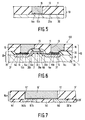
- FIG. 6 there is illustrated a method of manufacturing a semiconductor device 100 ( Figure 6) which method comprises providing a semiconductor body 1 ( Figure 6) having at a major surface 2 a surface structure 10 comprising an insulating layer 11 through which is formed an opening 12 defining a side wall 13 of insulating material bounding an exposed surface area 14a of a region 14 ( Figure 6) beneath the insulating layer 11, providing an activating layer 15 on the exposed surface area 14a and the side wall 13 of the opening 12, and depositing electrically conductive material on the activating layer 15 to form an electrically conductive region 16 in the opening 12 and in electrical contact with the underlying region 14.
- the method further comprises providing the activating layer 15 so that the activating layer material 15a on the side wall 13 has different characteristics from the activating layer material 15b on the exposed surface area 14a and selectively etching the activating layer to remove the activating layer material 15a from the side wall 13 of the opening 12 before depositing the electrically conductive material.
- the activating layer 15 is thus provided in such a manner that the portion 15a of the activating layer on the side wall 13 of the opening 12 can be selectively etched with respect to the portion 15b on the surface area 14a of the underlying region so enabling the side wall portion 15b of the activating layer to be removed.
- the activating layer portion 15b on the surface area 14a of the underlying region remains so that deposition of the electrical material occurs on the activating layer portion 15b to cause 'growth' of the electrically conductive upwards from the surface area. Little or no deposition of the electrically conductive material occurs on the opening side wall 13, so inhibiting side ways growth of the electrically conductive material and thus avoiding or at least reducing the possibility of voids being formed in the electrically conductive region.
- this method is not reliant on the properties of the surface area 14a to be contacted.
- the method does not rely on the characteristics of the surface area 14a to enable selective deposition of the activating layer 15 onto only the surface area 14a.
- the activating layer 15 is provided on the surface area 14a and the side wall 13 of the opening 12 and then selectively removed from the side wall 13.
- This enables the surface area 14a to be, for example, a metal, a silicide or a silicon surface area and moreover allows, especially in the case of contact areas or contact holes to semiconductor device regions, formation of the electrically conductive region even where the opening extends (due, for example, to misalignment) onto insulating regions adjacent the region to be contacted.
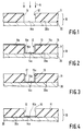
- Figure 1 illustrates a surface structure 10 of a semiconductor body.
- the surface structure 10 comprises the insulating layer 11 which may be, for example, a silicon oxide layer deposited by chemical vapour deposition a TEOS (tetraethylorthosilicate) layer or any other suitable insulating material such as a silicon nitride layer and is provided on a surface 20a of the remaining portion 20 of the surface structure 10.
- the remaining portion 20 of the surface structure 10 may comprise a surface region of the semiconductor body 1 ( Figure 6) at which is provided a doped region 14 to be electrically contacted or may comprise a region 140 of a metallisation level provided on the semiconductor body 1 ( Figure 7).
- the nature of the region 14 to be electrically contacted is not important and accordingly this region is not specifically shown in Figures 1 to 5 but is indicated merely by its surface area 14a.
- the opening 12 is formed in the insulating layer 11 using conventional photolithographic and etching techniques to expose the surface area 14a.
- the semiconductor body carrying the surface structure 10 is then placed in a conventional sputtering machine, for example a sputter machine produced by Oke of Japan and material is sputtered onto the surface structure 10 as indicated by the arrows A in Figure 1 to produce the activating layer 15 shown in Figure 2.
- the activating layer 15 is formed of a titanium-tungsten alloy by sputtering material from a target formed of a titanium-tungsten alloy. As shown in Figure 2 the activating layer 15 is at this state a blanket layer covering the top surface 11a of the insulating layer 11, the side wall 13 and the surface area 14a.
- a chemomechanical polishing process is then used to remove the portion 15c of the activating layer 15 present on the top surface 11a of the insulating layer 11.
- the polishing may be carried out using an abrasive slurry such as an alumina slurry in a commercial polishing machine as described in, for example, EP-A-223920.
- the polishing may be continued for a given time which may be determined experimentally.
- a polishing stop layer such as a layer of silicon nitride (see EP-A-223902) may be provided on top of the insulating layer 11 to provide better control of the end point of the polishing.
- the insulating layer 11 itself may be formed of silicon nitride which should assist in preventing diffusion of, for example, copper atoms and thus should assist in inhibiting contamination of the semiconductor body where copper is used for the metallisation.
- the activating layer 15 remains on the side wall 13 of the opening 12 as well as on the surface area 14a after completion of the polishing step.
- the activating layer 15 provides a surface to which the subsequently deposited electrically conductive material adheres preferentially.
- the activating layer 15 may provide nucleation sites for the growth of the electrically conductive material. If the portion 15a of the activating layer 15 remains on the side wall 13 of the opening 12, then 'growth' or deposition of the electrically conductive material will occur on both the side wall portion 15a and the surface area portion 15b of the activating layer 15.
- the electrically conductive material deposited on the side wall 13 of the opening may meet or join together preventing further deposition at the surface area 14a and thus resulting in voids or spaces in the electrically conductive material. Such voids or spaces may detrimentally affect the quality of the electrical contact to the underlying region 14.
- the portion 15a of the activating layer 15 on the side wall 13 should be removed.
- the present inventor has found that, when a titanium-tungsten alloy is deposited by sputtering, the composition of the portion 15b of the titanium-tungsten alloy on the surface area 14a which is generally transverse, as shown perpendicular, to the direction of sputtering differs from the composition of the titanium-tungsten portion 15a of the alloy on the side wall 13 of the opening 12 which lies generally in the direction A of sputtering and, in particular, that the portion 15a of the titanium-tungsten alloy on the opening side wall 13 is comparatively rich in titanium.
- the relatively light titanium atoms are far more susceptible to scattering by collision with gas atoms in the sputtering plasma than are the relatively heavy tungsten atoms. Accordingly, the tungsten atoms will tend to be sputtered directly towards the substrate whereas the titanium atoms will be scattered.
- the alloy deposited on surfaces which are transverse to the sputtering direction will be rich in tungsten whilst the alloy deposited on surfaces which lie generally in the direction of sputtering will be rich in titanium.
- the composition of the portion 15a of the alloy on the side wall 13 is different from that of the portion 15b of the alloy on the surface area 14a results in the portion 15a having different characteristics from the portion 15b and enables the portion 15a to be etched selectively with respect to the portion 15b.
- the titanium rich portion 15a may be removed by using hot phosphoric acid or possibly dilute hydrofluoric acid to produce the structure shown in Figure 4.
- the activating layer portion 15b on the surface area 14a remains so that the subsequently deposited electrically conductive material which adheres or deposits preferentially on the activating layer portion 15b is deposited at the surface area 14a and 'grows' upwards to fill the opening 12.
- the possibility of voids or spaces being formed in the electrically conductive material is reduced.
- the selective etching process in accordance with the invention enables the side wall portion 15a of the activating layer 15 to be removed without the need for the use of mask. Also because the selective etching is determined by the different compositions of the alloy material deposited on the side wall 13 and the surface area 14a, the end point of the etching process is self-determining and relatively precise so avoiding or at least reducing the possible problems of under or over etching of the activating layer 15.
- Electrically conductive material is then deposited by, in this example, a conventional electroless deposition technique to form the electrically conductive region 16.
- a conventional electroless deposition technique to form the electrically conductive region 16.
- the presence of the activating layer 15b only on the surface area 14a enables a selective deposition technique to be used for forming the electrically conductive region.
- electrically conductive materials, such as copper which cannot easily be etched by the normally available methods such as plasma etching to be used. Accordingly, the use of aluminium and the attendant problems of electromigration can be avoided.
- the selective deposition technique may be an electroless plating technique.
- the electrically conductive material may be for example copper in which case an electroless plating solution of the type described in the paper entitled 'Copper as the future interconnection material' by P.L. Pai and C.H. Ting at page 258 et. seq. of the proceedings of the VMIC Conference in 1989 at Santa Clara, USA may be used.
- Electroless nickel may be deposited in place of copper using a similar electroless deposition technique.
- An example of an electroless nickel deposition solution is given in a paper by C.H. Ting and M. Paunovic entitled 'Selective Electroless Metal Deposition for integrated circuit fabrication' published in the Journal of the Electrochemical Society (J. Electrochem. Soc.) in Volume 136 No. 2 February 1989 at pages 456 to 461.
- the use of copper is, however, preferred because of its low resistivity.
- the electroless plating solution is an aqueous solution of an organic salt, nitrate or sulphate of the metal and in order to achieve precipitation of the metal from the solution onto the activating layer portion 15b, the alloy forming the metal to be deposited should have an ionisation potential smaller than that of the activating layer material.
- electrically conductive material may be deposited onto the activating layer 15 using a selective chemical vapour deposition technique.
- tungsten may be selectively deposited onto the titanium-tungsten activating layer 15.
- the activating layer portion 15b also serves as a barrier layer between the region 14 and the electrically conductive material region 16 to prevent or at least inhibit contamination of the region 14 by the electrically conductive material which is especially important where the electrically conductive material is or comprises copper.
- the method described above may be used to provide contact to any suitable region of a semiconductor device.
- the region may be, for example, a semiconductor device region, such as a source or drain region, or part of a lower metallisation level.
- Figure 6 illustrates part of a semiconductor device 1 in which a method in accordance with the invention has been used to make electrical connection to a semiconductor device region by enabling deposition of electrically conductive material into a contact hole.
- the semiconductor device comprises a monocrystalline silicon semiconductor body 30 having adjacent one major surface 2 a doped region 31 of one conductivity type, in this example p-conductivity type, within which more highly doped device regions 14 of the opposite conductivity type, in this example n-conductivity type, are provided adjacent the one major surface 2.
- the semiconductor body 1 will have many such device regions provided therein.
- the device regions 14 are associated with insulated gate structures 34 (only one being shown) provided on the one major surface 2 to form insulated gate field effect transistors (IGFETs).
- IGFETs insulated gate field effect transistors
- the semiconductor body may also contain p-channel IGFETs, so as to form a CMOS integrated circuit, with the p-channel IGFETs being formed by p-conductivity type device regions provided within an n-conductivity type well and, of course, associated insulated gates.
- the devices described above are formed in the semiconductor body 1 by, after definition of a field oxide pattern (part of an insulating region 35 of which is shown in Figure 6) by conventional local oxidation of silicon (LOCOS) techniques, forming the insulated gate structure 34 in conventional manner by growing a gate oxide layer on the surface 2 and then providing a doped polycrystalline silicon layer on the gate oxide layer.
- the doped polycrystalline silicon layer is locally capped by an insulating region 36a of, for example, silicon oxide and/or silicon nitride.
- lowly doped extension regions 14b of the device regions 14 are formed in self-aligned manner using the insulated gate structure 34 and the field oxide pattern 35 as a mask.
- a silicon oxide or silicon nitride layer is then deposited by a conventional chemical vapour deposition technique and etched using a suitable known anisotropic etching process to provide, as shown in Figure 6, insulating spacer regions 36b on the side walls of the insulated gate 34 which, together with the insulating capping region 36b, encapsulate the insulated gate 34to avoid undesired shorting by subsequent metallisation between the insulated gate 34 and a device region 14.
- other insulated gates of the device need not necessarily all be provided with a capping region 36a.
- More highly doped regions 14c of the device regions 14 are formed in conventional self-aligned manner using the insulated gate 34, spacer regions 36b and field oxide insulating regions 35as a mask.
- silicide regions 37 for example titanium or cobalt silicide, are formed at the surfaces of the device regions 14 in known manner by, for example, depositing a layer of titanium or cobalt and heating. This completes the portion 20 of the surface structure in this example.
- the insulating layer 11 is then provided as a layer of, in this example, silicon dioxide deposited by conventional CVD techniques.
- the surface structure 10 is thus completed.
- Figure 7 illustrates a situation where the portion 20' of the surface structure 10a comprises a metallisation level and the underlying region 140 forms part of that metallisation level.
- the regions 140 may be electrically conductive regions similar to the regions 16 shown in Figure 5 contacting semiconductor device regions 14 or may be part of a subsequent metallisation level.
- the regions 140 of the metallisation level are bounded by insulating material 14 and together with a covering insulating layer 11' form the surface structure 10a.
- the insulating 11' may be, for example, a silicon dioxide layer deposited by, for example, a chemical vapour deposition (CVD) technique or a TEOS layer or a silicon nitride layer.
- CVD chemical vapour deposition
- An opening 12' bounded by a side wall 13' is formed by conventional means in the insulating layer 11' and an activating layer portion 15'b and electrically conductive region 16' are formed in the manner described above with reference to Figures 1 to 5 to provide an electrical interconnection 16' between the regions 140.
- the activating layer portion 15'b need not make contact everywhere with the portion 20' and could, for example, extend up over the insulating layer 11 between the regions 140. The above described process may be repeated for further metallisation levels.
- the use of the activating layer portion 15b, 15'b to provide a nucleation layer for the electrically conductive material region 16,16' means that the selective deposition of the electrically conductive material is not dependent on the nature of the surface area 14a,140a and, accordingly, as illustrated in Figures 6 and 7, the opening 12,12' may, overlap onto an adjacent insulating region without significantly affecting the subsequent deposition of the electrically conductive material to form the electrically conductive region or plug 16,16'.
- the method is thus relatively tolerant of misalignment problems and facilitates the relatively close packing of active devices within the semiconductor device which is required for example VLSI devices.
- the activating layer 15 is formed of titanium-tungsten deposited by a sputtering technique
- the activating layer 15 may be formed of other suitable alloys and using any suitable deposition techniques in which one component of the alloy is lighter and thus more easily scattered by gas or other atoms present in the deposition chamber than another component of the alloy so that the composition of the deposited material varies depending on whether the surface on which the material is deposited is in the direction of or transverse to the direction of supply of the material to be deposited.
- the material deposited on the side wall which will be relatively rich in the one component should, of course, be capable of being selectively etched with respect to the material on the exposed surface area 14a which will be rich in the other component.
- the alloy may comprise additional components.
- III-V semiconductor devices such as gallium arsenide semiconductor devices.
Landscapes
- Internal Circuitry In Semiconductor Integrated Circuit Devices (AREA)
- Electrodes Of Semiconductors (AREA)
- Chemically Coating (AREA)
Applications Claiming Priority (2)
| Application Number | Priority Date | Filing Date | Title |
|---|---|---|---|
| GB9105943 | 1991-03-20 | ||
| GB919105943A GB9105943D0 (en) | 1991-03-20 | 1991-03-20 | A method of manufacturing a semiconductor device |
Publications (3)
| Publication Number | Publication Date |
|---|---|
| EP0504984A2 true EP0504984A2 (de) | 1992-09-23 |
| EP0504984A3 EP0504984A3 (en) | 1992-10-28 |
| EP0504984B1 EP0504984B1 (de) | 1997-06-18 |
Family
ID=10691918
Family Applications (1)
| Application Number | Title | Priority Date | Filing Date |
|---|---|---|---|
| EP92200697A Expired - Lifetime EP0504984B1 (de) | 1991-03-20 | 1992-03-11 | Verfahren zur Herstellung von einer Verbindung über einer Halbleitervorrichtung |
Country Status (6)
| Country | Link |
|---|---|
| US (1) | US5240879A (de) |
| EP (1) | EP0504984B1 (de) |
| JP (1) | JP2522879B2 (de) |
| KR (1) | KR100237096B1 (de) |
| DE (1) | DE69220399T2 (de) |
| GB (1) | GB9105943D0 (de) |
Cited By (3)
| Publication number | Priority date | Publication date | Assignee | Title |
|---|---|---|---|---|
| WO2000025984A1 (en) * | 1998-11-02 | 2000-05-11 | Applied Materials, Inc. | Chemical mechanical polishing a substrate having a filler layer and a stop layer |
| EP1081753A3 (de) * | 1999-08-30 | 2001-09-19 | Applied Materials, Inc. | Verfahren zur verbesserten Elektoplattierungsfüllung von Kontaktlöchern |
| EP1068928A3 (de) * | 1999-02-11 | 2003-08-13 | Applied Materials, Inc. | Chemisch-mechanisches Polierverfahren und Bauelemente |
Families Citing this family (18)
| Publication number | Priority date | Publication date | Assignee | Title |
|---|---|---|---|---|
| JP3211290B2 (ja) * | 1991-10-21 | 2001-09-25 | ソニー株式会社 | 半導体装置の形成方法 |
| US5474949A (en) * | 1992-01-27 | 1995-12-12 | Matsushita Electric Industrial Co., Ltd. | Method of fabricating capacitor or contact for semiconductor device by forming uneven oxide film and reacting silicon with metal containing gas |
| US5429987A (en) * | 1993-01-25 | 1995-07-04 | Sharp Microelectronics Technology, Inc. | Method for profile control of selective metallization |
| US5462897A (en) * | 1993-02-01 | 1995-10-31 | International Business Machines Corporation | Method for forming a thin film layer |
| JPH06260441A (ja) * | 1993-03-03 | 1994-09-16 | Nec Corp | 半導体装置の製造方法 |
| US5529953A (en) * | 1994-10-14 | 1996-06-25 | Toshiba America Electronic Components, Inc. | Method of forming studs and interconnects in a multi-layered semiconductor device |
| US5725739A (en) * | 1996-07-08 | 1998-03-10 | Micron Technology, Inc. | Low angle, low energy physical vapor deposition of alloys |
| US5909637A (en) * | 1996-09-20 | 1999-06-01 | Sharp Microelectronics Technology, Inc. | Copper adhesion to a diffusion barrier surface and method for same |
| US5913144A (en) * | 1996-09-20 | 1999-06-15 | Sharp Microelectronics Technology, Inc. | Oxidized diffusion barrier surface for the adherence of copper and method for same |
| US6236101B1 (en) | 1997-11-05 | 2001-05-22 | Texas Instruments Incorporated | Metallization outside protective overcoat for improved capacitors and inductors |
| US6368484B1 (en) | 2000-05-09 | 2002-04-09 | International Business Machines Corporation | Selective plating process |
| US6368953B1 (en) * | 2000-05-09 | 2002-04-09 | International Business Machines Corporation | Encapsulated metal structures for semiconductor devices and MIM capacitors including the same |
| CN100380051C (zh) | 2001-12-28 | 2008-04-09 | 夏普株式会社 | 加热烹调器 |
| CN1278409C (zh) * | 2002-06-10 | 2006-10-04 | 株式会社东芝 | 半导体器件的制造方法和半导体器件 |
| WO2007120913A2 (en) * | 2006-04-17 | 2007-10-25 | Teva Pharmaceutical Industries Ltd. | Isolation of tetracycline derivatives |
| PT2016045E (pt) * | 2006-04-24 | 2015-02-05 | Teva Pharma | Forma cristalina de tigeciclina e processos para a sua preparação |
| KR102001511B1 (ko) * | 2012-12-26 | 2019-07-19 | 에스케이하이닉스 주식회사 | 에어갭을 구비한 반도체장치 및 그 제조 방법 |
| US11417568B2 (en) * | 2020-04-10 | 2022-08-16 | Applied Materials, Inc. | Methods for selective deposition of tungsten atop a dielectric layer for bottom up gapfill |
Family Cites Families (14)
| Publication number | Priority date | Publication date | Assignee | Title |
|---|---|---|---|---|
| JPS5360567A (en) * | 1976-11-11 | 1978-05-31 | Mitsubishi Electric Corp | Electrode formation method of semiconductor device |
| NL8202009A (nl) * | 1982-05-14 | 1983-12-01 | Philips Nv | Werkwijze voor de vervaardiging van fijn-gestructureerde metaalpatronen op metaal- of halfgeleider oppervlak. |
| US4465716A (en) * | 1982-06-02 | 1984-08-14 | Texas Instruments Incorporated | Selective deposition of composite materials |
| DE3232837A1 (de) * | 1982-09-03 | 1984-03-08 | Siemens AG, 1000 Berlin und 8000 München | Verfahren zum herstellen einer 2-ebenen-metallisierung fuer halbleiterbauelemente, insbesondere fuer leistungshalbleiterbauelemente wie thyristoren |
| JPS59150421A (ja) * | 1983-02-10 | 1984-08-28 | Toshiba Corp | 半導体装置の製造方法 |
| GB2143372B (en) * | 1983-07-12 | 1987-07-01 | Control Data Corp | Applying barrier metal to a semiconductor |
| GB2168841B (en) * | 1984-12-22 | 1988-07-20 | Stc Plc | Semiconductor processing |
| US4944836A (en) * | 1985-10-28 | 1990-07-31 | International Business Machines Corporation | Chem-mech polishing method for producing coplanar metal/insulator films on a substrate |
| US5055423A (en) * | 1987-12-28 | 1991-10-08 | Texas Instruments Incorporated | Planarized selective tungsten metallization system |
| US4822753A (en) * | 1988-05-09 | 1989-04-18 | Motorola, Inc. | Method for making a w/tin contact |
| US4983543A (en) * | 1988-09-07 | 1991-01-08 | Fujitsu Limited | Method of manufacturing a semiconductor integrated circuit having an interconnection wire embedded in a protective layer covering the semiconductor integrated circuit |
| EP0366013A3 (de) * | 1988-10-27 | 1990-06-27 | Texas Instruments Incorporated | Selektive Dielektrikumsablagerung auf Horizontalstrukturen eines IC-Bauelementes |
| JPH02185205A (ja) * | 1989-01-12 | 1990-07-19 | Agency Of Ind Science & Technol | 加飾した貴金属製品の製造法 |
| US4992135A (en) | 1990-07-24 | 1991-02-12 | Micron Technology, Inc. | Method of etching back of tungsten layers on semiconductor wafers, and solution therefore |
-
1991
- 1991-03-20 GB GB919105943A patent/GB9105943D0/en active Pending
-
1992
- 1992-03-10 US US07/848,806 patent/US5240879A/en not_active Expired - Fee Related
- 1992-03-11 DE DE69220399T patent/DE69220399T2/de not_active Expired - Fee Related
- 1992-03-11 EP EP92200697A patent/EP0504984B1/de not_active Expired - Lifetime
- 1992-03-17 KR KR1019920004317A patent/KR100237096B1/ko not_active Expired - Fee Related
- 1992-03-18 JP JP4062416A patent/JP2522879B2/ja not_active Expired - Fee Related
Cited By (7)
| Publication number | Priority date | Publication date | Assignee | Title |
|---|---|---|---|---|
| WO2000025984A1 (en) * | 1998-11-02 | 2000-05-11 | Applied Materials, Inc. | Chemical mechanical polishing a substrate having a filler layer and a stop layer |
| US6863593B1 (en) | 1998-11-02 | 2005-03-08 | Applied Materials, Inc. | Chemical mechanical polishing a substrate having a filler layer and a stop layer |
| US7201636B2 (en) | 1998-11-02 | 2007-04-10 | Applied Materials, Inc. | Chemical mechanical polishing a substrate having a filler layer and a stop layer |
| EP1068928A3 (de) * | 1999-02-11 | 2003-08-13 | Applied Materials, Inc. | Chemisch-mechanisches Polierverfahren und Bauelemente |
| EP1081753A3 (de) * | 1999-08-30 | 2001-09-19 | Applied Materials, Inc. | Verfahren zur verbesserten Elektoplattierungsfüllung von Kontaktlöchern |
| US6399479B1 (en) | 1999-08-30 | 2002-06-04 | Applied Materials, Inc. | Processes to improve electroplating fill |
| SG91297A1 (en) * | 1999-08-30 | 2002-09-17 | Applied Materials Inc | New processes to improve electroplating fill |
Also Published As
| Publication number | Publication date |
|---|---|
| KR920018848A (ko) | 1992-10-22 |
| EP0504984B1 (de) | 1997-06-18 |
| DE69220399T2 (de) | 1998-01-02 |
| KR100237096B1 (ko) | 2000-01-15 |
| GB9105943D0 (en) | 1991-05-08 |
| JP2522879B2 (ja) | 1996-08-07 |
| EP0504984A3 (en) | 1992-10-28 |
| JPH0590204A (ja) | 1993-04-09 |
| US5240879A (en) | 1993-08-31 |
| DE69220399D1 (de) | 1997-07-24 |
Similar Documents
| Publication | Publication Date | Title |
|---|---|---|
| EP0504984B1 (de) | Verfahren zur Herstellung von einer Verbindung über einer Halbleitervorrichtung | |
| US6713875B2 (en) | Barrier layer associated with a conductor layer in damascene structures | |
| US4960732A (en) | Contact plug and interconnect employing a barrier lining and a backfilled conductor material | |
| US4884123A (en) | Contact plug and interconnect employing a barrier lining and a backfilled conductor material | |
| US6309967B1 (en) | Method of forming a contact | |
| EP0506426B1 (de) | Metallisierung eines integrierten Schaltkreises mit Nullkontaktanforderung des Gehäuses und Verfahren zu seiner Herstellung | |
| US6159851A (en) | Borderless vias with CVD barrier layer | |
| US6359328B1 (en) | Methods for making interconnects and diffusion barriers in integrated circuits | |
| US6958547B2 (en) | Interconnect structures containing conductive electrolessly deposited etch stop layers, liner layers, and via plugs | |
| US5529953A (en) | Method of forming studs and interconnects in a multi-layered semiconductor device | |
| US6168704B1 (en) | Site-selective electrochemical deposition of copper | |
| US6090700A (en) | Metallization method for forming interconnects in an integrated circuit | |
| US6566258B1 (en) | Bi-layer etch stop for inter-level via | |
| US4824802A (en) | Method of filling interlevel dielectric via or contact holes in multilevel VLSI metallization structures | |
| US5227335A (en) | Tungsten metallization | |
| JPH10247650A (ja) | 銅線相互接続及び選択cvdアルミニウムプラグを用いた完全平坦化二重ダマシーンメタライゼーション | |
| US5851912A (en) | Modified tungsten-plug contact process | |
| US5960314A (en) | Semiconductor processing method of providing an electrically conductive interconnecting plug between an elevationally conductive node and an elevationally outer electrically conductive node | |
| JP3481965B2 (ja) | 集積回路のサブミクロンコンタクトを形成する方法及び半導体装置の一部を構成する構成体 | |
| US6610594B2 (en) | Locally increasing sidewall density by ion implantation | |
| US6522013B1 (en) | Punch-through via with conformal barrier liner | |
| US5198389A (en) | Method of metallizing contact holes in a semiconductor device | |
| US5571752A (en) | Method of forming a planar contact with a void | |
| US6492267B1 (en) | Low temperature nitride used as Cu barrier layer | |
| US6060389A (en) | Semiconductor fabrication employing a conformal layer of CVD deposited TiN at the periphery of an interconnect |
Legal Events
| Date | Code | Title | Description |
|---|---|---|---|
| PUAI | Public reference made under article 153(3) epc to a published international application that has entered the european phase |
Free format text: ORIGINAL CODE: 0009012 |
|
| PUAL | Search report despatched |
Free format text: ORIGINAL CODE: 0009013 |
|
| AK | Designated contracting states |
Kind code of ref document: A2 Designated state(s): DE FR GB IT NL |
|
| AK | Designated contracting states |
Kind code of ref document: A3 Designated state(s): DE FR GB IT NL |
|
| 17P | Request for examination filed |
Effective date: 19930421 |
|
| 17Q | First examination report despatched |
Effective date: 19950208 |
|
| GRAG | Despatch of communication of intention to grant |
Free format text: ORIGINAL CODE: EPIDOS AGRA |
|
| GRAH | Despatch of communication of intention to grant a patent |
Free format text: ORIGINAL CODE: EPIDOS IGRA |
|
| GRAH | Despatch of communication of intention to grant a patent |
Free format text: ORIGINAL CODE: EPIDOS IGRA |
|
| GRAH | Despatch of communication of intention to grant a patent |
Free format text: ORIGINAL CODE: EPIDOS IGRA |
|
| GRAA | (expected) grant |
Free format text: ORIGINAL CODE: 0009210 |
|
| AK | Designated contracting states |
Kind code of ref document: B1 Designated state(s): DE FR GB IT NL |
|
| PG25 | Lapsed in a contracting state [announced via postgrant information from national office to epo] |
Ref country code: NL Free format text: LAPSE BECAUSE OF FAILURE TO SUBMIT A TRANSLATION OF THE DESCRIPTION OR TO PAY THE FEE WITHIN THE PRESCRIBED TIME-LIMIT Effective date: 19970618 |
|
| REF | Corresponds to: |
Ref document number: 69220399 Country of ref document: DE Date of ref document: 19970724 |
|
| ET | Fr: translation filed | ||
| NLV1 | Nl: lapsed or annulled due to failure to fulfill the requirements of art. 29p and 29m of the patents act | ||
| PLBE | No opposition filed within time limit |
Free format text: ORIGINAL CODE: 0009261 |
|
| STAA | Information on the status of an ep patent application or granted ep patent |
Free format text: STATUS: NO OPPOSITION FILED WITHIN TIME LIMIT |
|
| 26N | No opposition filed | ||
| REG | Reference to a national code |
Ref country code: FR Ref legal event code: CD |
|
| REG | Reference to a national code |
Ref country code: GB Ref legal event code: IF02 |
|
| PGFP | Annual fee paid to national office [announced via postgrant information from national office to epo] |
Ref country code: DE Payment date: 20020523 Year of fee payment: 11 |
|
| REG | Reference to a national code |
Ref country code: GB Ref legal event code: 746 Effective date: 20021017 |
|
| REG | Reference to a national code |
Ref country code: FR Ref legal event code: D6 |
|
| PGFP | Annual fee paid to national office [announced via postgrant information from national office to epo] |
Ref country code: FR Payment date: 20030328 Year of fee payment: 12 |
|
| PGFP | Annual fee paid to national office [announced via postgrant information from national office to epo] |
Ref country code: GB Payment date: 20030331 Year of fee payment: 12 |
|
| PG25 | Lapsed in a contracting state [announced via postgrant information from national office to epo] |
Ref country code: DE Free format text: LAPSE BECAUSE OF NON-PAYMENT OF DUE FEES Effective date: 20031001 |
|
| PG25 | Lapsed in a contracting state [announced via postgrant information from national office to epo] |
Ref country code: GB Free format text: LAPSE BECAUSE OF NON-PAYMENT OF DUE FEES Effective date: 20040311 |
|
| GBPC | Gb: european patent ceased through non-payment of renewal fee |
Effective date: 20040311 |
|
| PG25 | Lapsed in a contracting state [announced via postgrant information from national office to epo] |
Ref country code: FR Free format text: LAPSE BECAUSE OF NON-PAYMENT OF DUE FEES Effective date: 20041130 |
|
| REG | Reference to a national code |
Ref country code: FR Ref legal event code: ST |
|
| PG25 | Lapsed in a contracting state [announced via postgrant information from national office to epo] |
Ref country code: IT Free format text: LAPSE BECAUSE OF NON-PAYMENT OF DUE FEES;WARNING: LAPSES OF ITALIAN PATENTS WITH EFFECTIVE DATE BEFORE 2007 MAY HAVE OCCURRED AT ANY TIME BEFORE 2007. THE CORRECT EFFECTIVE DATE MAY BE DIFFERENT FROM THE ONE RECORDED. Effective date: 20050311 |