EP0501409B1 - Liquid crystal display device and preparation thereof - Google Patents
Liquid crystal display device and preparation thereof Download PDFInfo
- Publication number
- EP0501409B1 EP0501409B1 EP92103156A EP92103156A EP0501409B1 EP 0501409 B1 EP0501409 B1 EP 0501409B1 EP 92103156 A EP92103156 A EP 92103156A EP 92103156 A EP92103156 A EP 92103156A EP 0501409 B1 EP0501409 B1 EP 0501409B1
- Authority
- EP
- European Patent Office
- Prior art keywords
- liquid crystal
- crystal display
- display device
- crystal material
- oxazoline
- Prior art date
- Legal status (The legal status is an assumption and is not a legal conclusion. Google has not performed a legal analysis and makes no representation as to the accuracy of the status listed.)
- Expired - Lifetime
Links
- 239000004973 liquid crystal related substance Substances 0.000 title claims description 119
- 238000002360 preparation method Methods 0.000 title description 5
- 239000000463 material Substances 0.000 claims description 53
- 239000002131 composite material Substances 0.000 claims description 51
- 238000000576 coating method Methods 0.000 claims description 45
- 239000011248 coating agent Substances 0.000 claims description 44
- 229920000642 polymer Polymers 0.000 claims description 43
- 239000002904 solvent Substances 0.000 claims description 38
- 239000011159 matrix material Substances 0.000 claims description 36
- 239000007788 liquid Substances 0.000 claims description 29
- 238000000034 method Methods 0.000 claims description 27
- 125000003178 carboxy group Chemical group [H]OC(*)=O 0.000 claims description 24
- NTXGQCSETZTARF-UHFFFAOYSA-N buta-1,3-diene;prop-2-enenitrile Chemical compound C=CC=C.C=CC#N NTXGQCSETZTARF-UHFFFAOYSA-N 0.000 claims description 23
- 229920001721 polyimide Polymers 0.000 claims description 23
- 239000009719 polyimide resin Substances 0.000 claims description 23
- -1 oxazoline compound Chemical class 0.000 claims description 22
- 239000002253 acid Substances 0.000 claims description 21
- 239000011243 crosslinked material Substances 0.000 claims description 14
- 239000011148 porous material Substances 0.000 claims description 14
- 239000004952 Polyamide Substances 0.000 claims description 12
- 238000006358 imidation reaction Methods 0.000 claims description 12
- 229920005575 poly(amic acid) Polymers 0.000 claims description 12
- 229920002647 polyamide Polymers 0.000 claims description 12
- 238000007259 addition reaction Methods 0.000 claims description 10
- KAKZBPTYRLMSJV-UHFFFAOYSA-N Butadiene Chemical compound C=CC=C KAKZBPTYRLMSJV-UHFFFAOYSA-N 0.000 claims description 9
- 238000001704 evaporation Methods 0.000 claims description 8
- 229920001187 thermosetting polymer Polymers 0.000 claims description 8
- 230000018044 dehydration Effects 0.000 claims description 7
- 238000006297 dehydration reaction Methods 0.000 claims description 7
- 238000007363 ring formation reaction Methods 0.000 claims description 7
- NLHHRLWOUZZQLW-UHFFFAOYSA-N Acrylonitrile Chemical compound C=CC#N NLHHRLWOUZZQLW-UHFFFAOYSA-N 0.000 claims description 6
- HMOZDINWBHMBSQ-UHFFFAOYSA-N 2-[3-(4,5-dihydro-1,3-oxazol-2-yl)phenyl]-4,5-dihydro-1,3-oxazole Chemical compound O1CCN=C1C1=CC=CC(C=2OCCN=2)=C1 HMOZDINWBHMBSQ-UHFFFAOYSA-N 0.000 claims description 4
- 125000003504 2-oxazolinyl group Chemical group O1C(=NCC1)* 0.000 claims description 4
- CERQOIWHTDAKMF-UHFFFAOYSA-N Methacrylic acid Chemical compound CC(=C)C(O)=O CERQOIWHTDAKMF-UHFFFAOYSA-N 0.000 claims description 4
- 150000001408 amides Chemical class 0.000 claims description 4
- NYEZZYQZRQDLEH-UHFFFAOYSA-N 2-ethyl-4,5-dihydro-1,3-oxazole Chemical compound CCC1=NCCO1 NYEZZYQZRQDLEH-UHFFFAOYSA-N 0.000 claims description 2
- GUXJXWKCUUWCLX-UHFFFAOYSA-N 2-methyl-2-oxazoline Chemical compound CC1=NCCO1 GUXJXWKCUUWCLX-UHFFFAOYSA-N 0.000 claims description 2
- ZXTHWIZHGLNEPG-UHFFFAOYSA-N 2-phenyl-4,5-dihydro-1,3-oxazole Chemical compound O1CCN=C1C1=CC=CC=C1 ZXTHWIZHGLNEPG-UHFFFAOYSA-N 0.000 claims description 2
- 229920002587 poly(1,3-butadiene) polymer Polymers 0.000 claims description 2
- 229920002239 polyacrylonitrile Polymers 0.000 claims description 2
- 125000005462 imide group Chemical group 0.000 claims 1
- 238000002834 transmittance Methods 0.000 description 19
- 230000000052 comparative effect Effects 0.000 description 15
- 238000005191 phase separation Methods 0.000 description 12
- 229920006395 saturated elastomer Polymers 0.000 description 9
- 229920005992 thermoplastic resin Polymers 0.000 description 9
- CSCPPACGZOOCGX-UHFFFAOYSA-N Acetone Chemical compound CC(C)=O CSCPPACGZOOCGX-UHFFFAOYSA-N 0.000 description 8
- WYURNTSHIVDZCO-UHFFFAOYSA-N Tetrahydrofuran Chemical compound C1CCOC1 WYURNTSHIVDZCO-UHFFFAOYSA-N 0.000 description 8
- 229920005989 resin Polymers 0.000 description 7
- 239000011347 resin Substances 0.000 description 7
- HEDRZPFGACZZDS-UHFFFAOYSA-N Chloroform Chemical compound ClC(Cl)Cl HEDRZPFGACZZDS-UHFFFAOYSA-N 0.000 description 6
- YMWUJEATGCHHMB-UHFFFAOYSA-N Dichloromethane Chemical compound ClCCl YMWUJEATGCHHMB-UHFFFAOYSA-N 0.000 description 6
- XEKOWRVHYACXOJ-UHFFFAOYSA-N Ethyl acetate Chemical compound CCOC(C)=O XEKOWRVHYACXOJ-UHFFFAOYSA-N 0.000 description 6
- ZMXDDKWLCZADIW-UHFFFAOYSA-N N,N-Dimethylformamide Chemical compound CN(C)C=O ZMXDDKWLCZADIW-UHFFFAOYSA-N 0.000 description 6
- 238000010438 heat treatment Methods 0.000 description 6
- VLKZOEOYAKHREP-UHFFFAOYSA-N n-Hexane Chemical compound CCCCCC VLKZOEOYAKHREP-UHFFFAOYSA-N 0.000 description 6
- 239000000126 substance Substances 0.000 description 6
- 238000007611 bar coating method Methods 0.000 description 5
- 230000015572 biosynthetic process Effects 0.000 description 5
- 238000005755 formation reaction Methods 0.000 description 5
- 239000000203 mixture Substances 0.000 description 5
- 239000004695 Polyether sulfone Substances 0.000 description 4
- 230000003247 decreasing effect Effects 0.000 description 4
- 229920006393 polyether sulfone Polymers 0.000 description 4
- YLQBMQCUIZJEEH-UHFFFAOYSA-N tetrahydrofuran Natural products C=1C=COC=1 YLQBMQCUIZJEEH-UHFFFAOYSA-N 0.000 description 4
- 239000005062 Polybutadiene Substances 0.000 description 3
- XBDQKXXYIPTUBI-UHFFFAOYSA-M Propionate Chemical compound CCC([O-])=O XBDQKXXYIPTUBI-UHFFFAOYSA-M 0.000 description 3
- KXKVLQRXCPHEJC-UHFFFAOYSA-N acetic acid trimethyl ester Natural products COC(C)=O KXKVLQRXCPHEJC-UHFFFAOYSA-N 0.000 description 3
- 239000011521 glass Substances 0.000 description 3
- 230000005693 optoelectronics Effects 0.000 description 3
- 229920003229 poly(methyl methacrylate) Polymers 0.000 description 3
- 229920002857 polybutadiene Polymers 0.000 description 3
- 239000004926 polymethyl methacrylate Substances 0.000 description 3
- SCYULBFZEHDVBN-UHFFFAOYSA-N 1,1-Dichloroethane Chemical compound CC(Cl)Cl SCYULBFZEHDVBN-UHFFFAOYSA-N 0.000 description 2
- SECXISVLQFMRJM-UHFFFAOYSA-N N-Methylpyrrolidone Chemical compound CN1CCCC1=O SECXISVLQFMRJM-UHFFFAOYSA-N 0.000 description 2
- 239000004988 Nematic liquid crystal Substances 0.000 description 2
- 239000004372 Polyvinyl alcohol Substances 0.000 description 2
- PPBRXRYQALVLMV-UHFFFAOYSA-N Styrene Chemical compound C=CC1=CC=CC=C1 PPBRXRYQALVLMV-UHFFFAOYSA-N 0.000 description 2
- 238000005266 casting Methods 0.000 description 2
- 150000001875 compounds Chemical class 0.000 description 2
- 238000007796 conventional method Methods 0.000 description 2
- 230000007423 decrease Effects 0.000 description 2
- 239000006185 dispersion Substances 0.000 description 2
- 238000001035 drying Methods 0.000 description 2
- 239000003822 epoxy resin Substances 0.000 description 2
- 239000003094 microcapsule Substances 0.000 description 2
- 125000000896 monocarboxylic acid group Chemical group 0.000 description 2
- 230000010287 polarization Effects 0.000 description 2
- 229920000647 polyepoxide Polymers 0.000 description 2
- 229920000139 polyethylene terephthalate Polymers 0.000 description 2
- 239000005020 polyethylene terephthalate Substances 0.000 description 2
- 229920002451 polyvinyl alcohol Polymers 0.000 description 2
- 239000000243 solution Substances 0.000 description 2
- 238000000935 solvent evaporation Methods 0.000 description 2
- 239000000758 substrate Substances 0.000 description 2
- XOLBLPGZBRYERU-UHFFFAOYSA-N tin dioxide Chemical compound O=[Sn]=O XOLBLPGZBRYERU-UHFFFAOYSA-N 0.000 description 2
- XLYOFNOQVPJJNP-UHFFFAOYSA-N water Substances O XLYOFNOQVPJJNP-UHFFFAOYSA-N 0.000 description 2
- 239000004925 Acrylic resin Substances 0.000 description 1
- 229920000178 Acrylic resin Polymers 0.000 description 1
- 239000004986 Cholesteric liquid crystals (ChLC) Substances 0.000 description 1
- 239000004420 Iupilon Substances 0.000 description 1
- 229920012266 Poly(ether sulfone) PES Polymers 0.000 description 1
- 239000004793 Polystyrene Substances 0.000 description 1
- 239000004990 Smectic liquid crystal Substances 0.000 description 1
- DHKHKXVYLBGOIT-UHFFFAOYSA-N acetaldehyde Diethyl Acetal Natural products CCOC(C)OCC DHKHKXVYLBGOIT-UHFFFAOYSA-N 0.000 description 1
- 125000002777 acetyl group Chemical class [H]C([H])([H])C(*)=O 0.000 description 1
- 230000002411 adverse Effects 0.000 description 1
- 150000008064 anhydrides Chemical class 0.000 description 1
- 239000007864 aqueous solution Substances 0.000 description 1
- 238000000149 argon plasma sintering Methods 0.000 description 1
- 150000004984 aromatic diamines Chemical class 0.000 description 1
- 125000003118 aryl group Chemical group 0.000 description 1
- 238000009835 boiling Methods 0.000 description 1
- 239000002775 capsule Substances 0.000 description 1
- 239000003054 catalyst Substances 0.000 description 1
- 238000006243 chemical reaction Methods 0.000 description 1
- 239000007795 chemical reaction product Substances 0.000 description 1
- 239000003795 chemical substances by application Substances 0.000 description 1
- 229920001577 copolymer Polymers 0.000 description 1
- 238000004132 cross linking Methods 0.000 description 1
- 238000007766 curtain coating Methods 0.000 description 1
- 239000012024 dehydrating agents Substances 0.000 description 1
- 230000032798 delamination Effects 0.000 description 1
- 238000006073 displacement reaction Methods 0.000 description 1
- 230000000694 effects Effects 0.000 description 1
- 230000005684 electric field Effects 0.000 description 1
- 230000008020 evaporation Effects 0.000 description 1
- 238000011049 filling Methods 0.000 description 1
- 239000012456 homogeneous solution Substances 0.000 description 1
- 150000003949 imides Chemical class 0.000 description 1
- AMGQUBHHOARCQH-UHFFFAOYSA-N indium;oxotin Chemical compound [In].[Sn]=O AMGQUBHHOARCQH-UHFFFAOYSA-N 0.000 description 1
- 239000011344 liquid material Substances 0.000 description 1
- 230000004807 localization Effects 0.000 description 1
- 239000000113 methacrylic resin Substances 0.000 description 1
- 238000002156 mixing Methods 0.000 description 1
- 239000000178 monomer Substances 0.000 description 1
- 239000000049 pigment Substances 0.000 description 1
- 229920003023 plastic Polymers 0.000 description 1
- 239000004033 plastic Substances 0.000 description 1
- 239000004417 polycarbonate Substances 0.000 description 1
- 229920000515 polycarbonate Polymers 0.000 description 1
- 238000006068 polycondensation reaction Methods 0.000 description 1
- 229920006254 polymer film Polymers 0.000 description 1
- 229920002223 polystyrene Polymers 0.000 description 1
- 239000000843 powder Substances 0.000 description 1
- 230000002028 premature Effects 0.000 description 1
- 239000002994 raw material Substances 0.000 description 1
- 238000007761 roller coating Methods 0.000 description 1
- 238000007711 solidification Methods 0.000 description 1
- 230000008023 solidification Effects 0.000 description 1
- 238000004528 spin coating Methods 0.000 description 1
- 238000005507 spraying Methods 0.000 description 1
- 238000004544 sputter deposition Methods 0.000 description 1
- 229920003051 synthetic elastomer Polymers 0.000 description 1
- 239000005061 synthetic rubber Substances 0.000 description 1
- 230000009466 transformation Effects 0.000 description 1
- 238000007740 vapor deposition Methods 0.000 description 1
- 239000002966 varnish Substances 0.000 description 1
- 229920002554 vinyl polymer Polymers 0.000 description 1
Images
Classifications
-
- C—CHEMISTRY; METALLURGY
- C09—DYES; PAINTS; POLISHES; NATURAL RESINS; ADHESIVES; COMPOSITIONS NOT OTHERWISE PROVIDED FOR; APPLICATIONS OF MATERIALS NOT OTHERWISE PROVIDED FOR
- C09K—MATERIALS FOR MISCELLANEOUS APPLICATIONS, NOT PROVIDED FOR ELSEWHERE
- C09K19/00—Liquid crystal materials
- C09K19/52—Liquid crystal materials characterised by components which are not liquid crystals, e.g. additives with special physical aspect: solvents, solid particles
- C09K19/54—Additives having no specific mesophase characterised by their chemical composition
- C09K19/542—Macromolecular compounds
- C09K19/544—Macromolecular compounds as dispersing or encapsulating medium around the liquid crystal
-
- G—PHYSICS
- G02—OPTICS
- G02F—OPTICAL DEVICES OR ARRANGEMENTS FOR THE CONTROL OF LIGHT BY MODIFICATION OF THE OPTICAL PROPERTIES OF THE MEDIA OF THE ELEMENTS INVOLVED THEREIN; NON-LINEAR OPTICS; FREQUENCY-CHANGING OF LIGHT; OPTICAL LOGIC ELEMENTS; OPTICAL ANALOGUE/DIGITAL CONVERTERS
- G02F1/00—Devices or arrangements for the control of the intensity, colour, phase, polarisation or direction of light arriving from an independent light source, e.g. switching, gating or modulating; Non-linear optics
- G02F1/01—Devices or arrangements for the control of the intensity, colour, phase, polarisation or direction of light arriving from an independent light source, e.g. switching, gating or modulating; Non-linear optics for the control of the intensity, phase, polarisation or colour
- G02F1/13—Devices or arrangements for the control of the intensity, colour, phase, polarisation or direction of light arriving from an independent light source, e.g. switching, gating or modulating; Non-linear optics for the control of the intensity, phase, polarisation or colour based on liquid crystals, e.g. single liquid crystal display cells
-
- C—CHEMISTRY; METALLURGY
- C08—ORGANIC MACROMOLECULAR COMPOUNDS; THEIR PREPARATION OR CHEMICAL WORKING-UP; COMPOSITIONS BASED THEREON
- C08L—COMPOSITIONS OF MACROMOLECULAR COMPOUNDS
- C08L79/00—Compositions of macromolecular compounds obtained by reactions forming in the main chain of the macromolecule a linkage containing nitrogen with or without oxygen or carbon only, not provided for in groups C08L61/00 - C08L77/00
- C08L79/04—Polycondensates having nitrogen-containing heterocyclic rings in the main chain; Polyhydrazides; Polyamide acids or similar polyimide precursors
- C08L79/08—Polyimides; Polyester-imides; Polyamide-imides; Polyamide acids or similar polyimide precursors
-
- C—CHEMISTRY; METALLURGY
- C09—DYES; PAINTS; POLISHES; NATURAL RESINS; ADHESIVES; COMPOSITIONS NOT OTHERWISE PROVIDED FOR; APPLICATIONS OF MATERIALS NOT OTHERWISE PROVIDED FOR
- C09K—MATERIALS FOR MISCELLANEOUS APPLICATIONS, NOT PROVIDED FOR ELSEWHERE
- C09K2323/00—Functional layers of liquid crystal optical display excluding electroactive liquid crystal layer characterised by chemical composition
- C09K2323/02—Alignment layer characterised by chemical composition
- C09K2323/027—Polyimide
- C09K2323/0271—Polyimidfluoride
Definitions
- the present invention relates to a liquid crystal display device which can be used, for example, for a TV screen, various OA instruments and a display panel of automobile, and a method for preparing the liquid crystal display device.
- a liquid crystal display device has been formed by injecting a liquid crystal material between a pair of transparent electrodes which are fixed with a gap of several micrometers.
- the above structure can not give the preparation of the display having a large area.
- brightness of the screen and an angle of view field are insufficient, since it is necessary to attach polarization plates having polarization axes which are perpendicular to each other to a pair of glass substrates enclosing the liquid crystal material.
- the characteristic in the preparation of the above composite film is that the three-dimensional network structure is formed by the phase separation because of incompatibility of the polymer with the liquid crystal material when the solvent evaporates after casting the homogeneous solution containing the polymer and the liquid crystal material on the transparent electrode. Namely, the phase separation is induced by the solvent evaporation.
- J. L. Fergason discloses a method which comprises forming microcapsules from a liquid crystal material in an aqueous solution of polyvinyl alcohol to prepare a dispersion and then coating the dispersion.
- the liquid crystal phase is separated from the polyvinyl alcohol phase.
- the solvent namely water is a medium used for only the coating, and the evaporation of water does not participate in the phase separation.
- the liquid crystal material is present in the form of a droplet covered with a capsule.
- J. W. Doane discloses a method for thermosetting a mixture of an epoxy resin and a liquid crystal material with a curing agent.
- a solvent is absent and a phase separation is induced by the formation of a high molecular weight material through the curing of the epoxy resin.
- a liquid crystal material is present in the form of droplets in the resultant film.
- Japanese Patent Kokai Publication No. 62615/1989 discloses a method for photosetting a mixture of a photosetting compound and a liquid material with the light exposure. Also in this method, a solvent is absent and the phase separation is induced by the formation of a high molecular weight material through the curing of the photosetting compound.
- Polymer Preprints, Japan, 38 (7), 2154 (1989) described that the liquid crystal material is dispersed in the form of droplets in the film.
- the phase separation by the solvent evaporation is an original method which is entirely different from the above other methods and was firstly published by the above literatures of Kajiyama et al.
- the liquid crystal material is present in the form of a continuous phase (not in the form of droplets) in the continuous pores of a polymer matrix having a three-dimensional network in the film. This is also distinct characteristics of the composite film of Kajiyama et al.
- the liquid crystal display device having the composite film of Kajiyama et al has insufficient heat resistance.
- the liquid crystal display device is used in a place continuously exposed to a high temperature, such as a display panel of automobiles, the contrast between the transparent and opaque states decreases, and the original contrast can not recovered even if the temperature of the device is returned to a room temperature.
- the conventional liquid crystal display device uses a thermoplastic resin such as an acrylic resin and a methacrylic resin as the polymer matrix, the three-dimensional network of the polymer matrix collapses and the contrast of the device accordingly decreases when the device is exposed to a high temperature.
- the polymer matrix from a hardening resin such as a thermosetting resin and a photosetting resin.
- the hardening resin has a three-dimensional network molecular structure which hardly thermally deforms.
- the hardening resin has a larger molecular weight than the thermoplastic resin and good heat resistance.
- One object of the present invention is to solve the above problems.
- Another object of the present invention is to provide a liquid crystal display device having good heat resistance and an effective method for preparing the same.
- the liquid crystal display device having the three-dimensional network polymer matrix made of the cross-linked material (a) can be prepared by a method comprising coating, on a surface of one of a pair of transparent electrodes, a coating liquid which dissolves or disperses a liquid crystal material, a carboxyl group-containing acrylonitrile/butadiene copolymer and an oxazoline compound in a solvent, and evaporating the solvent to separate a carboxyl group-containing acrylonitrile/butadiene polymer phase from a liquid crystal material phase, whereby preparing the cross-linked material of the carboxyl group-containing acrylonitrile/butadiene copolymer and the oxazoline compound by an addition reaction and forming a composite film having continuous pores of the polymer matrix filled with the liquid crystal material.
- the liquid crystal display device having the three-dimensional network polymer matrix made of the polyimide resin (b) can be prepared by a method comprising coating, on a surface of one of a pair of transparent electrodes, a coating liquid which dissolves or disperses a liquid crystal material and a polyamic acid in a solvent, and evaporating the solvent to separate a polyamide acid phase from a liquid crystal material phase, whereby preparing a polyimide resin by imidation through a dehydration ring formation reaction of the polyamide acid and forming a composite film having continuous pores or the polymer matrix filled with the liquid crystal material.
- the liquid crystal material can quickly respond as one phase to an applied voltage, since the polymer matrix has a three-dimensional network structure and the pores containing the liquid crystal material are continuous.
- the liquid crystal display device can be prepared by almost the same steps as in the conventional methods.
- the cross-linking reaction proceeds during the phase separation so that the difference of the molecular weight between the polymer matrix and the liquid crystal material increases, the matrix phase is clearly separated from the liquid crystal phase and then the difference of refractive index between the polymer matrix and the liquid crystal material increases so that opaque degree of the composite film is high at the opaque state.
- the liquid crystal is clearly separated from the polymer matrix, the uniformity of the liquid crystal phase in the composite film is increased, and the liquid crystal phase can respond quickly to the applied voltage so that the operation voltage is decreased.
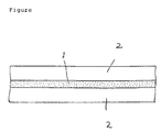
- FIG. 1 shows a cross-sectional view of the liquid crystal display device of the present invention.
- the liquid crystal display device has a composite film 1 which is present between two transparent electrodes 2.
- the transparent electrode 2 is, for example, an electrically conductive layer (for example, indium tin oxide (ITO) and SnO2) formed on a transparent substrate such as a glass or a film of plastic (for example, polyethylene terephthalate (PET) or polyethersulfone (PES)) by a vapor deposition method, a sputtering method, a coating method and the like.
- a transparent substrate such as a glass or a film of plastic (for example, polyethylene terephthalate (PET) or polyethersulfone (PES)) by a vapor deposition method, a sputtering method, a coating method and the like.
- PET polyethylene terephthalate
- PES polyethersulfone
- the composite film may contain various conventionally known two-tone pigments so as to use the display device as a color display device.
- the liquid crystal material may be a nematic liquid crystal, a smectic liquid crystal and a cholesteric liquid crystal.
- the nematic liquid crystal is not limited, but is preferably one which has a large anisotropy of the dielectric constant ⁇ , since excellent properties can be obtained.
- the liquid crystal material may contain a chiral component.
- the cross-linked material (a) has higher flexibility than a cross-linked material of the conventional resin, since the carboxyl group-containing acrylonitrile/butadiene copolymer has a flexible butadiene unit.
- the carboxyl group-containing acrylonitrile/butadiene copolymer can be prepared by using (meth)acrylic acid as a third monomer when acrylonitrile and butadiene are copolymerized.
- a molar ratio of acrylonitrile, butadiene and (meth)acrylic acid can be suitably selected.
- An amount of acrylonitrile is preferably from 1 to 40 % by mole, more preferably from 5 to 35 % by mole, most preferably about 28 % by mole based on the polymer.
- An amount of butadiene is preferably from 98 to 50 % by mole, more preferably from 83 to 57 % by mole, most preferably about 68 % by mole based on the polymer.
- An amount of (meth)acrylic acid is preferably from 1 to 10 % by mole, more preferably from 2 to 8 % by mole, most preferably about 4 % by mole based on the polymer.
- a molecular weight of the acrylonitrile/butadiene copolymer is preferably from 100,000 to 5,000,000.
- the liquid crystal display device having the composite film containing the polymer matrix made of the cross-linked material of the carboxyl group-containing acrylonitrile/butadiene copolymer according to the present invention can be prepared in substantially the same manner as in a conventional liquid crystal display device having a composite film containing a polymer matrix made of a thermoplastic resin.
- the composite film having the continuous pores of the three-dimensional network polymer matrix filled with the liquid crystal material is prepared by coating the coating liquid on the surface of one of transparent electrodes, which coating liquid comprises the liquid crystal material, the carboxyl group-containing acrylonitrile/butadiene copolymer and the oxazoline compound dissolved or dispersed in the solvent, and evaporating the solvent to separate the polymer phase from the liquid crystal material phase.
- the carboxyl group-containing acrylonitrile/butadiene copolymer carries out an addition reaction with the oxazoline compound simultaneously with the formation of the composite film by the phase separation. Therefore, the polymer matrix having the continuous pores finally consists of the cross-linked material which is an addition reaction product.
- the addition reaction is initiated by mixing the oxazoline compound with the copolymer in the coating liquid.
- the both components are mixed preferably immediately before coating the coating liquid on the surface of the transparent electrode so as to prevent the unhomogenous coating due to the premature addition reaction. It is recommendable to separately prepare the oxazoline compound and the coating liquid containing the liquid crystal material and the carboxyl group-containing acrylonitrile/butadiene copolymer dissolved or dispersed in the solvent and to mix the oxazoline compound with the coating liquid immediately before the coating.
- the temperature and time in steps of from the coating liquid preparation to the composite film formation are preferably controlled so that residual amount of the oxazoline compound is small.
- an amount of the functional COOH group is preferably larger than that of the functional oxazoline group.
- a molar ratio of the functional COOH group to the oxazoline group is preferably from 0.2:1 to 5:1.
- the solvent can be selected from various solvents depending on the kinds of the acrylonitrile/butadiene copolymer, the oxazoline compound and the liquid crystal material.
- composition ratio of components is not critical, and it can be selected from various ratios according to the method for coating the coating liquid on the transparent electrode, a thickness of composite film and the like.
- a weight ratio of the acrylonitrile/butadiene copolymer to the liquid crystal in the coating liquid is preferably from 3:97 to 80:20, more preferably from 5:95 to 50:50.
- the polyamide acid which is a raw material for the polyimide resin can be prepared by a polycondensation of an aromatic diacid anhydride with an aromatic diamine.
- the polyamic acid may be provided in the form of a varnish, a film, powder or the like, and can be dissolved in a solvent or processed in the same manner as in a thermoplastic resin.
- Specific examples of the polyamide acid are as follows: (n is from 1 to 2000, preferably from 1 to 100)
- the imidation of the polyamic acid can be chemically conducted by a dehydration ring formation reaction using a dehydrating agent and a catalyst. But, the polyamide acid as such may only be heated to a certain temperature to conduct the dehydration ring formation reaction so that an imidation is proceeded to prepare the polyimide resin.
- the solvent can be selected from various solvents depending on the kinds of the polyamic acid and the liquid crystal material.
- a weight ratio of the component is not limited, and it can be selected depending on the method for coating the coating liquid on the transparent electrode, the thickness of the formed composite film and the like.
- a weight ratio of polyamic acid to the liquid crystal in the coating liquid is preferably from 2:98 to 80:20, more preferably from 5:95 to 50:50.
- the method for coating the coating liquid on the transparent electrode may be a conventional method such as a bar coating method, a spin coating method, a spray coating method, a roller coating method, and a curtain coating method.
- the same electrically conductive transparent film as the above transparent film was positioned on the composite film to prepare a liquid crystal display device.
- the conventional liquid crystal display devices having a polymer matrix made of a thermoplastic resin in Comparative Examples 1 to 3 have a high applied voltage giving a saturated transmittance and poor response to an applied voltage. In addition, they have poor heat resistance since a contrast after the heat treatment is significantly decreased.
- a liquid crystal display device was prepared in the same as in Example 4 except that an amic acid (refractive index: 1.485) was used instead of the fluorinated polyamic acid, chloroform was used as the solvent, and the composite film was dried at 200°C for 5 minutes to conduct the 70 % imidation of the amic acid.
- an amic acid reffractive index: 1.485
- chloroform chloroform
- Polymethyl methacrylate (Delpet manufactured by Asahi Kasei Kogyo) and a liquid crystal material (E63 manufactured by Merck, Japan) in a weight ratio of 4:6 were dissolved in acetone as a solvent to prepare a coating liquid (dissolved substance concentration as whole: 15 % by weight).
- a liquid crystal display device was prepared in the same manner as in Comparative Example 4 except that polystyrene (Dic styrene manufactured by Dainippon Ink) was used instead of polymethyl methacrylate.
- polystyrene Di styrene manufactured by Dainippon Ink
- the liquid crystal display device was positioned in a spectrophotometer (UV-160 manufactured by Shimadzu). An AC sinusoidal voltage of 60 Hz was applied between the transparent electrodes to measure relationship between an applied voltage and a transmittance of light having a 600 nm wave length.
- the liquid crystal display devices of Examples 4 to 6 have so low applied voltage giving a saturated transmittance that they have good response to an applied voltage, and they have no low contrast after the heat treatment such that they have excellent heat resistance.
Landscapes
- Chemical & Material Sciences (AREA)
- Organic Chemistry (AREA)
- Crystallography & Structural Chemistry (AREA)
- Physics & Mathematics (AREA)
- Engineering & Computer Science (AREA)
- Materials Engineering (AREA)
- Nonlinear Science (AREA)
- Health & Medical Sciences (AREA)
- Chemical Kinetics & Catalysis (AREA)
- Medicinal Chemistry (AREA)
- Polymers & Plastics (AREA)
- Optics & Photonics (AREA)
- General Physics & Mathematics (AREA)
- Liquid Crystal (AREA)
Applications Claiming Priority (2)
| Application Number | Priority Date | Filing Date | Title |
|---|---|---|---|
| JP30228/91 | 1991-02-25 | ||
| JP3030228A JPH06337404A (ja) | 1991-02-25 | 1991-02-25 | 液晶表示素子およびその製造方法 |
Publications (3)
| Publication Number | Publication Date |
|---|---|
| EP0501409A2 EP0501409A2 (en) | 1992-09-02 |
| EP0501409A3 EP0501409A3 (en) | 1992-09-23 |
| EP0501409B1 true EP0501409B1 (en) | 1995-05-03 |
Family
ID=12297859
Family Applications (1)
| Application Number | Title | Priority Date | Filing Date |
|---|---|---|---|
| EP92103156A Expired - Lifetime EP0501409B1 (en) | 1991-02-25 | 1992-02-25 | Liquid crystal display device and preparation thereof |
Country Status (8)
| Country | Link |
|---|---|
| US (1) | US5403510A (Direct) |
| EP (1) | EP0501409B1 (Direct) |
| JP (1) | JPH06337404A (Direct) |
| KR (1) | KR960005471B1 (Direct) |
| AU (1) | AU656759B2 (Direct) |
| CA (1) | CA2061696A1 (Direct) |
| DE (1) | DE69202276T2 (Direct) |
| TW (1) | TW222714B (Direct) |
Cited By (1)
| Publication number | Priority date | Publication date | Assignee | Title |
|---|---|---|---|---|
| US7008675B2 (en) | 2000-04-05 | 2006-03-07 | California Institute Of Techology | Polymers for orientation and stability of liquid crystals |
Families Citing this family (10)
| Publication number | Priority date | Publication date | Assignee | Title |
|---|---|---|---|---|
| US5812227A (en) * | 1992-04-02 | 1998-09-22 | Canon Kabushiki Kaisha | Liquid crystal device, display apparatus using same and display method using same |
| FR2738831B1 (fr) * | 1995-09-19 | 1997-10-17 | Thomson Csf | Procede de fabrication de film de materiau a base de polymere |
| KR20020077439A (ko) * | 2000-12-14 | 2002-10-11 | 코닌클리케 필립스 일렉트로닉스 엔.브이. | 액정 디스플레이 라미네이트와 그 제조방법 |
| KR20030053567A (ko) * | 2001-12-22 | 2003-07-02 | 비오이 하이디스 테크놀로지 주식회사 | 고분자 분산형 액정 표시 소자의 제조 방법 |
| US7324180B2 (en) | 2002-09-06 | 2008-01-29 | Dai Nippon Printing Co., Ltd. | Laminated retardation optical element, process of producing the same, and liquid crystal display |
| JP2004191832A (ja) * | 2002-12-13 | 2004-07-08 | Dainippon Printing Co Ltd | 位相差素子、それを備えた表示素子及び位相差素子の製造方法 |
| US7832093B2 (en) * | 2007-06-11 | 2010-11-16 | Kent State University | Method of creating an electro-mechanical energy conversion device |
| CN102348779B (zh) | 2009-01-30 | 2015-07-29 | 加州理工学院 | 铁电液晶(flc)聚合物 |
| WO2012016130A2 (en) | 2010-07-30 | 2012-02-02 | California Institute Of Technology | Polymer-doped vertically-aligned nematic liquid crystals |
| KR20130063372A (ko) * | 2011-12-06 | 2013-06-14 | 삼성디스플레이 주식회사 | 3차원 영상 표시 장치 |
Family Cites Families (6)
| Publication number | Priority date | Publication date | Assignee | Title |
|---|---|---|---|---|
| US4182700A (en) * | 1976-07-20 | 1980-01-08 | Benton William J | Elastomeric polyurethane film containing dispersed discrete aggregates of liquid crystal and method of making the same |
| US4963402A (en) * | 1987-08-21 | 1990-10-16 | Minnesota Mining And Manufacturing Company | Films containing liquid crystalline polymers |
| CA1307576C (en) * | 1987-10-20 | 1992-09-15 | Yoshi Arai | Liquid crystal devices and process for producing the same |
| EP0352637B1 (en) * | 1988-07-26 | 1994-03-30 | Idemitsu Kosan Company Limited | Ferroelectric liquid crystal composition, liquid crystal optical device produced by using the ferroelectric liquid crystal composition, and method of producing the liquid crystal optical device |
| DE3919942A1 (de) * | 1989-06-19 | 1990-12-20 | Merck Patent Gmbh | Elektrooptisches fluessigkristallsystem |
| JPH0451021A (ja) * | 1990-06-18 | 1992-02-19 | Dainippon Ink & Chem Inc | 液昌デバイス及びその製造方法 |
-
1991
- 1991-02-25 JP JP3030228A patent/JPH06337404A/ja active Pending
-
1992
- 1992-02-24 CA CA002061696A patent/CA2061696A1/en not_active Abandoned
- 1992-02-24 TW TW081101351A patent/TW222714B/zh active
- 1992-02-25 EP EP92103156A patent/EP0501409B1/en not_active Expired - Lifetime
- 1992-02-25 KR KR1019920002909A patent/KR960005471B1/ko not_active Expired - Fee Related
- 1992-02-25 DE DE69202276T patent/DE69202276T2/de not_active Expired - Fee Related
- 1992-02-25 US US07/840,069 patent/US5403510A/en not_active Expired - Fee Related
- 1992-02-25 AU AU11194/92A patent/AU656759B2/en not_active Ceased
Cited By (2)
| Publication number | Priority date | Publication date | Assignee | Title |
|---|---|---|---|---|
| US7008675B2 (en) | 2000-04-05 | 2006-03-07 | California Institute Of Techology | Polymers for orientation and stability of liquid crystals |
| US7179509B2 (en) | 2000-04-05 | 2007-02-20 | California Institute Of Technology | Polymers for control of orientation and stability of liquid crystals |
Also Published As
| Publication number | Publication date |
|---|---|
| US5403510A (en) | 1995-04-04 |
| JPH06337404A (ja) | 1994-12-06 |
| AU1119492A (en) | 1992-08-27 |
| KR920016878A (ko) | 1992-09-25 |
| EP0501409A3 (en) | 1992-09-23 |
| EP0501409A2 (en) | 1992-09-02 |
| DE69202276D1 (de) | 1995-06-08 |
| TW222714B (Direct) | 1994-04-21 |
| DE69202276T2 (de) | 1995-10-19 |
| AU656759B2 (en) | 1995-02-16 |
| CA2061696A1 (en) | 1992-08-26 |
| KR960005471B1 (ko) | 1996-04-25 |
Similar Documents
| Publication | Publication Date | Title |
|---|---|---|
| EP0656927B1 (en) | Metallo organo liquid crystals in a polymer matrix | |
| EP0501409B1 (en) | Liquid crystal display device and preparation thereof | |
| TWI314900B (en) | Optical film, liquid crystal panel, and liquid crystal display apparatus | |
| KR102237291B1 (ko) | 조성물, 중합체, 액정 배향제, 액정 배향막, 위상차판, 편광판, 액정 배향막의 제조 방법 및 액정 소자 | |
| US4325610A (en) | Sealing agent for plastic liquid crystal display panels | |
| EP0277567A2 (en) | Liquid crystal element | |
| JP5513446B2 (ja) | 液晶配向剤、液晶配向膜および該液晶配向膜を有する液晶表示素子 | |
| EP0421240B1 (en) | Liquid crystal display element | |
| CN1111289C (zh) | 高反射率聚合物分散液晶光阀显示装置 | |
| US5461494A (en) | Ferroelectric liquid crystal device having colored film and protective film at non-pixel portions | |
| JP4003592B2 (ja) | 液晶配向剤および液晶表示素子 | |
| JP3532295B2 (ja) | 液晶光学素子の製造方法 | |
| JP3906033B2 (ja) | 液晶マイクロカプセルおよび液晶表示素子 | |
| JP2959635B2 (ja) | 液晶表示素子用補償板およびその製造方法 | |
| JP7121196B2 (ja) | リバースモードポリマー分散液晶表示装置 | |
| JPH0540254A (ja) | 液晶表示素子およびその製造方法 | |
| JPH0792452A (ja) | 液晶表示用高分子とそれを用いた液晶素子および液晶素子の製造方法 | |
| JPH04319911A (ja) | 液晶表示素子およびその製造方法 | |
| JPH05310851A (ja) | マトリクス用高分子化合物、液晶表示素子およびその製造方法 | |
| JPH06228240A (ja) | 液晶表示用高分子化合物、それを用いた液晶表示素子およびその製造方法 | |
| JP2560905B2 (ja) | 液晶表示装置 | |
| JP2766218B2 (ja) | 液晶光学素子の製造方法 | |
| JP2844880B2 (ja) | 液晶表示素子およびその製造方法 | |
| Kim et al. | Multi-domain alignment films of polystyrene/polyimide of liquid crystals | |
| JPH07175043A (ja) | 液晶素子及びその製法 |
Legal Events
| Date | Code | Title | Description |
|---|---|---|---|
| PUAI | Public reference made under article 153(3) epc to a published international application that has entered the european phase |
Free format text: ORIGINAL CODE: 0009012 |
|
| PUAL | Search report despatched |
Free format text: ORIGINAL CODE: 0009013 |
|
| AK | Designated contracting states |
Kind code of ref document: A2 Designated state(s): BE DE FR GB IT NL |
|
| AK | Designated contracting states |
Kind code of ref document: A3 Designated state(s): BE DE FR GB IT NL |
|
| 17P | Request for examination filed |
Effective date: 19930211 |
|
| 17Q | First examination report despatched |
Effective date: 19940701 |
|
| GRAA | (expected) grant |
Free format text: ORIGINAL CODE: 0009210 |
|
| AK | Designated contracting states |
Kind code of ref document: B1 Designated state(s): BE DE FR GB IT NL |
|
| ITF | It: translation for a ep patent filed | ||
| REF | Corresponds to: |
Ref document number: 69202276 Country of ref document: DE Date of ref document: 19950608 |
|
| ET | Fr: translation filed | ||
| ITPR | It: changes in ownership of a european patent |
Owner name: OFF.TA PUB.CO LIC.ZA USO NON ESCLUSIVO OFFERTA LIC |
|
| REG | Reference to a national code |
Ref country code: GB Ref legal event code: 746 Effective date: 19951115 |
|
| PLBE | No opposition filed within time limit |
Free format text: ORIGINAL CODE: 0009261 |
|
| REG | Reference to a national code |
Ref country code: FR Ref legal event code: D6 |
|
| STAA | Information on the status of an ep patent application or granted ep patent |
Free format text: STATUS: NO OPPOSITION FILED WITHIN TIME LIMIT |
|
| 26N | No opposition filed | ||
| PGFP | Annual fee paid to national office [announced via postgrant information from national office to epo] |
Ref country code: FR Payment date: 19980210 Year of fee payment: 7 |
|
| PGFP | Annual fee paid to national office [announced via postgrant information from national office to epo] |
Ref country code: GB Payment date: 19980216 Year of fee payment: 7 |
|
| PGFP | Annual fee paid to national office [announced via postgrant information from national office to epo] |
Ref country code: NL Payment date: 19980226 Year of fee payment: 7 |
|
| PGFP | Annual fee paid to national office [announced via postgrant information from national office to epo] |
Ref country code: DE Payment date: 19980306 Year of fee payment: 7 |
|
| PGFP | Annual fee paid to national office [announced via postgrant information from national office to epo] |
Ref country code: BE Payment date: 19980417 Year of fee payment: 7 |
|
| PG25 | Lapsed in a contracting state [announced via postgrant information from national office to epo] |
Ref country code: GB Free format text: LAPSE BECAUSE OF NON-PAYMENT OF DUE FEES Effective date: 19990225 |
|
| PG25 | Lapsed in a contracting state [announced via postgrant information from national office to epo] |
Ref country code: BE Free format text: LAPSE BECAUSE OF NON-PAYMENT OF DUE FEES Effective date: 19990228 |
|
| BERE | Be: lapsed |
Owner name: SUMITOMO ELECTRIC INDUSTRIES LTD Effective date: 19990228 |
|
| PG25 | Lapsed in a contracting state [announced via postgrant information from national office to epo] |
Ref country code: NL Free format text: LAPSE BECAUSE OF NON-PAYMENT OF DUE FEES Effective date: 19990901 |
|
| GBPC | Gb: european patent ceased through non-payment of renewal fee |
Effective date: 19990225 |
|
| PG25 | Lapsed in a contracting state [announced via postgrant information from national office to epo] |
Ref country code: FR Free format text: LAPSE BECAUSE OF NON-PAYMENT OF DUE FEES Effective date: 19991029 |
|
| PG25 | Lapsed in a contracting state [announced via postgrant information from national office to epo] |
Ref country code: DE Free format text: LAPSE BECAUSE OF NON-PAYMENT OF DUE FEES Effective date: 19991201 |
|
| REG | Reference to a national code |
Ref country code: FR Ref legal event code: ST |
|
| PG25 | Lapsed in a contracting state [announced via postgrant information from national office to epo] |
Ref country code: IT Free format text: LAPSE BECAUSE OF NON-PAYMENT OF DUE FEES Effective date: 20050225 |