EP0495519A2 - Vorrichtung und Verfahren zum Messen einer Probe - Google Patents
Vorrichtung und Verfahren zum Messen einer Probe Download PDFInfo
- Publication number
- EP0495519A2 EP0495519A2 EP92100764A EP92100764A EP0495519A2 EP 0495519 A2 EP0495519 A2 EP 0495519A2 EP 92100764 A EP92100764 A EP 92100764A EP 92100764 A EP92100764 A EP 92100764A EP 0495519 A2 EP0495519 A2 EP 0495519A2
- Authority
- EP
- European Patent Office
- Prior art keywords
- reaction solution
- carrier particles
- substance
- test specimen
- electrodes
- Prior art date
- Legal status (The legal status is an assumption and is not a legal conclusion. Google has not performed a legal analysis and makes no representation as to the accuracy of the status listed.)
- Granted
Links
Images


Classifications
-
- G—PHYSICS
- G01—MEASURING; TESTING
- G01N—INVESTIGATING OR ANALYSING MATERIALS BY DETERMINING THEIR CHEMICAL OR PHYSICAL PROPERTIES
- G01N33/00—Investigating or analysing materials by specific methods not covered by groups G01N1/00 - G01N31/00
- G01N33/48—Biological material, e.g. blood, urine; Haemocytometers
- G01N33/50—Chemical analysis of biological material, e.g. blood, urine; Testing involving biospecific ligand binding methods; Immunological testing
- G01N33/53—Immunoassay; Biospecific binding assay; Materials therefor
- G01N33/543—Immunoassay; Biospecific binding assay; Materials therefor with an insoluble carrier for immobilising immunochemicals
- G01N33/54366—Apparatus specially adapted for solid-phase testing
- G01N33/54373—Apparatus specially adapted for solid-phase testing involving physiochemical end-point determination, e.g. wave-guides, FETS, gratings
- G01N33/5438—Electrodes
-
- G—PHYSICS
- G01—MEASURING; TESTING
- G01N—INVESTIGATING OR ANALYSING MATERIALS BY DETERMINING THEIR CHEMICAL OR PHYSICAL PROPERTIES
- G01N21/00—Investigating or analysing materials by the use of optical means, i.e. using sub-millimetre waves, infrared, visible or ultraviolet light
- G01N21/75—Systems in which material is subjected to a chemical reaction, the progress or the result of the reaction being investigated
- G01N21/77—Systems in which material is subjected to a chemical reaction, the progress or the result of the reaction being investigated by observing the effect on a chemical indicator
- G01N21/82—Systems in which material is subjected to a chemical reaction, the progress or the result of the reaction being investigated by observing the effect on a chemical indicator producing a precipitate or turbidity
-
- G—PHYSICS
- G01—MEASURING; TESTING
- G01N—INVESTIGATING OR ANALYSING MATERIALS BY DETERMINING THEIR CHEMICAL OR PHYSICAL PROPERTIES
- G01N33/00—Investigating or analysing materials by specific methods not covered by groups G01N1/00 - G01N31/00
- G01N33/48—Biological material, e.g. blood, urine; Haemocytometers
- G01N33/50—Chemical analysis of biological material, e.g. blood, urine; Testing involving biospecific ligand binding methods; Immunological testing
- G01N33/53—Immunoassay; Biospecific binding assay; Materials therefor
- G01N33/5302—Apparatus specially adapted for immunological test procedures
- G01N33/5304—Reaction vessels, e.g. agglutination plates
-
- G—PHYSICS
- G01—MEASURING; TESTING
- G01N—INVESTIGATING OR ANALYSING MATERIALS BY DETERMINING THEIR CHEMICAL OR PHYSICAL PROPERTIES
- G01N33/00—Investigating or analysing materials by specific methods not covered by groups G01N1/00 - G01N31/00
- G01N33/48—Biological material, e.g. blood, urine; Haemocytometers
- G01N33/50—Chemical analysis of biological material, e.g. blood, urine; Testing involving biospecific ligand binding methods; Immunological testing
- G01N33/53—Immunoassay; Biospecific binding assay; Materials therefor
- G01N33/543—Immunoassay; Biospecific binding assay; Materials therefor with an insoluble carrier for immobilising immunochemicals
- G01N33/54313—Immunoassay; Biospecific binding assay; Materials therefor with an insoluble carrier for immobilising immunochemicals the carrier being characterised by its particulate form
-
- G—PHYSICS
- G01—MEASURING; TESTING
- G01N—INVESTIGATING OR ANALYSING MATERIALS BY DETERMINING THEIR CHEMICAL OR PHYSICAL PROPERTIES
- G01N21/00—Investigating or analysing materials by the use of optical means, i.e. using sub-millimetre waves, infrared, visible or ultraviolet light
- G01N21/17—Systems in which incident light is modified in accordance with the properties of the material investigated
- G01N21/59—Transmissivity
- G01N21/5907—Densitometers
- G01N2021/5915—Processing scan data in densitometry
- G01N2021/5953—Processing scan data in densitometry for detecting a spatial spectrum
-
- G—PHYSICS
- G01—MEASURING; TESTING
- G01N—INVESTIGATING OR ANALYSING MATERIALS BY DETERMINING THEIR CHEMICAL OR PHYSICAL PROPERTIES
- G01N21/00—Investigating or analysing materials by the use of optical means, i.e. using sub-millimetre waves, infrared, visible or ultraviolet light
- G01N21/17—Systems in which incident light is modified in accordance with the properties of the material investigated
- G01N21/59—Transmissivity
- G01N21/5907—Densitometers
- G01N2021/5957—Densitometers using an image detector type detector, e.g. CCD
Definitions
- the present invention relates to the field of measurement of a test specimen for detecting a substance in the test specimen qualitatively or quantitatively.
- immunoactive substance such as an antigen or an antibody which is specifically bound to a specified antibody or antigen
- a method for detecting in a test specimen so-called immunoactive substance such as an antigen or an antibody which is specifically bound to a specified antibody or antigen
- carrier particles latex particles, glass particles, ceramic particles, kaolin, carbon black, colloidal particles such as erythrocyte and other animal blood component, and the like
- the carrier particles are reacted with test specimen in a liquid medium, and the aggregating state of the carrier particles in the reaction solution is observed and verified with the naked eye, thereby detecting qualitatively the substance which is specifically bound to the sensitized substance.
- Fig. 1 is a diagram showing the structure of a first embodiment according to the present invention.
- a reference numeral 1 designates a sample plate for mounting the carrier particles which carry an immunoactive substance such as a monochronal antibody on opaque insoluble fine particles, and the reaction solution in which an objective substance to be detected is reacted in a liquid medium.
- a semiconductor laser light source 2 and collimator lens 3 are provided on the optical axis to face the sample plate 1 which is horizontally arranged.
- a lens 4 and a photoelectric element 5 such as the primary CCD are arranged on the optical axis behind the sample plate 1 to receive the light beam transmitted through the sample plate 1.
- the sample plate 1 is adjusted to match the front side focusing plane of the lens 4, and the photoelectric element 5 is adjusted to match the rear side focusing plane of the lens.
- Fig. 2 is a perspective view illustrating the sample plate 1.
- the sample plate 1 is produced in such a manner that a cross-finger type pattern of the comb-shaped opaque electrodes 1b and 1c is transferred by masking onto a substrate 1a made of glass or other transparent material by using photolithographing processing.
- the comb-shaped electrodes 1b and 1c are formed symmetrically by etching and chrome deposition, and these electrodes 1b and 1c are electrically isolated on the sample plate 1.
- the electrodes 1b and 1c are arranged so that the width between each of the comb-shaped electrodes 1b and 1c is 100 ⁇ m, the width of the electrode itself is 20 ⁇ m, the formed electrode interval is 40 ⁇ m, and the grating pitch (P) produced by the formed electrode is 60 ⁇ m.
- the size of the electrode area is greater than the illuminating laser beam diameter 10 mm ⁇ and its shape is square having each side of approximately 12 mm. Then, in the direction parallel to the comb-shaped electrodes 1b and 1c, the photoelectric element 5 is arranged with its longitudinal direction oriented therein.
- a controller 6 is provided for the system control.
- the output of this controller 6 is connected to the semiconductor laser light source 2 through a laser driver 7.
- the output of the controller 6 is directly connected to an amplifier 9 while it is also connected thereto through an alternating oscillator 8.
- the output from the amplifier 9 is connected to the respective comb-shaped electrodes 1b and 1c of the sample plate 1 so as to allow the alternating current voltage which varies periodically with the amplified voltage by the amplifier 9 to be applied to the comb-shaped electrodes 1b and 1c.
- the output of the controller 6 is connected to the photoelectric element 5 through the CCD driver 10.
- the output of the photoelectric element 5 is connected to the controller 6 through a waveform treatment circuit 11 and A/D converter 12.
- the output of the controller 6 is also connected to a ROM 17 and RAM 18 which are provided separately from ROM and RAM arranged in a display 13, keyboard 14, printer 15, disc memory 16, and controller 6.
- latex particles of 1.0 ⁇ m ⁇ are used as carrier particles to sensitize an immunoactive substance on the surface thereof, and an immunoactive substance is dispersed in a liquid medium having water as its main component to produce a reagent.
- those having ionic character of either cation or anion on the surface thereof are used. Under such state that this reaction solution being injected into the substrate 1a of the sample plate 1, the aggregating acceleration and measurement for a predetermined period of time are started by the operation of the keyboard 14.
- the ionic substances in the reaction solution such as the latex particles having the ionic character on its surface and other ionic substance such as ion in the solution, are vibrated by the alternating current voltage applied across the electrodes 1b and 1c, thus accelerating the aggregation accordingly.
- the aggregation of the reaction solution can be conditioned substantially constant. It may be possible to apply any voltage if the voltage can be varied as the time elapses. A pulse voltage may be applied instead of the alternating voltage for example.
- the light beam from the semiconductor laser light source 2 is irradiated on the sample plate 1 after having been converted into a parallel rays of light by the collimator lens 3, and the transmitted beam forms an image on the photoelectric element 5 by the function of the lens 4.
- a substantially periodic structure is formed by the opaque comb-shaped electrodes 1b and 1c, and the sample plate 1 is arranged on the front focusing plane of the lens 4 while the photoelectric element 5 is arranged on the rear side focusing plane thereof. It is therefore possible to obtain the spatial spectra of the sample plate 1 by the image formed on the photoelectric element 5.
- Figs. 3A to 3H illustrate the states of the comb-shaped electrodes 1b and 1c of the sample plate 1 and the aggregated particle groups as well as the spatial spectra obtained from the photoelectric element 5.
- Fig. 3A shows the state of the comb-shaped electrodes 1b and 1c without any reaction solution being injected. In this case, the substantially periodic structure is formed only by the comb-shaped electrodes 1b and 1c, and as shown in Fig. 3E, the spatial spectrum on the photoelectric element 5 has only the basic frequency component fo corresponding to its grating pitch d.
- the comb-shaped electrodes 1b and 1c present a rectangular amplitude grating, the higher harmonic wave component of the frequency fo is contained, though it is extremely slightly.
- the duty of the grating i.e., the width and interval of the electrodes, is not equal, thus allowing the higher harmonic wave component to produce a modulated spatial spectrum, but these effects are extremely small and negligible here. The description therefore is omitted.
- Fig. 3B illustrates the state where the aggregated particle group G is attracted to the comb-shaped electrode 1b by applying a negative voltage to the comb-shaped electrode 1b and a positive voltage to the comb-shaped electrode 1c after the acceleration of the aggregation by vibrating the reaction solution L for a predetermined period of time.
- a positive voltage is applied to the comb-shaped electrode 1b while a negative voltage is applied to the comb-shaped electrode 1c respectively, then the aggregation particle group G is attracted to the comb-shaped electrode 1c as shown in Fig. 3D.
- the phase of the diffracted light is different from the state shown in Fig. 3B, but the spatial spectrum becomes the same, thus enabling the frequency component fo/2 to appear as shown in Fig. 3H.
- the carrier particles can be vibrated electrically. Then, it is possible to obtain the spatial spectrum of the aggregation particle group G by controlling its position with the applied voltage to the comb-shaped electrodes 1b and 1c. Since the characteristics and amount of the immunoactive substance differentiate the size and amount of the aggregation particle group G to be created, it is possible to detect the presence of a desired immunoactive substance qualitatively or quantitatively by giving attention to the spatial spectrum, particularly of the level of the frequency components fo, fo/2, and 2 ⁇ fo.
- the comparisons with the reference data prepared in advance are executed, but when a calculation is made most simply, the data comparison can be executed using the varied portion of the spatial spectrum shown in Fig. 3E which can be of reference. If the spatial spectrum shown in Fig. 3E is subtracted from the spatial spectra measured in the states shown in Figs. 3B through 3D, then the contribution of the aggregation particle group G to the spatial spectrum can be obtained.
- the spatial spectrum on the photoelectric element 5 is substantially axisymmetric in the A - B direction with respect to the optical axis. It sufficies, therefore, if the photoelectric element 5 can detect a unidimensional spectrum distribution substantially on one side including the optical axis, and by reducing the numbers of the element, it becomes possible to read at higher speeds. Also, if the numbers of the element are small, the exposure time can be extended. Hence, the S/N ratio can be improved. Moreover, the resolution can be improved by making the size per element, i.e., the spatial sampling frequency of the spectrum distribution, smaller, thus, enabling the reduction of the fabrication cost.
- the comb-shaped electrodes 1b and 1c are of the opaque chrome pattern, other metals such as gold or aluminum can be used instead. Then these become an optically high contrast amplitude-type grating. Also, it is possible to form the comb-shaped electrodes 1b and 1c with a transparent material such as ITO. In such a case, the component produced by the contribution of the comb-shaped electrodes 1b and 1c in the spatial spectrum can be removed. In other words, the states of the spatial spectrum shown in Figs. 3B, 3C, and 30 become as shown in Figs. 4A, 4B, and 4C respectively. Consequently, only the frequency component of the aggregation particle group G can be detected, thus making it possible to improve the S/N ratio and the detection accuracy as well.
- the sample plate 1 since the refractive index of the glass substrate 1a of the sample plate 1 is approximately 1.5 and the refractive index of the ITO is approximately 1.9, the sample plate 1 becomes a phase-type grating including a phase difference proportional to the product of the difference between both the refractive indexes and the the thickness of the comb-shaped electrodes 1b and 1c when there is no reaction solution injected in the sample plate 1. Also, when the reaction solution is injected, the sample plate becomes a phase-type grating including a phase difference proportional to the product of the difference between the refractive indexes of both the reaction solution and the thickness of the comb-shaped electrodes 1b and 1c if there is any difference between the refractive indexes of the reaction solution and ITO.
- the NA of a Fourier transform lens is great, the intensity of the spectrum of the phase grating is small, and there is no problem although it depends on the degree of the modulation of the phase.
- Fig. 1 when the measurement starting signal is inputted into the controller 6 by the operation of the keyboard 14, data are inputted into the controller 6 either from the keyboard 14, disk memory 16, ROM 17 or RAM 18, the data including a test specimen which is the object of the detection, granular diameter of the carrier particles as information of the carrier particles used, the optical characteristics such as charging condition, refraction factor, and absorptance, a table carrying density, optimal alternating current frequency, voltage amplitude, application time, and the like, and the structure between the electrodes 1b and 1c, substrate material, resistance, capacitance, resonant frequency as information regarding the sample plate 1, and others. Then, the optimal measurement condition is determined from the data including these pieces of information.
- the optimal measurement condition is determined from the data including these pieces of information.
- the controller 6 controls the oscillator 8 and amplifier 9 to apply the alternating voltage between the comb-shaped electrodes 1b and 1c while controlling the laser driver 7 to provide an optimal quantity of the laser light and further the CCD driver 10 to adjust the exposure time of the photoelectric element 5.
- the distribution of the spatial spectrum of the grating image projected on the photoelectric element 5 is converted into the time-series electric signals by the photoelectric element 5 being controlled by the CCD driver 10, and subsequent to the correction performed by the waveform treatment circuit 11, such signals are inputted into the controller 6 through the A/D converter 12 to execute the qualitative and quantitative detection.
- the result thereof is output to the display 13, printer 15, disc memory 16, RAM 18, and the like.
- the sample hold, filtering, sensitivity correction of the photoelectric element 5 if required, dark output correction, shading correction of the optical system are executed for the output from the photoelectric element 5. It is preferable to make an arrangement so that the measurement can be repeated by modifying the quantity of the laser light from the semiconductor laser light source and the exposure time of the photoelectric element 5 as required after the data from the A/D converter 12 have been examined by the controller 6. Also, it may be possible to connect another D/A converter between the controller 6 and amplifier 9.
- FIG. 5 illustrates the principal structure of a second embodiment which is a modification of the above-mentioned embodiment.
- the same reference numerals as those appearing in Fig. 1 designate the same members.
- a divisional sensor 19 in which sensor cells 19a through 19d comprising four divisional PIN photodiodes are packaged is arranged at the rear side focusing position of the lens 4 instead of the photoelectric element 5 used in the first embodiment.
- the output of the divisional sensor 19 is connected to an amplifier 20, and the output of the amplifier 20 is connected to an A/D converter 21. Then, the output of the A/D converter 21 is connected to a controller 6. Also, the output of the controller 6 is connected to an amplifier 9 through a D/A converter 22.
- the other structure arrangement is the same as the first embodiment and the representations thereof are not shown in Fig. 5.
- the sensor 19a is arranged at a position to detect zeroth refraction light beam while each of the sensor cells 19b, 19c, and 19d is arranged at a position to detect each of the aforesaid frequency components 2 ⁇ f0, f0, and f0/2, thus making it possible to detect only the luminous intensity of each frequency component efficiently.
- the current proportional to the luminous intensity output from the divisional sensor 19 is inputted into the controller 6 for the data processing through the A/D converter 21 after its current/voltage conversion, voltage amplitude, filtering, and the like have been performed by the amplifier 20.
- the present embodiment while it is impossible to respond to the situation where the electrode pitches of the sample plate 1 are different or the spatial spectrum distribution varies due to the extremely different conditions of the aggregation, only the signal having the required frequency component can be detected efficiently. As a result, the structure of the apparatus and the signal processing become simpler. It may be possible to improve the selectivity of the detecting spectrum ranges by providing an aperture, pinhole, and the like in front of the divisional sensor 19 as required.
- the aggregating conditions are constantly maintained by applying to the comb-shaped electrodes an alternating voltage having a specific state for a predetermined time of period. Then, an optical detection is conducted in a static state where a direct current voltage is being applied for detecting the aggregated conditions in an equilibrium state or semiequilibrium state.
- a third embodiment according to the present invention will be described hereunder, in which a test specimen measurement is performed dynamically by grasping the changes in the transient response of the aggregation.
- the drawings used above are also used for reference.
- the sinusoidal wave output of an alternating oscillator 8 is applied to the sample plate 1 through the amplifier 9 by command from the controller 6 in order to accelerate aggregation.
- the sample plate 1 presents the state as shown in Fig. 3A while the spatial spectrum being obtained from the photoelectric element 5 presents the state as shown in Fig. 3E.
- the states shown respectively in Figs. 3B, 3C, 3D and 3B appear for each of the phases ⁇ /2, ⁇ , 3 ⁇ /2, and ⁇ of the sinusoidal wave.
- the peak value of the spatial spectrum (Figs. 3F, 3G, 3H, and 3F) is progressively increased at each phase of the sinusoidal wave.
- the output from the photoelectric element 5 is drawn in synchronism with each phases of the sinusoidal wave of the alternating oscillator 8 in the present embodiment, or the output of the photoelectric element 5 which is synchronized with the phase of the sinusoidal wave is drawn by causing the light source 2 to emit pulse light at a desirable phase to be drawn in synchronism with the sinusoidal wave. Then, by evaluating the data thus obtained, it is possible to measure the transient response of the aggregating reaction.
- the inclination or inflection point of the transient response curve to be obtained by tracing timewise, for example, the peak of the frequency 2f0 in Fig. 3G showing the state of the spatial spectrum corresponding to the phase 3 ⁇ /2 of the sinusoidal wave, or to implement the improvement of the measuring accuracy of the test specimen on the basis of the shortened period of time for the test specimen measurement and transient response characteristics by making a simple threshold evaluation.
- the present invention is not limited to these conditions.
- test specimens should desirably be separated, it is effective to evaluate the difference of the transient response characteristics.
- time-frequency responses against the voltage applied to the aggregation particle group G are different by the test specimens, it is possible to improve the measuring accuracy of the test specimen more by making the output of the alternating oscillator 8 repeated sweeping waveforms or making the plural frequencies overlapped alternating waveforms.
- the reaction solution mounted on the substrate can be vibrated by the alternating voltage applied to the comb-shaped electrodes to accelerate the aggregation.
- the aggregating conditions can be maintained invariably.
- the spatial spectrum created by the comb-shaped electrodes, on which reaction solution mounted is detected thereby to detect by its changes the presence of the immunoactive substance in the test specimen by qualitatively or quantitatively.
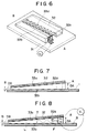
- Fig. 6 is a view showing the structure of a fourth embodiment according to the present invention.
- Fig. 7 is a vertically cross-sectional view in the direction A and B in Fig. 6.
- a wedge-shaped covering member 32 which is made of a transparent material with a concavity 32a arranged in the central inner side thereof, is closely provided, and a spatial portion is formed by the concavity 32a.
- a wedge-shaped covering member 32 which is made of a transparent material with a concavity 32a arranged in the central inner side thereof, is closely provided, and a spatial portion is formed by the concavity 32a.
- this concavity 32a is arranged so that the height of the space between the upper portion of the concavity 32a and the substrate 31 is gradually narrowed uniformly in the direction from A to B, and the vertical space DB at the end of the opening thereof is narrower than the diameter of the carrier particles to be used.
- the vertical space DA at the end of the opening in the A direction is wider than the vertical space DB by several times to approximately several hundred times so as to allow the aggregated particles to pass therethrough.
- comb-shaped electrodes 33a and 33b are formed respectively.
- these comb-shaped electrodes 33a and 33b are arranged to face each other with deviation as shown in Fig. 7.
- fluorescent carrier particles or colored carrier particles are prepared.
- an immunoactive substance is sensitized to these particles.
- the particles thus prepared are mixed with a reagent and test specimen dispersed in a liquid medium having water as it main component to produce a mixture.
- this mixture L is injected into the clearance between the substrate 32 and concavity 32a from the position A, the mixture L advances by surface tension in the direction B where the vertical space is getting narrower as shown in Fig. 8.
- the carrier particles F are given a force toward the direction Ff.
- the immunoactive substance has a polar group when it is in a liquid medium. Therefore, this substance is affected by a force from an electric field.
- the carrier particles F to which the immunoactive substance is sensitized are affected by a force from an electric field. However, it may be possible to given a polarity to the carrier particles F in advance.
- a time-changing voltage is applied to the comb-shaped electrodes 33a and 33b, a time-changing force Fd or Fu is given to the carrier particles F in response to the polarity of the electrode as shown in Fig. 8.
- the carrier particles F are immersed in the direction B with a locus represented by an arrow T.
- the immunoactive substance in the test specimen being given a force of the time-changing electric field, is immersed in the direction B with a waveform locus represented by an arrow T.
- this locus has different amplitude and frequency because the polarity or its intensity, mass and diameter thereof are different.
- the agitation of the carrier particles F and test specimen is accelerated, and further at the same time of the aggregation being accelerated, the carrier particles F and aggretated matter are immersed in the direction B where the clearance is getting narrower.
- the small diameter particles F can be carried further in the direction B, but the aggregated matter G is trapped on the way and cannot be carried any further depending on the size thereof.
- the diameter of the aggregated matter G which is determined by the numbers of the carrier particles F which constitute one aggregated matter G, and the numbers of the aggregated matter G trapped by a certain clearance have a correlation with the characteristics and numbers of the immunoactive substance contained in the reaction liquid L, i.e., the aggregating state of the aggregated matter G created by the reaction. Consequently, with the reaction solution L flown into such clearance, it becomes possible for an examiner to discriminate and recognize with the naked eye easily the quantity of the carrier particles F trapped by the clearance R which is equal to the diameter R of the single carrier particles F as well as the position where the aggregated matter G is trapped. Thus, the qualitative and quantitative detection of the immunoactive substance can be conducted.
- the calibration curve is prepared in advance by the reaction solution L which has been reacted on a measuring test specimen containing the know immunoactive substance, and the detection is conducted by making comparison with such a calibration curve.
- an opaque material for either one of the substrate 31 and cover member 32.
- a material having a desirable affinity with the liquid medium for the reaction solution L can be coated on the inner surface of the clearance. Then, a more desirable result of the measurement is obtainable.
- the coating material it is preferable to use a hydrophilic substance, interfacial active agent, methylcellulose, carboxy methylcellulose, polyvinyl alcohl, polyacrylamide, or other water-soluble polymer if the liquid medium is water.
- Fig. 10 is a view illustrating the structure of a fifth embodiment according to the present invention.
- a flat cover member 32 made of a transparent material with a concavity 32b arranged in the central inner side thereof is closely provided on the substrate 31 to form a clearance.
- This concavity 32b is arranged so that the height between the substrate 31 and concavity 32b is gradually shortened in four steps in the direction from A to B.
- the vertical space DB in the opening at the end portion in the B direction is smaller than the diameter of the carrier particles F while the vertical space DA in the opening at the end portion in the A direction is larger than the vertical space DB by several times to approximately several hundred times so as to allow the aggregated matter G to pass therethrough.
- flat electrodes 33c and 33d are formed on the side portions of the concavity 32b to face each other.
- the mixture L is injected from the position A, and when a time-changing voltage is applied to the electrodes 33c and 33d, a force Ff created by the surface tension and forces Fr and Fl are given by the time-changing polarities of the electrodes 33c and 33d to the carrier particles F and immunoactive substance in the test specimen as in the fourth embodiment.
- these particles and substance are caused to advance in the direction B with the locus represented by an arrow T so that the agitation and aggregation are accelerated.
- the aggregated matter G is trapped on the way, and at the same time the distribution corresponding to each aggregation state is formed in the direction of the aforesaid electrodes in accordance with the voltage applied to the electrodes 33c and 33d as in the cases of the first embodiment and second embodiment.
- the qualitative and moreover, quantitative detection of the immunoactive substance can be performed.
- Fig. 11 illustrates the structure of a sixth embodiment according to the present invention.
- a flat cover member 32 made of a transparent material with a concavity 32c arranged in the central inner side thereof is closely provided on the substrate 31 to form a clearance in the third embodiment.
- the vertical space of the clearance between the concavity 32c and substrate 31 is gradually narrowed uniformly in the direction from A to B, and from the position of the vertical space DB which is smaller than the diameter of the carrier particles F to be used, the width of the clearance is constant.
- the volume of the clearance SB of the vertical space DB is made substantially equal to the volume of the clearance SA which has a larger vertical space than the vertical space DB or greater than that.
- the vertical space DA of the opening at the end portion in the direction A is larger than the vertical space DB by several times to several hundred times so as to allow the aggregated matter G to pass therethrough.
- the flat electrodes 33e and 33f are provided respectively and a time-changing voltage is applied to them.
- the mixture L when the mixture L is injected into the clearance between the substrate 31 and cover member 32 from the position A, the mixture L is caused by the surface tension to be immersed in the direction B where the vertical space is getting narrower while being given the force of the time-changing electric fields of the electrodes 33a and 33b. Accordingly, as in the fourth embodiment, the agitation and aggregation are accelerated. Then, the carrier particles F and aggregated matter G are trapped at the positions matching the respective diameters thereof. Hence, only the mixture of the liquid medium and test specimen is allowed to be transferred to the clearance SB of the vertical space DB.
- this clearance SB As the volume of this clearance SB is large, the major portion of the mixture which is not needed for detection is flown into this clearance, making it possible to detect only the trapped carrier particles F and aggregated matter G in the clearance SA of the larger vertical space more easily, thereby to obtain desirable measurement results.
- the shape of the vertical space DB is arbitrary as far as it satisfies the voluminal condition, and a liquid absorption member may also be provided in the clearance SB. Furthermore, it may be possible to define the vertical space DB slightly larger than the diameter of the carrier particles F within a limit of as much as approximately two times. In this case, the non-aggregated matter, i.e., the carrier particles F, are not trapped and absorbed into the clearance SB. Then, it becomes clearer and easier to discriminate the aggregated from the non-aggregated, hence making it possible to obtain better measurement results.
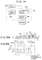
- Fig. 12 illustrates the structure of a seventh embodiment according to the present invention in order that the states of the reaction solution may be read automatically.
- Fig. 13 is a cross-sectional view showing the optical system.
- the sample plate 50 used here is the same as the one in the fourth embodiment shown in Fig. 6.
- a light source 51 is provided above the sample plate 50 to enable the fluorescent carrier particles to be excited through the band-pass filter and an image-formation optical system 52 comprising an image-formation lens, refraction factor contribution type lens, and the like is arranged below the sample plate 50.
- a light receiving optical system 53 is provided at a position where the image is formed.
- the light receiving optical system 53 there is provided in the inner portion of the frame 53a a CCD array 53b having photosensitive elements of 14 ⁇ m x 14 ⁇ m (size) per element, which are arranged uni- or two-dimensionally, for example.
- This CCD array 53b is protected by a glass protection plate 53c mounted on the frame 53a.
- the output of each photosensitive element of the CCD array 53b is connected to the signal treatment unit 55 through a cable 54.
- the output of the signal treatment unit 55 is connected to a monitor 56.
- the inner structure of the signal treatment unit 55 is as shown in Fig. 14, and the output of the CCD array 53b is connected to the CCD driver circuit 55a and arithmetical circuit 55b.
- the output of the CCD driver circuit 55a is connected to the arithmetical circuit 55b.
- the output of the arithmetical circuit 55b is connected to a display circuit 55c.
- the output of the display circuit 55c is connected to the monitor 56.
- An immunoactive substance such as a monochronal antibody is sensitized to the fluorescent carrier particles F emitting fluoresce.
- carrier particles F When such carrier particles F are mixed with a reagent and test specimen dispersed in a liquid medium having water as its main component, a reaction occurs. Then, the plural numbers of the immunoactive substance and carrier particles F form an aggregated matter G. After a sufficient reaction, this reaction solution L is injected into the clearance between the substrate 41 and concavity 42a from the position A as shown in Fig. 15A. Then, as in the case of the aforesaid fourth embodiment, the agitation of the carrier particles F and test specimen is accelerated.
- the carrier particles F and its aggregated matter are immersed in the direction B into the narrower clearance.
- the particles F which have a smaller diameter can be transferred deeply in the direction B, but the aggregated matter G is trapped on the way due to its diameter and cannot be transferred any further.
- the fluorescent image of the reaction solution L in the concavity 42a of the sample plate 10 is focused by the image-formation optical system 52 on the CCD array 53b of the light receiving optical system 53 and is converted photoelectrically by the CCD driver circuit 55a.
- the output voltage value of each photosensitive element is inputted into the arithmetical circuit 55b.
- Fig. 15B shows the output voltages of each of the photosensitive elements corresponding to the image of the separated state represented in Fig. 15A.
- a calibration curve is prepared in advance by the reaction solution L reacted to the measuring test specimen containing the known immunoactive substance, and the comparison is made therewith to make determination.
- the distribution of the maximal values of the output voltages h1, h2, h3, and h4 and the amplitudes d1, d2, d3, and d4 are compared with that of the calibration curve, or it may be possible to count simply the numbers of the photosensitive elements having the higher output voltage values than the threshold value Vs for comparison.
- the processing method thereof is not limitted to the abovementioned method.
- the results of the arithmetic processing are displayed on the monitor 56 through the display circuit 55c.
- the test specimen measuring apparatus set forth above is provided with a clearance which is gradually narrowed with uniformity or steps from a maximal space which is sufficiently larger than the diameter of the carrier particles to a minimal space which smaller than the diameter of the carrier particles and is of a simple structure that electrodes are formed on the planes of the clearance which face each other.
- a time-changing voltage is applied to the electrodes and a mixture is injected from the opening having the maximal space, the carrier particles and aggregated matter are agitated and aggregated by the electric field thus generated.
- the carrier particles, aggregated matter, liquid medium, and the like which are different in the sizes thereof are separated.
- the aggregating degree of the reaction solution can be discriminated and recognized clearly, and by comparing the calibration curve prepared in advance or the like means, it is possible to perform the qualitative or quantitative detection of the immunoactive substance in the test specimen highly precisely with a desirable producibility.
Applications Claiming Priority (6)
| Application Number | Priority Date | Filing Date | Title |
|---|---|---|---|
| JP1955191 | 1991-01-18 | ||
| JP19551/91 | 1991-01-18 | ||
| JP34915491A JP2652293B2 (ja) | 1991-12-06 | 1991-12-06 | 検体測定装置 |
| JP349154/91 | 1991-12-06 | ||
| JP20416/92 | 1992-01-08 | ||
| JP4020416A JP2691267B2 (ja) | 1991-01-18 | 1992-01-08 | 検体測定装置 |
Publications (3)
| Publication Number | Publication Date |
|---|---|
| EP0495519A2 true EP0495519A2 (de) | 1992-07-22 |
| EP0495519A3 EP0495519A3 (en) | 1993-01-13 |
| EP0495519B1 EP0495519B1 (de) | 1996-10-16 |
Family
ID=27282674
Family Applications (1)
| Application Number | Title | Priority Date | Filing Date |
|---|---|---|---|
| EP92100764A Expired - Lifetime EP0495519B1 (de) | 1991-01-18 | 1992-01-17 | Vorrichtung und Verfahren zum Messen einer Probe |
Country Status (3)
| Country | Link |
|---|---|
| US (1) | US5380490A (de) |
| EP (1) | EP0495519B1 (de) |
| DE (1) | DE69214471T2 (de) |
Cited By (2)
| Publication number | Priority date | Publication date | Assignee | Title |
|---|---|---|---|---|
| EP0767376A2 (de) * | 1995-10-06 | 1997-04-09 | Isao Karube | Verfahren zur Detektion oder zum Messen einer immunologisch reaktiven Substanz |
| WO1999027367A1 (de) * | 1997-11-21 | 1999-06-03 | Meinhard Knoll | Vorrichtung und verfahren zum nachweis von analyten |
Families Citing this family (8)
| Publication number | Priority date | Publication date | Assignee | Title |
|---|---|---|---|---|
| US5719033A (en) * | 1995-06-28 | 1998-02-17 | Motorola, Inc. | Thin film transistor bio/chemical sensor |
| JP4632400B2 (ja) * | 2003-12-16 | 2011-02-16 | キヤノン株式会社 | 細胞培養用基板、その製造方法、それを用いた細胞スクリーニング法 |
| EP1694812A4 (de) * | 2003-12-16 | 2008-11-12 | Canon Kk | Blatt zur übertragung biologisch aktiver substanzen, aus einer zellkulturplatte und dem blatt zur übertragung biologisch aktiver substanzen bestehender zellkultur-kit, herstellungsverfahren dafür und verfahren zum screening von zellkulturbedingungen unter verwendung davon |
| JP4515162B2 (ja) * | 2004-06-15 | 2010-07-28 | キヤノン株式会社 | Dnaインターカレート物質類の吸着用構造物 |
| JP4147235B2 (ja) * | 2004-09-27 | 2008-09-10 | キヤノン株式会社 | 吐出用液体、吐出方法、液滴化方法、液体吐出カートリッジ及び吐出装置 |
| US20060191884A1 (en) * | 2005-01-21 | 2006-08-31 | Johnson Shepard D | High-speed, precise, laser-based material processing method and system |
| JP4689340B2 (ja) * | 2005-05-02 | 2011-05-25 | キヤノン株式会社 | 吐出用液体医薬組成物 |
| US20110243850A1 (en) | 2008-12-25 | 2011-10-06 | Canon Kabushiki Kaisha | Probe for a biological specimen and labelling method and screening method using the probe |
Citations (7)
| Publication number | Priority date | Publication date | Assignee | Title |
|---|---|---|---|---|
| EP0079717A1 (de) * | 1981-11-02 | 1983-05-25 | Olympus Optical Co., Ltd. | Verfahren zur Beurteilung einer Agglutinationsreaktion und Reaktionsgefäss für dieses Verfahren |
| EP0117988A1 (de) * | 1983-02-03 | 1984-09-12 | Virgil B. Elings | Immunoassay |
| EP0170375A2 (de) * | 1984-06-13 | 1986-02-05 | Unilever Plc | Vorrichtungen zur Verwendung in chemischen Analyseverfahren |
| US4596695A (en) * | 1984-09-10 | 1986-06-24 | Cottingham Hugh V | Agglutinographic reaction chamber |
| EP0246846A2 (de) * | 1986-05-20 | 1987-11-25 | AMERSHAM INTERNATIONAL plc | Verfahren und Gerät zur Bestimmung einer Spezies in einer Probe |
| EP0261868A2 (de) * | 1986-09-25 | 1988-03-30 | AMERSHAM INTERNATIONAL plc | Verfahren zur Teilchenanalyse |
| EP0479231A1 (de) * | 1990-10-01 | 1992-04-08 | Canon Kabushiki Kaisha | Vorrichtung und Verfahren zur Messung einer Probe |
Family Cites Families (15)
| Publication number | Priority date | Publication date | Assignee | Title |
|---|---|---|---|---|
| BE758864A (fr) * | 1969-11-13 | 1971-04-16 | Miles Lab | Instrument de mesure de conductivite differentielle |
| US3714562A (en) * | 1971-04-23 | 1973-01-30 | Selco Mining Corp Ltd | Method and apparatus for the detection of selected components in fluids |
| JPS6145479Y2 (de) * | 1979-09-10 | 1986-12-20 | ||
| JPS576338A (en) * | 1980-06-12 | 1982-01-13 | Kyoto Daiichi Kagaku:Kk | Method and device for measuring degree of flocculation of finely divided particles quantitatively |
| JPS57175957A (en) * | 1981-04-24 | 1982-10-29 | Chugai Pharmaceut Co Ltd | Measuring method and device for antigen- antibody reaction |
| JPS5821141A (ja) * | 1981-07-30 | 1983-02-07 | Olympus Optical Co Ltd | 粒子凝集反応判定方法および判定容器 |
| US4447396A (en) * | 1982-01-04 | 1984-05-08 | Olympus Optical Co., Ltd. | System for discriminating a precipitation pattern of particles |
| US5141868A (en) * | 1984-06-13 | 1992-08-25 | Internationale Octrooi Maatschappij "Octropa" Bv | Device for use in chemical test procedures |
| NL8403091A (nl) * | 1984-10-11 | 1986-05-01 | Gen Electric | Thermoplastisch mengsel met polyfunctionele verbinding. |
| US5066372A (en) * | 1986-05-02 | 1991-11-19 | Ciba Corning Diagnostics Corp. | Unitary multiple electrode sensor |
| JPH063448B2 (ja) * | 1987-03-31 | 1994-01-12 | 日本光電工業株式会社 | 抗原抗体反応検出方法及びその装置 |
| JP2667867B2 (ja) * | 1988-03-30 | 1997-10-27 | 東亜医用電子株式会社 | 粒子解析装置 |
| JP2761385B2 (ja) * | 1988-04-08 | 1998-06-04 | 東亜医用電子株式会社 | 免疫凝集測定装置 |
| US5093268A (en) * | 1988-04-28 | 1992-03-03 | Igen, Inc. | Apparatus for conducting a plurality of simultaneous measurements of electrochemiluminescent phenomena |
| US4999582A (en) * | 1989-12-15 | 1991-03-12 | Boehringer Mannheim Corp. | Biosensor electrode excitation circuit |
-
1992
- 1992-01-16 US US07/821,049 patent/US5380490A/en not_active Expired - Lifetime
- 1992-01-17 EP EP92100764A patent/EP0495519B1/de not_active Expired - Lifetime
- 1992-01-17 DE DE69214471T patent/DE69214471T2/de not_active Expired - Fee Related
Patent Citations (7)
| Publication number | Priority date | Publication date | Assignee | Title |
|---|---|---|---|---|
| EP0079717A1 (de) * | 1981-11-02 | 1983-05-25 | Olympus Optical Co., Ltd. | Verfahren zur Beurteilung einer Agglutinationsreaktion und Reaktionsgefäss für dieses Verfahren |
| EP0117988A1 (de) * | 1983-02-03 | 1984-09-12 | Virgil B. Elings | Immunoassay |
| EP0170375A2 (de) * | 1984-06-13 | 1986-02-05 | Unilever Plc | Vorrichtungen zur Verwendung in chemischen Analyseverfahren |
| US4596695A (en) * | 1984-09-10 | 1986-06-24 | Cottingham Hugh V | Agglutinographic reaction chamber |
| EP0246846A2 (de) * | 1986-05-20 | 1987-11-25 | AMERSHAM INTERNATIONAL plc | Verfahren und Gerät zur Bestimmung einer Spezies in einer Probe |
| EP0261868A2 (de) * | 1986-09-25 | 1988-03-30 | AMERSHAM INTERNATIONAL plc | Verfahren zur Teilchenanalyse |
| EP0479231A1 (de) * | 1990-10-01 | 1992-04-08 | Canon Kabushiki Kaisha | Vorrichtung und Verfahren zur Messung einer Probe |
Cited By (4)
| Publication number | Priority date | Publication date | Assignee | Title |
|---|---|---|---|---|
| EP0767376A2 (de) * | 1995-10-06 | 1997-04-09 | Isao Karube | Verfahren zur Detektion oder zum Messen einer immunologisch reaktiven Substanz |
| EP0767376A3 (de) * | 1995-10-06 | 1998-08-12 | Isao Karube | Verfahren zur Detektion oder zum Messen einer immunologisch reaktiven Substanz |
| WO1999027367A1 (de) * | 1997-11-21 | 1999-06-03 | Meinhard Knoll | Vorrichtung und verfahren zum nachweis von analyten |
| US6548311B1 (en) | 1997-11-21 | 2003-04-15 | Meinhard Knoll | Device and method for detecting analytes |
Also Published As
| Publication number | Publication date |
|---|---|
| EP0495519B1 (de) | 1996-10-16 |
| DE69214471D1 (de) | 1996-11-21 |
| EP0495519A3 (en) | 1993-01-13 |
| DE69214471T2 (de) | 1997-04-24 |
| US5380490A (en) | 1995-01-10 |
Similar Documents
| Publication | Publication Date | Title |
|---|---|---|
| US5434667A (en) | Characterization of particles by modulated dynamic light scattering | |
| US5315375A (en) | Sensitive light detection system | |
| DE3546566C2 (de) | ||
| CN1040796C (zh) | 粒子分析装置 | |
| JP4201058B2 (ja) | 中間統計データに基づいて試料を特徴付けする方法 | |
| CN1041128C (zh) | 粒子分析装置 | |
| EP0495519B1 (de) | Vorrichtung und Verfahren zum Messen einer Probe | |
| JPS61501527A (ja) | 電気泳動光散乱を利用する方法及び装置 | |
| JPS61153546A (ja) | 粒子解析装置 | |
| US6613209B2 (en) | Toner characterization cell | |
| JPS6390740A (ja) | 粒子分析の方法及び装置 | |
| US8084002B2 (en) | Chemical sensing device | |
| JP2000131233A (ja) | 光学式インプロセス制御による比濁分析検出ユニット | |
| US6104490A (en) | Multiple pathlength sensor for determining small particle size distribution in high particle concentrations | |
| CN109073554B (zh) | 利用双光子激发荧光的生物亲和性测定方法 | |
| JPS61110033A (ja) | 凝集反応の測定装置 | |
| JP2675895B2 (ja) | 検体処理方法及び検体測定方法及び検体測定装置 | |
| JP2691267B2 (ja) | 検体測定装置 | |
| JP2652293B2 (ja) | 検体測定装置 | |
| JPH03154850A (ja) | 検体検査装置 | |
| JPH05288752A (ja) | 検体測定装置 | |
| JPH0545359A (ja) | 検体測定装置 | |
| JPH0621859B2 (ja) | 粒子測定装置 | |
| JPH03146848A (ja) | アライメント機構を備える検体測定装置 | |
| SU1455283A1 (ru) | Способ гранулометрического анализа дисперсных сред и устройство дл его осуществлени |
Legal Events
| Date | Code | Title | Description |
|---|---|---|---|
| PUAI | Public reference made under article 153(3) epc to a published international application that has entered the european phase |
Free format text: ORIGINAL CODE: 0009012 |
|
| AK | Designated contracting states |
Kind code of ref document: A2 Designated state(s): DE DK FR GB IT NL SE |
|
| PUAL | Search report despatched |
Free format text: ORIGINAL CODE: 0009013 |
|
| AK | Designated contracting states |
Kind code of ref document: A3 Designated state(s): DE DK FR GB IT NL SE |
|
| 17P | Request for examination filed |
Effective date: 19930525 |
|
| 17Q | First examination report despatched |
Effective date: 19951012 |
|
| GRAG | Despatch of communication of intention to grant |
Free format text: ORIGINAL CODE: EPIDOS AGRA |
|
| GRAH | Despatch of communication of intention to grant a patent |
Free format text: ORIGINAL CODE: EPIDOS IGRA |
|
| GRAH | Despatch of communication of intention to grant a patent |
Free format text: ORIGINAL CODE: EPIDOS IGRA |
|
| GRAA | (expected) grant |
Free format text: ORIGINAL CODE: 0009210 |
|
| AK | Designated contracting states |
Kind code of ref document: B1 Designated state(s): DE DK FR GB IT NL SE |
|
| PG25 | Lapsed in a contracting state [announced via postgrant information from national office to epo] |
Ref country code: IT Free format text: LAPSE BECAUSE OF FAILURE TO SUBMIT A TRANSLATION OF THE DESCRIPTION OR TO PAY THE FEE WITHIN THE PRE;WARNING: LAPSES OF ITALIAN PATENTS WITH EFFECTIVE DATE BEFORE 2007 MAY HAVE OCCURRED AT ANY TIME BEFORE 2007. THE CORRECT EFFECTIVE DATE MAY BE DIFFERENT FROM THE ONE RECORDED.SCRIBED TIME-LIMIT Effective date: 19961016 Ref country code: FR Effective date: 19961016 Ref country code: NL Free format text: LAPSE BECAUSE OF FAILURE TO SUBMIT A TRANSLATION OF THE DESCRIPTION OR TO PAY THE FEE WITHIN THE PRESCRIBED TIME-LIMIT Effective date: 19961016 Ref country code: DK Effective date: 19961016 |
|
| REF | Corresponds to: |
Ref document number: 69214471 Country of ref document: DE Date of ref document: 19961121 |
|
| PG25 | Lapsed in a contracting state [announced via postgrant information from national office to epo] |
Ref country code: SE Effective date: 19970116 |
|
| NLV1 | Nl: lapsed or annulled due to failure to fulfill the requirements of art. 29p and 29m of the patents act | ||
| EN | Fr: translation not filed | ||
| EN | Fr: translation not filed |
Free format text: CORRECTIONS |
|
| PLBE | No opposition filed within time limit |
Free format text: ORIGINAL CODE: 0009261 |
|
| STAA | Information on the status of an ep patent application or granted ep patent |
Free format text: STATUS: NO OPPOSITION FILED WITHIN TIME LIMIT |
|
| 26N | No opposition filed | ||
| REG | Reference to a national code |
Ref country code: GB Ref legal event code: IF02 |
|
| PGFP | Annual fee paid to national office [announced via postgrant information from national office to epo] |
Ref country code: GB Payment date: 20050112 Year of fee payment: 14 |
|
| PGFP | Annual fee paid to national office [announced via postgrant information from national office to epo] |
Ref country code: DE Payment date: 20050113 Year of fee payment: 14 |
|
| PG25 | Lapsed in a contracting state [announced via postgrant information from national office to epo] |
Ref country code: GB Free format text: LAPSE BECAUSE OF NON-PAYMENT OF DUE FEES Effective date: 20060117 |
|
| PG25 | Lapsed in a contracting state [announced via postgrant information from national office to epo] |
Ref country code: DE Free format text: LAPSE BECAUSE OF NON-PAYMENT OF DUE FEES Effective date: 20060801 |
|
| GBPC | Gb: european patent ceased through non-payment of renewal fee |
Effective date: 20060117 |