EP0246846A2 - Verfahren und Gerät zur Bestimmung einer Spezies in einer Probe - Google Patents
Verfahren und Gerät zur Bestimmung einer Spezies in einer Probe Download PDFInfo
- Publication number
- EP0246846A2 EP0246846A2 EP87304391A EP87304391A EP0246846A2 EP 0246846 A2 EP0246846 A2 EP 0246846A2 EP 87304391 A EP87304391 A EP 87304391A EP 87304391 A EP87304391 A EP 87304391A EP 0246846 A2 EP0246846 A2 EP 0246846A2
- Authority
- EP
- European Patent Office
- Prior art keywords
- piezoelectric material
- thin film
- radiation
- sample
- diffracted
- Prior art date
- Legal status (The legal status is an assumption and is not a legal conclusion. Google has not performed a legal analysis and makes no representation as to the accuracy of the status listed.)
- Granted
Links
Images
Classifications
-
- G—PHYSICS
- G01—MEASURING; TESTING
- G01N—INVESTIGATING OR ANALYSING MATERIALS BY DETERMINING THEIR CHEMICAL OR PHYSICAL PROPERTIES
- G01N21/00—Investigating or analysing materials by the use of optical means, i.e. using sub-millimetre waves, infrared, visible or ultraviolet light
- G01N21/17—Systems in which incident light is modified in accordance with the properties of the material investigated
- G01N21/55—Specular reflectivity
- G01N21/552—Attenuated total reflection
- G01N21/553—Attenuated total reflection and using surface plasmons
-
- G—PHYSICS
- G01—MEASURING; TESTING
- G01N—INVESTIGATING OR ANALYSING MATERIALS BY DETERMINING THEIR CHEMICAL OR PHYSICAL PROPERTIES
- G01N21/00—Investigating or analysing materials by the use of optical means, i.e. using sub-millimetre waves, infrared, visible or ultraviolet light
- G01N21/75—Systems in which material is subjected to a chemical reaction, the progress or the result of the reaction being investigated
- G01N21/77—Systems in which material is subjected to a chemical reaction, the progress or the result of the reaction being investigated by observing the effect on a chemical indicator
- G01N21/7703—Systems in which material is subjected to a chemical reaction, the progress or the result of the reaction being investigated by observing the effect on a chemical indicator using reagent-clad optical fibres or optical waveguides
- G01N21/774—Systems in which material is subjected to a chemical reaction, the progress or the result of the reaction being investigated by observing the effect on a chemical indicator using reagent-clad optical fibres or optical waveguides the reagent being on a grating or periodic structure
-
- G—PHYSICS
- G01—MEASURING; TESTING
- G01N—INVESTIGATING OR ANALYSING MATERIALS BY DETERMINING THEIR CHEMICAL OR PHYSICAL PROPERTIES
- G01N29/00—Investigating or analysing materials by the use of ultrasonic, sonic or infrasonic waves; Visualisation of the interior of objects by transmitting ultrasonic or sonic waves through the object
- G01N29/02—Analysing fluids
- G01N29/022—Fluid sensors based on microsensors, e.g. quartz crystal-microbalance [QCM], surface acoustic wave [SAW] devices, tuning forks, cantilevers, flexural plate wave [FPW] devices
-
- G—PHYSICS
- G01—MEASURING; TESTING
- G01N—INVESTIGATING OR ANALYSING MATERIALS BY DETERMINING THEIR CHEMICAL OR PHYSICAL PROPERTIES
- G01N33/00—Investigating or analysing materials by specific methods not covered by groups G01N1/00 - G01N31/00
- G01N33/48—Biological material, e.g. blood, urine; Haemocytometers
- G01N33/50—Chemical analysis of biological material, e.g. blood, urine; Testing involving biospecific ligand binding methods; Immunological testing
- G01N33/53—Immunoassay; Biospecific binding assay; Materials therefor
- G01N33/543—Immunoassay; Biospecific binding assay; Materials therefor with an insoluble carrier for immobilising immunochemicals
- G01N33/54366—Apparatus specially adapted for solid-phase testing
- G01N33/54373—Apparatus specially adapted for solid-phase testing involving physiochemical end-point determination, e.g. wave-guides, FETS, gratings
-
- G—PHYSICS
- G01—MEASURING; TESTING
- G01N—INVESTIGATING OR ANALYSING MATERIALS BY DETERMINING THEIR CHEMICAL OR PHYSICAL PROPERTIES
- G01N21/00—Investigating or analysing materials by the use of optical means, i.e. using sub-millimetre waves, infrared, visible or ultraviolet light
- G01N21/17—Systems in which incident light is modified in accordance with the properties of the material investigated
- G01N21/1717—Systems in which incident light is modified in accordance with the properties of the material investigated with a modulation of one or more physical properties of the sample during the optical investigation, e.g. electro-reflectance
- G01N2021/1729—Piezomodulation
-
- G—PHYSICS
- G01—MEASURING; TESTING
- G01N—INVESTIGATING OR ANALYSING MATERIALS BY DETERMINING THEIR CHEMICAL OR PHYSICAL PROPERTIES
- G01N21/00—Investigating or analysing materials by the use of optical means, i.e. using sub-millimetre waves, infrared, visible or ultraviolet light
- G01N21/17—Systems in which incident light is modified in accordance with the properties of the material investigated
- G01N21/21—Polarisation-affecting properties
-
- G—PHYSICS
- G01—MEASURING; TESTING
- G01N—INVESTIGATING OR ANALYSING MATERIALS BY DETERMINING THEIR CHEMICAL OR PHYSICAL PROPERTIES
- G01N21/00—Investigating or analysing materials by the use of optical means, i.e. using sub-millimetre waves, infrared, visible or ultraviolet light
- G01N21/17—Systems in which incident light is modified in accordance with the properties of the material investigated
- G01N21/47—Scattering, i.e. diffuse reflection
- G01N21/4788—Diffraction
-
- G—PHYSICS
- G01—MEASURING; TESTING
- G01N—INVESTIGATING OR ANALYSING MATERIALS BY DETERMINING THEIR CHEMICAL OR PHYSICAL PROPERTIES
- G01N2291/00—Indexing codes associated with group G01N29/00
- G01N2291/02—Indexing codes associated with the analysed material
- G01N2291/024—Mixtures
- G01N2291/02466—Biological material, e.g. blood
-
- G—PHYSICS
- G01—MEASURING; TESTING
- G01N—INVESTIGATING OR ANALYSING MATERIALS BY DETERMINING THEIR CHEMICAL OR PHYSICAL PROPERTIES
- G01N2291/00—Indexing codes associated with group G01N29/00
- G01N2291/04—Wave modes and trajectories
- G01N2291/042—Wave modes
- G01N2291/0423—Surface waves, e.g. Rayleigh waves, Love waves
-
- G—PHYSICS
- G01—MEASURING; TESTING
- G01N—INVESTIGATING OR ANALYSING MATERIALS BY DETERMINING THEIR CHEMICAL OR PHYSICAL PROPERTIES
- G01N2291/00—Indexing codes associated with group G01N29/00
- G01N2291/04—Wave modes and trajectories
- G01N2291/042—Wave modes
- G01N2291/0426—Bulk waves, e.g. quartz crystal microbalance, torsional waves
-
- Y—GENERAL TAGGING OF NEW TECHNOLOGICAL DEVELOPMENTS; GENERAL TAGGING OF CROSS-SECTIONAL TECHNOLOGIES SPANNING OVER SEVERAL SECTIONS OF THE IPC; TECHNICAL SUBJECTS COVERED BY FORMER USPC CROSS-REFERENCE ART COLLECTIONS [XRACs] AND DIGESTS
- Y10—TECHNICAL SUBJECTS COVERED BY FORMER USPC
- Y10S—TECHNICAL SUBJECTS COVERED BY FORMER USPC CROSS-REFERENCE ART COLLECTIONS [XRACs] AND DIGESTS
- Y10S359/00—Optical: systems and elements
- Y10S359/90—Methods
-
- Y—GENERAL TAGGING OF NEW TECHNOLOGICAL DEVELOPMENTS; GENERAL TAGGING OF CROSS-SECTIONAL TECHNOLOGIES SPANNING OVER SEVERAL SECTIONS OF THE IPC; TECHNICAL SUBJECTS COVERED BY FORMER USPC CROSS-REFERENCE ART COLLECTIONS [XRACs] AND DIGESTS
- Y10—TECHNICAL SUBJECTS COVERED BY FORMER USPC
- Y10S—TECHNICAL SUBJECTS COVERED BY FORMER USPC CROSS-REFERENCE ART COLLECTIONS [XRACs] AND DIGESTS
- Y10S436/00—Chemistry: analytical and immunological testing
- Y10S436/805—Optical property
-
- Y—GENERAL TAGGING OF NEW TECHNOLOGICAL DEVELOPMENTS; GENERAL TAGGING OF CROSS-SECTIONAL TECHNOLOGIES SPANNING OVER SEVERAL SECTIONS OF THE IPC; TECHNICAL SUBJECTS COVERED BY FORMER USPC CROSS-REFERENCE ART COLLECTIONS [XRACs] AND DIGESTS
- Y10—TECHNICAL SUBJECTS COVERED BY FORMER USPC
- Y10S—TECHNICAL SUBJECTS COVERED BY FORMER USPC CROSS-REFERENCE ART COLLECTIONS [XRACs] AND DIGESTS
- Y10S436/00—Chemistry: analytical and immunological testing
- Y10S436/806—Electrical property or magnetic property
-
- Y—GENERAL TAGGING OF NEW TECHNOLOGICAL DEVELOPMENTS; GENERAL TAGGING OF CROSS-SECTIONAL TECHNOLOGIES SPANNING OVER SEVERAL SECTIONS OF THE IPC; TECHNICAL SUBJECTS COVERED BY FORMER USPC CROSS-REFERENCE ART COLLECTIONS [XRACs] AND DIGESTS
- Y10—TECHNICAL SUBJECTS COVERED BY FORMER USPC
- Y10S—TECHNICAL SUBJECTS COVERED BY FORMER USPC CROSS-REFERENCE ART COLLECTIONS [XRACs] AND DIGESTS
- Y10S436/00—Chemistry: analytical and immunological testing
- Y10S436/807—Apparatus included in process claim, e.g. physical support structures
Definitions
- This invention relates to a method of assaying a species in a liquid sample, generally a biological fluid, and to apparatus for use with such method.
- this "optically active" surface is a grating.
- a beam of suitably polarised light incident on the grating will give rise to diffraction or reflection properties which are dictated by the manner in which the sample reacts with the applied thin film of material.
- the angle of incidence of the beam may be a right angle, or may be variable, resulting in a reflectivity dip at a particular angle.
- the present invention seeks to improve on the sensitivity and versatility of this technique by providing that the aforsaid thin film of material is applied to the surface of a slab of piezoelectric material which latter is thence energising by means of electrical energy applied to a suitable electrode or electrodes. Vibrations within the piezoelectric material are coupled into the thin film which then exhibits the properties of a grating. Polarised light incident on the coated surface of the piezoelectric material can be detected after diffraction using a photodetector or similar, or alternatively the energy in the form of a plasmon wave, coupled into the piezoelectric material at the aformentioned dip at particular angles of incidence, may be detected.
- the invention also provides an apparatus for use with such method.
- Piezoelectric materials may be excited in such a way as to produce primarily surface waves or primarily bulk waves.
- the waves may travel continuously through the material or may form a stationary standing wave pattern. It is believed that the use of surface-wave excitation will be of particular application in the present invention.
- Devices which use such excitation known as surface acoustic wave (SAW) devices, comprise one or more transducers formed on the surface of a slab of a suitablerpiezoelectric material.
- An ac signal applied to one of the transducers causes an acoustic wave to be launched from that transducer which wave propagates along the surface of the piezoelectric material to a distant transducer or transducers where it may be reconverted into an ac signal.
- the properties of the SAW device determine the frequency of the waves which can propagate along the surface and the device thus acts electrically as an effective bandpass filter.
- the slight delay which occurs as the wave travels from one transducer to the other can be utilised in applications requiring a delay line.
- the wave whether travelling or standing, produces alternate areas of compression and rarefaction of the atoms of the material.
- a surface-wave device as distinct from a bulk-wave device, the wave propagates more slowly because the atoms at the surface are less firmly anchored than those within the material.
- Suitable piezoelectric materials include lithium niobate and polyvinylidene fluoride.
- the former of these has a number of attractive properties which make it particularly suitable in this application. It is a stand-alone substrate, is resistant to water and most acids, is optically transparent within the wavelength range 450 to 5000 nm, has a high melting point (1260 0 C) and Curie temperature (1210 0 C), a refractive index greater than 2.15 and is mechanically robust.
- SAW devices Being a common component of SAW devices, it is available in quantity in single crystal form and there is considerable expertise available in the deposition of electrodes onto it and the modification of its structure by diffused metals.
- Polyvinylidene fluoride is a piezoelectric polymer, is stable in aqueous environments up to 120°C with a broad band response (up to 10 GHz), but with an acoustic impedance only 2-3 times that of water. This latter is a disadvantage compared with ceramic or lithium niobate, whose acoustic impedance is about 16 times that of water, where decoupling from serum or other aqueous solutions is required.
- piezoelectric materials may have an advantage if the device is to be fabricated by deposition on a substrate, for example by sputtering, CVD processes etc. These could be zinc oxide or tantalum pentoxide, for example.
- the radiation incident on the surface of the piezoelectric material is electromagnetic radiation and is preferably in the visible region.
- the radiation interacts at the surface of the piezoelectric material so as to be diffracted and the diffracted light may be detected by a photodetector such as a strip imager, photodiode or charge-coupled device (CCD). Since the transparency of the sample (e.g. serum) is likely to be less than that of the piezoelectric material it may well be preferable to project the light from beneath (i.e. through the piezoelectric material), rather than from above and through the sample.
- a photodetector such as a strip imager, photodiode or charge-coupled device (CCD). Since the transparency of the sample (e.g. serum) is likely to be less than that of the piezoelectric material it may well be preferable to project the light from beneath (i.e. through the piezoelectric material), rather than from above and through the sample.
- the absorption of the light in diffracting through the device is a function of the properties of the coating applied to the surface of the piezoelectric material and is thus representative of the status of the reaction between the film and a sample applied thereto.
- the maximum absorption dip occurs at particular angles of incidence and this in itself is dictated by the coating properties.
- the properties of the coating can be studied either by keeping the angle of incidence steady, and observing the change in absorption which occurs as the reaction between the applied film and the sample takes place, or by "tuning" the angle of incidence for a dip as the reaction progresses or both.
- tuning can be carried out automatically using feedback techniques. Tuning can also be effected by varying the frequency of the excitation signal applied to the piezoelectric material. For example, one possible method using an SAW device is to tune for dip before the sample is added, then tune the SAW drive frequency to follow the dip as the reaction progresses. As before this can be achieved automatically using feedback techniques.
- the tuning for a dip is likely to be the most sensitive method. It is now known that the dip results from the coupling into the material of the grating - in this case the thin film of material coating the surface of the piezoelectric material - of energy which travels close to the surface of the material in the form of a surface plasmon polariton.
- the plasmon wave is associated with an evanescent wave which travels with the plasmon wave above the surface and indeed maintains the plasmon wave.
- the energy in the plasmon wave can be extracted from the material at a discontinuity, such as an edge, or further diffraction grating, and can be detected using suitable detectors.
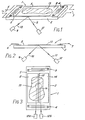
- the apparatus comprises an SAW device 1 comprising a slab 2 of piezoelectric material such as a crystal of lithium niobate.
- An input transducer 3 and an output transducer 4 are formed on the top surface 5 of the slab 2.
- Each transducer is formed from two sets of interleaved fingers of metallisation on the surface 5 and respective connections from the two sets of fingers are brought out to form input terminals 6 and output terminals 7.
- a source, not shown, of RF energy is applied to the input terminals 6 and may be picked up at the output terminals 7 by a suitable detector (also not shown).
- an RF signal applied to the input terminals generates at the input transducer a surface acoustic wave which travels across the surface creating compressions and rarefactions as the waves pass a particular point on the surface or a pattern of stationary compressions and rarefactions if a standing wave is set up.
- the attenuation of the wave in passing across the surface can be measured at the output terminals and indeed this measurement can itself act as a means for analysing the sample since the attenuation is dependent upon the nature of the surface and in particular the characteristics of any reaction which takes place on it.
- the material of the layer 8 and the species should form a specific binding pair, the nature of which is not critical.
- the species is an antigen or a hapten
- the material is preferably its associated antibody.
- the sample may conveniently be of a biological fluid, such as serum or plasma.
- a light source 9 generates a collimated beam 10 of suitably polarised light which is incident on the surface 5 from beneath the slab 2.
- Zero order diffracted light 11 is collected by a photodetector 12 which may take several forms, depending upon the circumstances: examples include a photo diode or photo-diode array, charge-coupled devices, a strip imager or a dynamic RAM imaging chip.
- the order of the light collected has no particular significance except that, having made the choice, consistency should be maintained.
- the light is incident from beneath the slab, this being to avoid possible attenuation in the sample; however there is no reason why light should not be incident from above and, in some circumstances, this may be preferred.
- the incident light could be pulsed in order to provide better discrimination over ambient light.
- This information can be used to assess the nature of the change in the surface properties, and in particular the concentration of antigen within the sample, as the antibody layer 8 changes on reaction with the analyte. It may be preferable to continuously monitor the level of light received at the photodetector during the test, rather than relying solely on discrete measurements taken at the beginning and end of the reaction. The manner in which the received light changes can give useful information.
- a more sensitive measure can be achieved by searching for the null in the diffracted light level, this occurring at particular angles of incidence and/or SAW device drive frequency. To do this, the null is found immediately after addition of the sample 13, either by moving the light source 9 to alter the angle of incidence, or by altering the drive frequency. Then, after waiting a predetermined time for the reaction to take place, the null can be re-found, using the same method, and the change noted. As before the change is an indication of the nature of the reaction that has taken place. Continuous monitoring can also be achieved with this method by arranging that the light source 9 is moved or drive frequency changed automatically, under feedback control, to track the null.
- FIG 3 two thin layers are laid down on the surface 5 of the piezoelectric crystal.
- the first of these, referenced 8 as before, contains antibodies to the expected antigen within the sample.
- the second, referenced 14, is identical with the first except that it is a non-specific coating.
- a narrow dividing line 15 separates the two areas 8 and 14, and the light from source 9 (not shown in Figure 3) is incident as a spot shown dotted under reference 16 about 3 mm in diameter and straddling the two areas.
- Light diffracted as a result of interference in the two areas is collected by separate photodetectors 12a (for area 8) and 12b (for area 14) which may each take any of the alternative forms of the photodetector 12 of Figures I and 2.
- the sample 13 is applied across both areas in the manner shown so that the reaction over the area 8 can be compared to the reaction over the area 14, and any compensations made.
- a similar technique to that shown in Figure 3 can be used where a sample is to be tested for a number of different antigens. To achieve this, a number of separate areas 8 of antibody can be applied to surface 5, each being specific to a different antigen.
- the spot 16 of incident light is arranged to cover at least a portion of each region, as well (preferably) as a non-specific control region, to provide for simultaneous testing of a number of antigens within a sample.
- One way of arranging such separate areas would be by way of a number of narrow strips arranged side by side on surface 5, each strip being an antibody specific to a particular expected antigen within the sample.
Landscapes
- Health & Medical Sciences (AREA)
- Immunology (AREA)
- Life Sciences & Earth Sciences (AREA)
- Chemical & Material Sciences (AREA)
- Physics & Mathematics (AREA)
- Pathology (AREA)
- Engineering & Computer Science (AREA)
- Analytical Chemistry (AREA)
- Biochemistry (AREA)
- General Health & Medical Sciences (AREA)
- General Physics & Mathematics (AREA)
- Biomedical Technology (AREA)
- Hematology (AREA)
- Urology & Nephrology (AREA)
- Molecular Biology (AREA)
- Microbiology (AREA)
- Cell Biology (AREA)
- Biotechnology (AREA)
- Chemical Kinetics & Catalysis (AREA)
- Plasma & Fusion (AREA)
- Acoustics & Sound (AREA)
- Food Science & Technology (AREA)
- Medicinal Chemistry (AREA)
- Investigating Or Analysing Materials By Optical Means (AREA)
- Analysing Materials By The Use Of Radiation (AREA)
Applications Claiming Priority (2)
| Application Number | Priority Date | Filing Date | Title |
|---|---|---|---|
| GB868612221A GB8612221D0 (en) | 1986-05-20 | 1986-05-20 | Assaying species in sample |
| GB8612221 | 1986-05-20 |
Publications (3)
| Publication Number | Publication Date |
|---|---|
| EP0246846A2 true EP0246846A2 (de) | 1987-11-25 |
| EP0246846A3 EP0246846A3 (en) | 1988-10-12 |
| EP0246846B1 EP0246846B1 (de) | 1991-08-14 |
Family
ID=10598119
Family Applications (1)
| Application Number | Title | Priority Date | Filing Date |
|---|---|---|---|
| EP87304391A Expired EP0246846B1 (de) | 1986-05-20 | 1987-05-18 | Verfahren und Gerät zur Bestimmung einer Spezies in einer Probe |
Country Status (5)
| Country | Link |
|---|---|
| US (1) | US4767719A (de) |
| EP (1) | EP0246846B1 (de) |
| JP (1) | JPS62291552A (de) |
| DE (1) | DE3772100D1 (de) |
| GB (1) | GB8612221D0 (de) |
Cited By (8)
| Publication number | Priority date | Publication date | Assignee | Title |
|---|---|---|---|---|
| GB2227089A (en) * | 1989-01-11 | 1990-07-18 | Plessey Co Plc | An optical biosensor |
| EP0361729A3 (de) * | 1988-09-29 | 1990-11-22 | Hewlett-Packard Company | Fühler und Messverfahren unter Benutzung von transversalen Oberflächenwellen |
| WO1992001931A1 (en) * | 1990-07-24 | 1992-02-06 | Fisons Plc | Analytical device |
| EP0416730A3 (en) * | 1989-09-08 | 1992-07-01 | Hewlett-Packard Company | Substrate preparation for chemical-species-specific binding |
| EP0495519A3 (en) * | 1991-01-18 | 1993-01-13 | Canon Kabushiki Kaisha | Apparatus and method for measuring a test specimen |
| US5283037A (en) * | 1988-09-29 | 1994-02-01 | Hewlett-Packard Company | Chemical sensor utilizing a surface transverse wave device |
| GB2273772A (en) * | 1992-12-16 | 1994-06-29 | Granta Lab Ltd | Detection of macromolecules utilising light diffraction |
| WO1998021565A3 (de) * | 1996-11-13 | 1998-07-23 | Alexander W Koch | Verfahren und vorrichtung zur optischen dünnschicht-biosensorik |
Families Citing this family (61)
| Publication number | Priority date | Publication date | Assignee | Title |
|---|---|---|---|---|
| US5143854A (en) * | 1989-06-07 | 1992-09-01 | Affymax Technologies N.V. | Large scale photolithographic solid phase synthesis of polypeptides and receptor binding screening thereof |
| US5402782A (en) * | 1993-03-05 | 1995-04-04 | University Of Kentucky Research Foundation | Apparatus and method for noninvasive chemical analysis |
| WO1994028417A1 (en) * | 1993-06-01 | 1994-12-08 | E.I. Du Pont De Nemours And Company | Analyte-responsive ktp composition and method |
| EP0934515B1 (de) | 1996-10-09 | 2006-03-08 | Symyx Technologies, Inc. | Infrarot-spektroskopie und abbildung von bibliotheken |
| US5958704A (en) | 1997-03-12 | 1999-09-28 | Ddx, Inc. | Sensing system for specific substance and molecule detection |
| ATE213834T1 (de) | 1997-06-13 | 2002-03-15 | Brose Fahrzeugteile | Messen physikalischer oder technischer grössen viskoser medien mittels rayleigh-wellen |
| US6494079B1 (en) | 2001-03-07 | 2002-12-17 | Symyx Technologies, Inc. | Method and apparatus for characterizing materials by using a mechanical resonator |
| US6393895B1 (en) | 1997-10-08 | 2002-05-28 | Symyx Technologies, Inc. | Method and apparatus for characterizing materials by using a mechanical resonator |
| US6057628A (en) * | 1997-12-01 | 2000-05-02 | Board Of Regents Of The University Of Nebraska | Piezoelectric sensors/actuators for use in refractory environments |
| US6338968B1 (en) | 1998-02-02 | 2002-01-15 | Signature Bioscience, Inc. | Method and apparatus for detecting molecular binding events |
| US6395480B1 (en) | 1999-02-01 | 2002-05-28 | Signature Bioscience, Inc. | Computer program and database structure for detecting molecular binding events |
| US6368795B1 (en) | 1998-02-02 | 2002-04-09 | Signature Bioscience, Inc. | Bio-assay device and test system for detecting molecular binding events |
| US6184040B1 (en) * | 1998-02-12 | 2001-02-06 | Polaroid Corporation | Diagnostic assay system and method |
| US6438497B1 (en) | 1998-12-11 | 2002-08-20 | Symyx Technologies | Method for conducting sensor array-based rapid materials characterization |
| US6477479B1 (en) | 1998-12-11 | 2002-11-05 | Symyx Technologies | Sensor array for rapid materials characterization |
| EP1055121A1 (de) * | 1998-12-11 | 2000-11-29 | Symyx Technologies, Inc. | Vorrichtung mit einer sensorarray anordnung und geeignetes verfharen zur schnellen materialcharacterisierung |
| EP1307728B1 (de) | 2000-08-09 | 2010-03-10 | Artificial Sensing Instruments ASI AG | Wellenleitergitterstruktur und optische messanordnung |
| US6667807B2 (en) * | 2001-03-30 | 2003-12-23 | Optech Ventures, Llc | Surface plasmon resonance apparatus and method |
| DE10117772C2 (de) * | 2001-04-09 | 2003-04-03 | Advalytix Ag | Mischvorrichtung und Mischverfahren für die Durchmischung kleiner Flüssigkeitsmengen |
| US7302830B2 (en) | 2001-06-06 | 2007-12-04 | Symyx Technologies, Inc. | Flow detectors having mechanical oscillators, and use thereof in flow characterization systems |
| DE10164357B4 (de) * | 2001-12-28 | 2005-11-10 | Advalytix Ag | Titrationsverfahren |
| US7164533B2 (en) | 2003-01-22 | 2007-01-16 | Cyvera Corporation | Hybrid random bead/chip based microarray |
| US7900836B2 (en) | 2002-08-20 | 2011-03-08 | Illumina, Inc. | Optical reader system for substrates having an optically readable code |
| US7901630B2 (en) | 2002-08-20 | 2011-03-08 | Illumina, Inc. | Diffraction grating-based encoded microparticle assay stick |
| US7508608B2 (en) | 2004-11-17 | 2009-03-24 | Illumina, Inc. | Lithographically fabricated holographic optical identification element |
| US7126755B2 (en) | 2002-09-12 | 2006-10-24 | Moon John A | Method and apparatus for labeling using diffraction grating-based encoded optical identification elements |
| US7441703B2 (en) | 2002-08-20 | 2008-10-28 | Illumina, Inc. | Optical reader for diffraction grating-based encoded optical identification elements |
| US7872804B2 (en) | 2002-08-20 | 2011-01-18 | Illumina, Inc. | Encoded particle having a grating with variations in the refractive index |
| US7923260B2 (en) | 2002-08-20 | 2011-04-12 | Illumina, Inc. | Method of reading encoded particles |
| US20040075907A1 (en) * | 2002-08-20 | 2004-04-22 | John Moon | Diffraction grating-based encoded micro-particles for multiplexed experiments |
| CA2496287A1 (en) | 2002-08-20 | 2004-03-04 | Cyvera Corporation | Diffraction grating-based optical identification element |
| WO2004024328A1 (en) | 2002-09-12 | 2004-03-25 | Cyvera Corporation | Method and apparatus for aligning elongated microbeads in order to interrogate the same |
| EP1540591A1 (de) | 2002-09-12 | 2005-06-15 | Cyvera Corporation | Mit hilfe eines beugungsgitters kodierte mikropartikeln für multiplex-experimente |
| WO2004025561A1 (en) | 2002-09-12 | 2004-03-25 | Cyvera Corporation | Chemical synthesis using diffraction grating-based encoded optical elements |
| WO2004025560A1 (en) * | 2002-09-12 | 2004-03-25 | Cyvera Corporation | Assay stick comprising coded microbeads |
| US20100255603A9 (en) | 2002-09-12 | 2010-10-07 | Putnam Martin A | Method and apparatus for aligning microbeads in order to interrogate the same |
| US7092160B2 (en) | 2002-09-12 | 2006-08-15 | Illumina, Inc. | Method of manufacturing of diffraction grating-based optical identification element |
| US7043969B2 (en) | 2002-10-18 | 2006-05-16 | Symyx Technologies, Inc. | Machine fluid sensor and method |
| EP1554570A2 (de) * | 2002-10-18 | 2005-07-20 | Symyx Technologies, Inc. | Umweltsteuersystemfluidmesssystem und verfahren mit einem sensor mit mechanischem resonator |
| US7721590B2 (en) | 2003-03-21 | 2010-05-25 | MEAS France | Resonator sensor assembly |
| ATE546720T1 (de) * | 2003-03-21 | 2012-03-15 | MEAS France | Resonator-sensor-einheit |
| EP1644717A2 (de) | 2003-03-21 | 2006-04-12 | Symyx Technologies, Inc. | Mechanischer resonator |
| US7433123B2 (en) | 2004-02-19 | 2008-10-07 | Illumina, Inc. | Optical identification element having non-waveguide photosensitive substrate with diffraction grating therein |
| WO2006020363A2 (en) | 2004-07-21 | 2006-02-23 | Illumina, Inc. | Method and apparatus for drug product tracking using encoded optical identification elements |
| WO2006055735A2 (en) | 2004-11-16 | 2006-05-26 | Illumina, Inc | Scanner having spatial light modulator |
| US7604173B2 (en) | 2004-11-16 | 2009-10-20 | Illumina, Inc. | Holographically encoded elements for microarray and other tagging labeling applications, and method and apparatus for making and reading the same |
| AU2005307746B2 (en) | 2004-11-16 | 2011-05-12 | Illumina, Inc. | And methods and apparatus for reading coded microbeads |
| US7623624B2 (en) | 2005-11-22 | 2009-11-24 | Illumina, Inc. | Method and apparatus for labeling using optical identification elements characterized by X-ray diffraction |
| US7830575B2 (en) | 2006-04-10 | 2010-11-09 | Illumina, Inc. | Optical scanner with improved scan time |
| US8530243B2 (en) * | 2009-04-20 | 2013-09-10 | Bio-Rad Laboratories Inc. | Non-scanning SPR system |
| WO2014158248A1 (en) * | 2013-03-12 | 2014-10-02 | Integrated Plasmonics Corporation | Optical detection system with tilted sensor |
| EP3071965A1 (de) | 2013-11-21 | 2016-09-28 | Avails Medical, Inc. | Elektrischer biosensor zum nachweis einer substanz in einer körperflüssigkeit sowie verfahren und system dafür |
| US9702847B2 (en) * | 2014-12-30 | 2017-07-11 | Avails Medical, Inc. | Systems and methods for detecting a substance in bodily fluid |
| JP6978408B2 (ja) | 2015-08-25 | 2021-12-08 | アバイルズ メディカル,インコーポレイテッド | 流体試料中の生存微生物を検出する装置、システムおよび方法 |
| WO2017132095A1 (en) | 2016-01-25 | 2017-08-03 | Avails Medical, Inc. | Devices, systems and methods for detecting viable infectious agents in a fluid sample using an electrolyte-insulator-semiconductor sensor |
| US10174356B2 (en) | 2016-05-31 | 2019-01-08 | Avails Medical, Inc. | Devices, systems and methods to detect viable infectious agents in a fluid sample and susceptibility of infectious agents to anti-infectives |
| WO2018111234A1 (en) | 2016-12-13 | 2018-06-21 | Avails Medical, Inc. | DEVICES, SYSTEMS AND METHODS TO DETECT THE PRESENCE OF ß-LACTAM ANTIBIOTIC HYDROLYZING BACTERIA IN A SAMPLE |
| WO2019005296A1 (en) | 2017-06-27 | 2019-01-03 | Avails Medical, Inc. | APPARATUS, SYSTEMS AND METHODS FOR DETERMINING THE SENSITIVITY OF MICROORGANISMS TO ANTI-INFECTIOUS |
| WO2019070739A1 (en) | 2017-10-03 | 2019-04-11 | Avails Medical, Inc. | APPARATUSES, SYSTEMS AND METHODS FOR DETERMINING THE CONCENTRATION OF MICROORGANISMS AND THE SENSITIVITY OF MICROORGANISMS TO ANTI-INFECTIOUS, BASED ON OXIDOREDUCTION REACTIONS |
| ES3042508T3 (en) | 2017-12-05 | 2025-11-21 | Avails Med Inc | Preparing an output sample comprising a defined concentration of an infectious agent for downstream testing |
| WO2020117650A1 (en) | 2018-12-03 | 2020-06-11 | Avails Medical, Inc. | Apparatus, systems, and methods for quantifying infectious agents |
Family Cites Families (12)
| Publication number | Priority date | Publication date | Assignee | Title |
|---|---|---|---|---|
| US4242096A (en) * | 1977-11-14 | 1980-12-30 | Minnesota Mining And Manufacturing Company | Immunoassay for antigens |
| US4236893A (en) * | 1979-04-09 | 1980-12-02 | Minnesota Mining And Manufacturing Company | Method for the assay of classes of antigen-specific antibodies |
| US4314821A (en) * | 1979-04-09 | 1982-02-09 | Minnesota Mining And Manufacturing Company | Sandwich immunoassay using piezoelectric oscillator |
| DE3176524D1 (en) * | 1981-06-22 | 1987-12-17 | Battelle Memorial Institute | A method for determining bioactive substances |
| DE3135196A1 (de) * | 1981-09-05 | 1983-03-17 | Merck Patent Gmbh, 6100 Darmstadt | Verfahren, mittel und vorrichtung zur bestimmung biologischer komponenten |
| US4565983A (en) * | 1982-05-12 | 1986-01-21 | The Marconi Company Limited | Filter |
| US4498045A (en) * | 1982-05-27 | 1985-02-05 | Motorola, Inc. | Apparatus and method for determining surface contour of piezoelectric wafers |
| EP0112721B1 (de) * | 1982-12-21 | 1988-05-18 | Ares-Serono N.V. | Testverfahren |
| US4537861A (en) * | 1983-02-03 | 1985-08-27 | Elings Virgil B | Apparatus and method for homogeneous immunoassay |
| US4523847A (en) * | 1983-07-07 | 1985-06-18 | International Business Machines Corporation | Frequency modulation-polarization spectroscopy method and device for detecting spectral features |
| US4704353A (en) * | 1984-04-27 | 1987-11-03 | Molecular Devices Corporation | Photoresponsive redox detection and discrimination |
| US4647544A (en) * | 1984-06-25 | 1987-03-03 | Nicoli David F | Immunoassay using optical interference detection |
-
1986
- 1986-05-20 GB GB868612221A patent/GB8612221D0/en active Pending
-
1987
- 1987-05-18 DE DE8787304391T patent/DE3772100D1/de not_active Expired - Lifetime
- 1987-05-18 EP EP87304391A patent/EP0246846B1/de not_active Expired
- 1987-05-20 JP JP62123598A patent/JPS62291552A/ja active Pending
- 1987-05-20 US US07/051,582 patent/US4767719A/en not_active Expired - Fee Related
Cited By (10)
| Publication number | Priority date | Publication date | Assignee | Title |
|---|---|---|---|---|
| EP0361729A3 (de) * | 1988-09-29 | 1990-11-22 | Hewlett-Packard Company | Fühler und Messverfahren unter Benutzung von transversalen Oberflächenwellen |
| US5130257A (en) * | 1988-09-29 | 1992-07-14 | Hewlett-Packard Company | Chemical sensor utilizing a surface transverse wave device |
| US5283037A (en) * | 1988-09-29 | 1994-02-01 | Hewlett-Packard Company | Chemical sensor utilizing a surface transverse wave device |
| GB2227089A (en) * | 1989-01-11 | 1990-07-18 | Plessey Co Plc | An optical biosensor |
| EP0416730A3 (en) * | 1989-09-08 | 1992-07-01 | Hewlett-Packard Company | Substrate preparation for chemical-species-specific binding |
| WO1992001931A1 (en) * | 1990-07-24 | 1992-02-06 | Fisons Plc | Analytical device |
| EP0495519A3 (en) * | 1991-01-18 | 1993-01-13 | Canon Kabushiki Kaisha | Apparatus and method for measuring a test specimen |
| US5380490A (en) * | 1991-01-18 | 1995-01-10 | Canon Kabushiki Kaisha | Apparatus for measuring a test specimen |
| GB2273772A (en) * | 1992-12-16 | 1994-06-29 | Granta Lab Ltd | Detection of macromolecules utilising light diffraction |
| WO1998021565A3 (de) * | 1996-11-13 | 1998-07-23 | Alexander W Koch | Verfahren und vorrichtung zur optischen dünnschicht-biosensorik |
Also Published As
| Publication number | Publication date |
|---|---|
| EP0246846B1 (de) | 1991-08-14 |
| JPS62291552A (ja) | 1987-12-18 |
| DE3772100D1 (de) | 1991-09-19 |
| GB8612221D0 (en) | 1986-06-25 |
| EP0246846A3 (en) | 1988-10-12 |
| US4767719A (en) | 1988-08-30 |
Similar Documents
| Publication | Publication Date | Title |
|---|---|---|
| US4767719A (en) | Assay apparatus having piezoelectric slab generating effective diffraction grating in applied analyte-specific film | |
| EP0620915B1 (de) | Analytische vorrichtung mit veranderlichem einfallswinkel | |
| US4815843A (en) | Optical sensor for selective detection of substances and/or for the detection of refractive index changes in gaseous, liquid, solid and porous samples | |
| EP0305109B1 (de) | Biologische Sensoren | |
| US4877747A (en) | Optical assay: method and apparatus | |
| EP0570445B1 (de) | Vorrichtung zur analyse | |
| EP0346016B1 (de) | Biosensoren | |
| US6218194B1 (en) | Analytical methods and apparatus employing an optical sensor device with refractive index modulation | |
| US5229833A (en) | Optical sensor | |
| EP0543831B1 (de) | Vorrichtung zur analyse | |
| WO1999009392A2 (en) | Near normal incidence optical assaying method and system having wavelength and angle sensitivity | |
| WO1993014392A1 (en) | Analytical device with polychromatic light source | |
| JPH05504626A (ja) | 化学又は生化学試験に用いる試料セル | |
| EP0620916A1 (de) | Analytische vorrichtung mit lichtstreuung | |
| US20060215165A1 (en) | High sensitivity optical detection by temperature independent differential polarization surface plasmon resonance | |
| EP0540603B1 (de) | Analytische vorrichtung | |
| EP1546682B1 (de) | Biochemischer sensor mit thermoelastischen sonden | |
| WO1994025850A1 (en) | Analytical device | |
| JPH0325343A (ja) | センサ装置 | |
| JP2002195942A (ja) | 全反射減衰を利用したセンサー | |
| Harris et al. | Waveguide surface plasmon resonance biosensor for the aqueous environment | |
| JP2003294612A (ja) | 測定方法および測定装置 | |
| WO1995029398A1 (en) | Analytical device | |
| JP2003287494A (ja) | 測定装置 |
Legal Events
| Date | Code | Title | Description |
|---|---|---|---|
| PUAI | Public reference made under article 153(3) epc to a published international application that has entered the european phase |
Free format text: ORIGINAL CODE: 0009012 |
|
| AK | Designated contracting states |
Kind code of ref document: A2 Designated state(s): DE FR GB |
|
| PUAL | Search report despatched |
Free format text: ORIGINAL CODE: 0009013 |
|
| AK | Designated contracting states |
Kind code of ref document: A3 Designated state(s): DE FR GB |
|
| 17P | Request for examination filed |
Effective date: 19881025 |
|
| 17Q | First examination report despatched |
Effective date: 19900228 |
|
| GRAA | (expected) grant |
Free format text: ORIGINAL CODE: 0009210 |
|
| AK | Designated contracting states |
Kind code of ref document: B1 Designated state(s): DE FR GB |
|
| REF | Corresponds to: |
Ref document number: 3772100 Country of ref document: DE Date of ref document: 19910919 |
|
| ET | Fr: translation filed | ||
| PLBE | No opposition filed within time limit |
Free format text: ORIGINAL CODE: 0009261 |
|
| STAA | Information on the status of an ep patent application or granted ep patent |
Free format text: STATUS: NO OPPOSITION FILED WITHIN TIME LIMIT |
|
| 26N | No opposition filed | ||
| PGFP | Annual fee paid to national office [announced via postgrant information from national office to epo] |
Ref country code: GB Payment date: 19930511 Year of fee payment: 7 |
|
| PGFP | Annual fee paid to national office [announced via postgrant information from national office to epo] |
Ref country code: FR Payment date: 19930518 Year of fee payment: 7 |
|
| PGFP | Annual fee paid to national office [announced via postgrant information from national office to epo] |
Ref country code: DE Payment date: 19930527 Year of fee payment: 7 |
|
| PG25 | Lapsed in a contracting state [announced via postgrant information from national office to epo] |
Ref country code: GB Effective date: 19940518 |
|
| GBPC | Gb: european patent ceased through non-payment of renewal fee |
Effective date: 19940518 |
|
| PG25 | Lapsed in a contracting state [announced via postgrant information from national office to epo] |
Ref country code: FR Effective date: 19950131 |
|
| PG25 | Lapsed in a contracting state [announced via postgrant information from national office to epo] |
Ref country code: DE Effective date: 19950201 |
|
| REG | Reference to a national code |
Ref country code: FR Ref legal event code: ST |