EP0493138A2 - Speicherschaltung - Google Patents
Speicherschaltung Download PDFInfo
- Publication number
- EP0493138A2 EP0493138A2 EP91312091A EP91312091A EP0493138A2 EP 0493138 A2 EP0493138 A2 EP 0493138A2 EP 91312091 A EP91312091 A EP 91312091A EP 91312091 A EP91312091 A EP 91312091A EP 0493138 A2 EP0493138 A2 EP 0493138A2
- Authority
- EP
- European Patent Office
- Prior art keywords
- circuit
- address
- data
- memory
- selection
- Prior art date
- Legal status (The legal status is an assumption and is not a legal conclusion. Google has not performed a legal analysis and makes no representation as to the accuracy of the status listed.)
- Granted
Links
Images


Classifications
-
- G—PHYSICS
- G06—COMPUTING OR CALCULATING; COUNTING
- G06F—ELECTRIC DIGITAL DATA PROCESSING
- G06F5/00—Methods or arrangements for data conversion without changing the order or content of the data handled
- G06F5/06—Methods or arrangements for data conversion without changing the order or content of the data handled for changing the speed of data flow, i.e. speed regularising or timing, e.g. delay lines, FIFO buffers; over- or underrun control therefor
- G06F5/065—Partitioned buffers, e.g. allowing multiple independent queues, bidirectional FIFO's
-
- G—PHYSICS
- G11—INFORMATION STORAGE
- G11C—STATIC STORES
- G11C7/00—Arrangements for writing information into, or reading information out from, a digital store
- G11C7/10—Input/output [I/O] data interface arrangements, e.g. I/O data control circuits, I/O data buffers
- G11C7/1015—Read-write modes for single port memories, i.e. having either a random port or a serial port
- G11C7/1039—Read-write modes for single port memories, i.e. having either a random port or a serial port using pipelining techniques, i.e. using latches between functional memory parts, e.g. row/column decoders, I/O buffers, sense amplifiers
Definitions
- This invention relates to a memory circuit, and more particularly to, a memory circuit adapted to high speed memory access in which the pipe line processing is realized.
- Logic devices have been required to operate with high speed these days.
- the control of the pipe line processing has been widely adopted in logic circuits etc.
- a conventional memory circuit in which a RAM (randam access memory) is directly connected to a data bus for a logic device controlled by the pipe line control system, a transfer of data to be written on the data bus and a writing of the transferred data into the memory are carried out at one stage.
- a reading of data from the memory and a transfer of the read data on the data bus are also carried out at one stage.
- the transfer of the data is carried out without dividing the writing of the data into the memory and the reading of the data from the memory, respectively, into a different stage of the pipe line control. This is because the writing processing and the reading processing are opposite to each other in order, so that the continuity of the pipe line processing is not maintained, if the transfer of the data is separated from the data writing into the memory and the data reading from the memory.
- a memory circuit comprises: a fast-in and fast-out type buffer circuit provided between a random access memory and a system data bus, said fast-in and fast-out type buffer circuit holding data successively supplied from said system data bus at a data writing mode; an address calculation circuit for calculating an address in accordance with data on an address bus; an address pointer for designating an address of said memory by holding an address; a first selection circuit for selecting one of a read data bus connected to said memory and a data bus connected to said fast-in and fast-out type buffer circuit in response to first and second selection signals; a shift circuit for holding an address, said shift circuit being connected to said address calculation circuit; a second selection circuit for selecting one of an address bus connected to said address calculation circuit and an address bus connected to said shift circuit in response to a read/write control signal; a circuit for generating a mode designating signal supplied to said memory, a first control signal supplied to said fast-in and fast-out type buffer circuit, said first selection signal supplied to said first selection circuit, and a
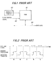
- Fig. 1 shows the conventional memory circuit which is used for the pipe line control, in which the data transfer and the memory processing (the writing of data into a memory and the reading of data from the memory) are carried out at the same stage.
- the conventional memory circuit comprises a RAM 41 connected with a R/W control signal line 42, an address pointer 43 for designating an address of the RAM 42, and a data bus 44 connected to the RAM 41.
- data transferred on the data bus 44 are written into addresses of the RAM 41 designated by the address pointer 43 in accordance with a write control signal supplied from the R/W control signal line 42 at pipe line control stages "n", "n+1” and "n+3", as shown in Fig. 2.
- data stored in the RAM 41 are read from addresses of the RAM 41 designated by the address pointer 43 to be transferred on the data bus 44 in accordance with a read control signal supplied from the R/W control signal line 42 at the pipe line control stages "n+2" and "n+4", as also shown in Fig. 2.
- Fig. 3 shows operation of the conventional memory circuit, in which the data transfer and the memory processing are carried out at different stages of the pipe line control.
- the reading of data D4 from the RAM 41 is carried out between the writing of data D1, D2 and D3 and the writing of data D5 and D6, so that the writing of the data D3 and the reading of the data D4 are carried out without data transfer at the pipe line stages "n+3" and "n+4", and the transfer of the data D4 and D5 is carried out without memory processing at the pipe line stages "n+5" and "n+6".
- N is a number, by which the writing or reading of data is consecutively carried out. If the number N is indefinitely large, the average time S becomes nearly equal to the time T.
- a time necessary for each stage is the sum of the data transfer and the memory processing in the conventional memory circuit. Therefore, the average access time is not shortened to be less than a value of the before described sum. For instance, when the data transfer on the data bus 44 takes 30 ns, and the memory processing (write into the RAM 41 or read from the RAM 41) takes 30 ns, each stage is not shortened to be less than 60 ns in the pipe line control operation. Therefore, even if a high speed operation is realized in logic devices other than the RAM 41 by the pipe line control, the conventional memory circuit hinders the high speed operation of a pipe line control system.
- the high speed operation of the pipe line control system is not hindered by logic devices such as logic calculation circuits, etc., but hindered by memory circuits and buses. Accordingly, a memory circuit which is accessed with high speed is required as realized in logic calculation circuits.
- a memory circuit of the first preferred embodiment according to the invention will be explained in Fig. 4.
- a RAM 1 of 24 bits having memory cells of 1024 words is provided to be designated in address by a predecoder 14, in which an address signal of an address pointer 2 positioned on an address bus 109 is decoded to be supplied to the RAM 1, to which data is written and from which data is read, respectively, by 40 ns.
- a first-in and first-out type (defined "FIFO” hereinafter) buffer 3 is of 24 bits and of a two-stage structure, and latches data of 24 bits supplied from a data bus 100 at the front stage thereof in response to an output signal of an AND gate 4 (FIFO input clock).
- FIFO first-in and first-out type
- Data output of the FIFO buffer 3 is carried out in response to an output signal of an AND gate 5 (FIFO output clock), so that data latched at the back stage of the FIFO buffer 3 is transfered to the RAM 1, and the back stage of the FIFO buffer 3 becomes a vacant state in accordance with the invalidation by a rising edge of the output signal of the AND gate 5.
- AND gate 5 FIFO output clock
- Signal lines 102 and 103 are provided to supply clock signals CL1 and CL2 having cycles of 40 ns to the predecoder 14 and other circuits, wherein the memory processing is carried out in the RAM 1 in synchronization with the clock signal CL2, and a latch 13 latches data read from the RAM 1 during a period of a rising edge of the clock signal CL2 to a following rising edge thereof.
- a R/W control signal line 104 is provided to supply a R/W control signal 104 (same reference numeral used) to a multiplexer 11, so that an address signal 105 of 10 bits supplied from an address calculation circuit 6 is determined for the data writing or the data reading. That is, the R/W control signal 104 of "low” instructs the conduct of the data reading, while the R/W control signal 104 of "high” instructs the conduct of the data writing.
- Write-address buffers 7 and 8 are provided to latch address signals of 10 bits on address buses 107 and 105 by rising edges of output signals supplied from AND gates 9 and 10.
- the write-address buffers 7 and 8 and the pointer 2 function as shift registers of 10 bits at the time of the data writing (the R/W control signal being "high").
- a multiplexer 11 is provided to transfer an address signal on the address bus 105 to the pointer 2 at the time of the data reading (the R/W control signal being "low"), and transfer an address signal on the address bus 106 to the pointer 2 at the time of the data writing.
- a comparator 140 is provided to supply a coincidence signal 110 to a D type flip flop 150 as a result of the comparison between one of address signals 106 and 107 latched in the write-address buffers 7 and 8 and an address signal 109 of the pointer 2, and the comparison is carried out by a rising edge of the clock signal CL 2.
- the coincidence signal 110 is of a bit arrangement of (1, 0), when the address signals 106 and 109 are coincided with each other, and the coincidence signal 110 is of (1, 1), when the address signals 107 and 109 are coincided with each other, while the coincidence signal 110 is of (0, x), when none of the address signals 106 and 107 is coincided with the address signal 109, where the bit "x" may be any value of "1" and "0".
- the coincidence signal 110 is delayed in the D type flip flop 150 by one clock, and is transferred to a multiplexer 12, to which the R/W control signal 104 is supplied through D type flip flops 151 to 153 to be delayed as a delayed signal 115 by 1.5 clocks.
- the coincidence signal 111 is of the bit arrangement of (1, x) to indicate that the both address signals 106 and 107 do not coincide with the address signal 109, the multiplexer 12 selects a data bus 114 connected to the latch 13.
- the multiplexer 12 selects a data but 113, and when the delayed signal 115 is "0", and the coincidence signal 111 is of (1, 1), the multiplexer 12 selects a data bus 112. On the contrary, when the delayed signal 115 is "high" to instruct the conduct of the data writing, the multiplexer is at a high impedance state.
- the D type flip flop 151 is supplied with the R/W control signal 104 to generate a mode designating signal which is "0" to shift the RAM 1 to the reading mode, and "1" to shift the RAM 1 to the writing mode.
- the address calculation circuit 6 calculates an address in accordance with address data on an address bus 101, so that an address signal thus calculated is supplied on the address bus 105 to indicate a write-address or a read-address.
- addresses a, b and c are calculated in the address calculation circuit 6 by receiving data on the address bus 101, and the addresses a, b and c are supplied on the address bus 105 as read-addresses, because the R/W control signal 104 is low. Consequently, the multiplexer 11 selects the address bus 105 in response to the R/W control signal 104 of "0", so that the read-addresses a, b and c are supplied through the multiplexer 11 to the pointer 2.
- the read-address a, b and c are supplied from the pointer 2 through the address bus 109 to the predecoder 102, so that address signals thus decoded are delayed to be supplied to the RAM 1 by 0.5 clock.
- the R/W control signal 104 is latched in the D type flip flop 151 in synchronization with the clock signal CL 2, so that the mode designating signal 120 is turned to be low.
- the RAM 1 is assumed to be under the reading mode, so that data a, b and c are read from the addresses a, b and c at the times of A′, B′ and C′.
- the read data a, b and c are latched in the latch 13 by rising edges of the clock signal CL 2, and transferred to the multiplexer 12.
- the delayed signal 115 is turned to be low in accordance with the R/W control signal 104 of "low", so that the multiplexer 12 selects the data bus 114 to transfer the data a, b and c from the latch 13 to the data bus 100.
- the writing mode is designated at the time of D, when the R/W control signal 104 is turned to be high.
- address data of "3FF H " is stored in the write-address buffers 7 and 8 at the initial state prior to operation, and that the address "3FF H " of the RAM 1 is an exclusively occupied area which is not used for effective data.
- addresses d, e and f are generated in the address calculation circuit 6 to be supplied on the address bus 105, and the multiplexer 11 selects the address bus 106 in response to the R/W control signal of "high".
- the pointer 2 and the write-address buffers 7 and 8 function as shift registers. That is, the pointer 2 latches data of the write-address buffer 7 at the time D, the write-address buffer 7 latches data of the write-address buffer 8 at a time which is behind the time D by a short time, and the write-address buffer 8 latches the address d.
- data shift is repeated in the pointer 2, and the write-address buffers 7 and 8 at the times of E and F. Subsequently, the address d is held at the time F.
- the R/W control signal 104 makes the mode designating signal 120 high, so that the RAM 1 is controlled to be under the data writing mode. Consequently, the data d on the data bus 100 is written into the address d of the RAM 1 during the time of F′ to G′.
- the data d is transferred on the data bus 100 after 1.5 clocks from the time when the address calculation circuit 6 generates the address d, and is latched at the front stage of the FIFO buffer 3 at the time F′.
- the back stage of the FIFO buffer 3 is vacant, so that the data d is instantly transferred to the back stage thereof to be supplied on the data bus 113.
- the RAM 1 is under the data writing mode, so that the data d is written into the address d of the RAM 1 before the time G′.
- the data d held at the back stage of the FIFO buffer 3 is invalidated to make it at a vacant state. Therefore, the next data e is supplied from the data bus 100 to be latched at the front stage of the FIFO buffer 3 at this time, and is instantly latched at the back stage thereof. Consequently, the data e is supplied on the data bus 113 at a time which is behind the time G′ by a short time.
- the R/W control signal is turned back to be low at the time G, so that the RAM 1 is again under the data reading mode.
- the data e is supplied to the data bus 100 at a time behind the time G′ by a short time.
- the addresses e and f which are generated in the address calculation circuit 6 at the times of E and F are held in the write-address buffers 7 and 8, and the pointer 2 holds a following read-address g at this time.
- the write-data f is supplied on the data bus 100 during a time of G′ to H′, and is latched at the front stage of the FIFO buffer 3 at the time H′.
- the data e has been already latched at the back stage of the FIFO buffer 3, so that the data f is kept to be latched at the front stage thereof.
- the RAM 1 is turned to be under the data reading mode, so that the data g and h read from the addresses g and h which are supplied from the address calculation circuit 6 to the pointer 2 are supplied on the data bus 100 with the delayed time of 1.5 clocks.
- write-addresses are held in the write-address buffers 7 and 8, and write-data are held at the front and back stages of the FIFO buffer 3.
- the consecutive timing relation is obtained between the address calculation and the data transfer, even if the data transfer and the memory processing are separated, as described above.
- the data writing mode and the data reading mode which are instructed alternately are carried out without the time-loss to realize the high speed operation in a pipe line control system.
- data to be stored is once held in the FIFO buffer 3, and thereafter written into the RAM 1 in the memory circuit of the first preferred embodiment according to the invention.
- data is written into the RAM 1 in accordance with a trigger signal which is an address signal for data to be written into the RAM 1 at a writing stage coming after the next writing stage.
- a trigger signal which is an address signal for data to be written into the RAM 1 at a writing stage coming after the next writing stage.
- data held in the FIFO buffer 3 is necessary to be once loaded on the data bus 100 prior to the writing thereof into the RAM 1.
- This case occurs when a calculated read-address coincides with read-addresses in the write-address buffers 7 and 8.
- data to be written is reloaded on the data bus 100 in accordance with a comparison result of the comparator 140 before writing the data into the RAM 1.
- the data of the FIFO buffer 3 is not invalidated to be written into the RAM 1.
- read-data or write-data for a calculated address is delayed to be transferred onto or from the data bus 100 by 1.5 clocks after the generation of the address.
- the timing does not depend on which mode is carried out between the writing and reading modes, and on the order of the two modes.
- an access to data of the RAM 1 is possible to be carried out by each 40 ns in this preferred embodiment. This can be realized, because the writing of data into the RAM 1 and the transfer of data to be written into the RAM 1 on the data bus 100 are separated and interposed. Such a separation of the transfer processing and the memory processing enhances the effectiveness of the pipe line control, and the average access time becomes half as compared to that in the conventional memory circuit.
- a memory capacity of the RAM 1, a bit width of the buffers, the pointer, the buses, etc. a frequency of the clock signals, etc. may be different from those of the preferred embodiment.
- Fig. 7 shows a memory circuit of a second preferred embodiment according to the invention, wherein like parts are indicated by like reference numerals, and a fixed value output circuit 31 and a multiplexer 32 are additionally provided.
- the fixed value output circuit 31 supplies a fixed value "3FF H " of 10 bits to the multiplexer 32, by which an output of the address calculation circuit 6 is selected, when a memory selection signal ( SEL ⁇ ) 300 is "0", and an output of the fixed value output circuit 31 is selected, when the memory selection signal 300 is "1".
- a R/W control signal 104 is supplied to an OR gate 33, to which the memory selection signal 300 is also supplied.
- the memory circuit when the memory circuit is not selected in the presence of the memory selection signal 300 of "1", the memory circuit operates in the same manner as the writing mode, so that data is written into a fixed value address of "3FF H " of the RAM 1, and no access is carried out to the RAM 1 other than the fixed value address.
- a data source (not shown) supplies all data to be written on the data bus 100, and dummy writing processing must be carried out by twice. This is because the data are written into the RAM 1 without being left in the FIFO buffer 3.
- the memory circuit comprises the shift registers and the FIFO buffer to absorb the alteration of the conduct order of the data transfer and the memory processing dependent on the difference between the writing and reading modes, so that the effectiveness of the pipe line control is enhanced. Accordingly, a processing time is largely reduced at each pipe line stage to shorten the average access time to the RAM. For instance, if a time necessary for the data transfer and a time necessary for the memory processing are assumed to be equal, a processing time becomes half at each stage of the pipe line control.
- the difference between the writing and reading modes is automatically absorbed in a hardware, so that there is an advantage in that an address is designated and data is supplied to a system data bus, respectively, at a constant timing without depending on the difference between the writing and reading modes. Therefore, the writing and reading modes are arranged in an arbitrary order, and the memory processing can be carried out, as if only the reading mode is carried out, because the writing mode is carried out as done in the reading mode by the pipe line processing.
Landscapes
- Engineering & Computer Science (AREA)
- Theoretical Computer Science (AREA)
- Physics & Mathematics (AREA)
- General Engineering & Computer Science (AREA)
- General Physics & Mathematics (AREA)
- Dram (AREA)
- Information Transfer Systems (AREA)
- Advance Control (AREA)
- Memory System (AREA)
- Static Random-Access Memory (AREA)
Applications Claiming Priority (2)
| Application Number | Priority Date | Filing Date | Title |
|---|---|---|---|
| JP417522/90 | 1990-12-28 | ||
| JP41752290A JP3191302B2 (ja) | 1990-12-28 | 1990-12-28 | メモリ回路 |
Publications (3)
| Publication Number | Publication Date |
|---|---|
| EP0493138A2 true EP0493138A2 (de) | 1992-07-01 |
| EP0493138A3 EP0493138A3 (de) | 1994-02-09 |
| EP0493138B1 EP0493138B1 (de) | 1998-07-08 |
Family
ID=18525613
Family Applications (1)
| Application Number | Title | Priority Date | Filing Date |
|---|---|---|---|
| EP91312091A Expired - Lifetime EP0493138B1 (de) | 1990-12-28 | 1991-12-30 | Speicherschaltung |
Country Status (4)
| Country | Link |
|---|---|
| US (1) | US5488712A (de) |
| EP (1) | EP0493138B1 (de) |
| JP (1) | JP3191302B2 (de) |
| DE (1) | DE69129739T2 (de) |
Cited By (1)
| Publication number | Priority date | Publication date | Assignee | Title |
|---|---|---|---|---|
| WO1994029870A1 (en) * | 1993-06-02 | 1994-12-22 | Microunity Systems Engineering, Inc. | A burst mode memory accessing system |
Families Citing this family (8)
| Publication number | Priority date | Publication date | Assignee | Title |
|---|---|---|---|---|
| US5696990A (en) * | 1995-05-15 | 1997-12-09 | Nvidia Corporation | Method and apparatus for providing improved flow control for input/output operations in a computer system having a FIFO circuit and an overflow storage area |
| US5790813A (en) * | 1996-01-05 | 1998-08-04 | Unisys Corporation | Pre-arbitration system allowing look-around and bypass for significant operations |
| US5838631A (en) | 1996-04-19 | 1998-11-17 | Integrated Device Technology, Inc. | Fully synchronous pipelined ram |
| US6567903B1 (en) | 1996-08-23 | 2003-05-20 | Emc Corporation | Data storage system having master/slave addressable memories |
| US6115320A (en) | 1998-02-23 | 2000-09-05 | Integrated Device Technology, Inc. | Separate byte control on fully synchronous pipelined SRAM |
| US7069406B2 (en) * | 1999-07-02 | 2006-06-27 | Integrated Device Technology, Inc. | Double data rate synchronous SRAM with 100% bus utilization |
| JP4749689B2 (ja) * | 2004-08-31 | 2011-08-17 | 三洋電機株式会社 | メモリ制御回路及びメモリ制御方法 |
| US20150095551A1 (en) * | 2013-09-30 | 2015-04-02 | Micron Technology, Inc. | Volatile memory architecutre in non-volatile memory devices and related controllers |
Family Cites Families (6)
| Publication number | Priority date | Publication date | Assignee | Title |
|---|---|---|---|---|
| JPS59136859A (ja) * | 1983-01-27 | 1984-08-06 | Nec Corp | バツフア制御装置 |
| JPS62126440A (ja) * | 1985-11-27 | 1987-06-08 | Nec Corp | 情報処理装置 |
| JP3255908B2 (ja) * | 1988-06-30 | 2002-02-12 | エルジー・セミコン・カンパニー・リミテッド | メモリー制御ユニット |
| US4882709A (en) * | 1988-08-25 | 1989-11-21 | Integrated Device Technology, Inc. | Conditional write RAM |
| JP2976429B2 (ja) * | 1988-10-20 | 1999-11-10 | 日本電気株式会社 | アドレス制御回路 |
| US5093809A (en) * | 1989-04-21 | 1992-03-03 | Siemens Aktiengesellschaft | Static memory having pipeline registers |
-
1990
- 1990-12-28 JP JP41752290A patent/JP3191302B2/ja not_active Expired - Fee Related
-
1991
- 1991-12-27 US US07/816,396 patent/US5488712A/en not_active Expired - Fee Related
- 1991-12-30 EP EP91312091A patent/EP0493138B1/de not_active Expired - Lifetime
- 1991-12-30 DE DE69129739T patent/DE69129739T2/de not_active Expired - Fee Related
Cited By (1)
| Publication number | Priority date | Publication date | Assignee | Title |
|---|---|---|---|---|
| WO1994029870A1 (en) * | 1993-06-02 | 1994-12-22 | Microunity Systems Engineering, Inc. | A burst mode memory accessing system |
Also Published As
| Publication number | Publication date |
|---|---|
| DE69129739D1 (de) | 1998-08-13 |
| JPH04279945A (ja) | 1992-10-06 |
| JP3191302B2 (ja) | 2001-07-23 |
| US5488712A (en) | 1996-01-30 |
| DE69129739T2 (de) | 1999-03-11 |
| EP0493138A3 (de) | 1994-02-09 |
| EP0493138B1 (de) | 1998-07-08 |
Similar Documents
| Publication | Publication Date | Title |
|---|---|---|
| KR100337052B1 (ko) | 동기화된 독출 포인터 및 기록 포인터를 갖는 2 중 포트 fifo | |
| US4463443A (en) | Data buffer apparatus between subsystems which operate at differing or varying data rates | |
| US7509469B2 (en) | Semiconductor memory asynchronous pipeline | |
| US5587953A (en) | First-in-first-out buffer memory | |
| US6279073B1 (en) | Configurable synchronizer for double data rate synchronous dynamic random access memory | |
| JP4315552B2 (ja) | 半導体集積回路装置 | |
| US5274600A (en) | First-in first-out memory | |
| US5291580A (en) | High performance burst read data transfer operation | |
| EP0493138A2 (de) | Speicherschaltung | |
| US7069406B2 (en) | Double data rate synchronous SRAM with 100% bus utilization | |
| US5781802A (en) | First-in-first-out (FIFO) controller for buffering data between systems which are asynchronous and free of false flags and internal metastability | |
| US5758131A (en) | Bus adapter for synchronizing communications between two circuits running at different clock rates | |
| US5033066A (en) | Event tagging time delay | |
| US5845314A (en) | Data storage apparatus, data reading apparatus and data transmission apparatus | |
| US6108244A (en) | Synchronous memory devices having dual port capability for graphics and other applications | |
| US6880050B1 (en) | Storage device, system and method which can use tag bits to synchronize queuing between two clock domains, and detect valid entries within the storage device | |
| US5267199A (en) | Apparatus for simultaneous write access to a single bit memory | |
| US5732011A (en) | Digital system having high speed buffering | |
| US20240013824A1 (en) | Data transmission apparatus and method having clock gating mechanism | |
| KR0181485B1 (ko) | 데이터 통신용 데이터 버퍼링 장치 | |
| US7899955B2 (en) | Asynchronous data buffer | |
| US5260909A (en) | Memory with phase locked serial input port | |
| JP3179891B2 (ja) | バス制御方式 | |
| KR100233100B1 (ko) | 시분할 액서스방식을 채용한 다중 프로세서의 데이타 통신장치 | |
| JPH06103026A (ja) | メモリシステム |
Legal Events
| Date | Code | Title | Description |
|---|---|---|---|
| PUAI | Public reference made under article 153(3) epc to a published international application that has entered the european phase |
Free format text: ORIGINAL CODE: 0009012 |
|
| 17P | Request for examination filed |
Effective date: 19920117 |
|
| AK | Designated contracting states |
Kind code of ref document: A2 Designated state(s): DE FR GB |
|
| PUAL | Search report despatched |
Free format text: ORIGINAL CODE: 0009013 |
|
| AK | Designated contracting states |
Kind code of ref document: A3 Designated state(s): DE FR GB |
|
| 17Q | First examination report despatched |
Effective date: 19970116 |
|
| GRAG | Despatch of communication of intention to grant |
Free format text: ORIGINAL CODE: EPIDOS AGRA |
|
| GRAG | Despatch of communication of intention to grant |
Free format text: ORIGINAL CODE: EPIDOS AGRA |
|
| GRAH | Despatch of communication of intention to grant a patent |
Free format text: ORIGINAL CODE: EPIDOS IGRA |
|
| GRAH | Despatch of communication of intention to grant a patent |
Free format text: ORIGINAL CODE: EPIDOS IGRA |
|
| GRAA | (expected) grant |
Free format text: ORIGINAL CODE: 0009210 |
|
| AK | Designated contracting states |
Kind code of ref document: B1 Designated state(s): DE FR GB |
|
| REF | Corresponds to: |
Ref document number: 69129739 Country of ref document: DE Date of ref document: 19980813 |
|
| ET | Fr: translation filed | ||
| PLBE | No opposition filed within time limit |
Free format text: ORIGINAL CODE: 0009261 |
|
| STAA | Information on the status of an ep patent application or granted ep patent |
Free format text: STATUS: NO OPPOSITION FILED WITHIN TIME LIMIT |
|
| 26N | No opposition filed | ||
| PGFP | Annual fee paid to national office [announced via postgrant information from national office to epo] |
Ref country code: FR Payment date: 20011212 Year of fee payment: 11 |
|
| REG | Reference to a national code |
Ref country code: GB Ref legal event code: IF02 |
|
| PGFP | Annual fee paid to national office [announced via postgrant information from national office to epo] |
Ref country code: GB Payment date: 20020102 Year of fee payment: 11 |
|
| PGFP | Annual fee paid to national office [announced via postgrant information from national office to epo] |
Ref country code: DE Payment date: 20020109 Year of fee payment: 11 |
|
| PG25 | Lapsed in a contracting state [announced via postgrant information from national office to epo] |
Ref country code: GB Free format text: LAPSE BECAUSE OF NON-PAYMENT OF DUE FEES Effective date: 20021230 |
|
| PG25 | Lapsed in a contracting state [announced via postgrant information from national office to epo] |
Ref country code: DE Free format text: LAPSE BECAUSE OF NON-PAYMENT OF DUE FEES Effective date: 20030701 |
|
| GBPC | Gb: european patent ceased through non-payment of renewal fee |
Effective date: 20021230 |
|
| PG25 | Lapsed in a contracting state [announced via postgrant information from national office to epo] |
Ref country code: FR Free format text: LAPSE BECAUSE OF NON-PAYMENT OF DUE FEES Effective date: 20030901 |
|
| REG | Reference to a national code |
Ref country code: FR Ref legal event code: ST |