EP0488802B1 - Anzeigevorrichtung mit aktiver Matrix - Google Patents
Anzeigevorrichtung mit aktiver Matrix Download PDFInfo
- Publication number
- EP0488802B1 EP0488802B1 EP91311143A EP91311143A EP0488802B1 EP 0488802 B1 EP0488802 B1 EP 0488802B1 EP 91311143 A EP91311143 A EP 91311143A EP 91311143 A EP91311143 A EP 91311143A EP 0488802 B1 EP0488802 B1 EP 0488802B1
- Authority
- EP
- European Patent Office
- Prior art keywords
- buses
- group
- active matrix
- display device
- etching stop
- Prior art date
- Legal status (The legal status is an assumption and is not a legal conclusion. Google has not performed a legal analysis and makes no representation as to the accuracy of the status listed.)
- Expired - Lifetime
Links
- 239000011159 matrix material Substances 0.000 title claims description 31
- 239000000758 substrate Substances 0.000 claims description 21
- 238000005530 etching Methods 0.000 claims description 13
- 229910021417 amorphous silicon Inorganic materials 0.000 claims description 12
- 229910004205 SiNX Inorganic materials 0.000 claims description 8
- 239000010410 layer Substances 0.000 description 39
- 239000010408 film Substances 0.000 description 30
- 229910052751 metal Inorganic materials 0.000 description 7
- 239000002184 metal Substances 0.000 description 7
- 238000000034 method Methods 0.000 description 5
- 239000004065 semiconductor Substances 0.000 description 5
- 230000009977 dual effect Effects 0.000 description 4
- 239000011241 protective layer Substances 0.000 description 4
- 239000004973 liquid crystal related substance Substances 0.000 description 3
- 238000004519 manufacturing process Methods 0.000 description 3
- 238000000059 patterning Methods 0.000 description 3
- 239000010409 thin film Substances 0.000 description 3
- 229910052782 aluminium Inorganic materials 0.000 description 2
- 229910052804 chromium Inorganic materials 0.000 description 2
- 230000007547 defect Effects 0.000 description 2
- 238000000151 deposition Methods 0.000 description 2
- 239000011521 glass Substances 0.000 description 2
- 238000009413 insulation Methods 0.000 description 2
- 238000005268 plasma chemical vapour deposition Methods 0.000 description 2
- 238000004544 sputter deposition Methods 0.000 description 2
- OAICVXFJPJFONN-UHFFFAOYSA-N Phosphorus Chemical compound [P] OAICVXFJPJFONN-UHFFFAOYSA-N 0.000 description 1
- 230000015572 biosynthetic process Effects 0.000 description 1
- 238000005229 chemical vapour deposition Methods 0.000 description 1
- 230000003247 decreasing effect Effects 0.000 description 1
- 230000002950 deficient Effects 0.000 description 1
- 239000012789 electroconductive film Substances 0.000 description 1
- AMGQUBHHOARCQH-UHFFFAOYSA-N indium;oxotin Chemical compound [In].[Sn]=O AMGQUBHHOARCQH-UHFFFAOYSA-N 0.000 description 1
- 239000000463 material Substances 0.000 description 1
- 229910044991 metal oxide Inorganic materials 0.000 description 1
- 150000004706 metal oxides Chemical class 0.000 description 1
- 229910052750 molybdenum Inorganic materials 0.000 description 1
- 230000003287 optical effect Effects 0.000 description 1
- 229910052698 phosphorus Inorganic materials 0.000 description 1
- 239000011574 phosphorus Substances 0.000 description 1
- 239000002356 single layer Substances 0.000 description 1
- 229910052715 tantalum Inorganic materials 0.000 description 1
- PBCFLUZVCVVTBY-UHFFFAOYSA-N tantalum pentoxide Inorganic materials O=[Ta](=O)O[Ta](=O)=O PBCFLUZVCVVTBY-UHFFFAOYSA-N 0.000 description 1
- 229910052719 titanium Inorganic materials 0.000 description 1
Images


Classifications
-
- G—PHYSICS
- G02—OPTICS
- G02F—OPTICAL DEVICES OR ARRANGEMENTS FOR THE CONTROL OF LIGHT BY MODIFICATION OF THE OPTICAL PROPERTIES OF THE MEDIA OF THE ELEMENTS INVOLVED THEREIN; NON-LINEAR OPTICS; FREQUENCY-CHANGING OF LIGHT; OPTICAL LOGIC ELEMENTS; OPTICAL ANALOGUE/DIGITAL CONVERTERS
- G02F1/00—Devices or arrangements for the control of the intensity, colour, phase, polarisation or direction of light arriving from an independent light source, e.g. switching, gating or modulating; Non-linear optics
- G02F1/01—Devices or arrangements for the control of the intensity, colour, phase, polarisation or direction of light arriving from an independent light source, e.g. switching, gating or modulating; Non-linear optics for the control of the intensity, phase, polarisation or colour
- G02F1/13—Devices or arrangements for the control of the intensity, colour, phase, polarisation or direction of light arriving from an independent light source, e.g. switching, gating or modulating; Non-linear optics for the control of the intensity, phase, polarisation or colour based on liquid crystals, e.g. single liquid crystal display cells
- G02F1/133—Constructional arrangements; Operation of liquid crystal cells; Circuit arrangements
- G02F1/136—Liquid crystal cells structurally associated with a semi-conducting layer or substrate, e.g. cells forming part of an integrated circuit
- G02F1/1362—Active matrix addressed cells
- G02F1/136286—Wiring, e.g. gate line, drain line
Definitions
- the present invention relates to a display device which forms a display by impressing drive signals on pixel electrodes used for display through switching elements, and more particularly to a display device which can perform a high density display by arranging pixel electrodes in a matrix.
- a liquid crystal display device, an EL display device and a plasma display device are known in the art in which pixel electrodes are selected and driven so as to display desired patterns on a screen.
- the display medium sealed between the electrodes is optically modulated by impressing a voltage between the selected pixel electrodes and the respective counter electrodes. The optical modulation is visually observed.
- An active matrix driving method is known as a driving method of pixel electrode. The active matrix driving method will be described.
- Pixel electrodes are independently arranged, and then provided with switching elements.
- the pixel electrodes are driven through the switching elements.
- TFTs thin film transistor
- MIMs metal-insulating layer-metal
- MOS transistors diodes
- varistors varistors and other known devices
- This type of active matrix method enables the display device to have a good contrast in the picture, and finds many applications such as in television, word processors, and display panels of computer terminals.
- buses are likely to be formed with the possibility of breakage during the fabrication of switching elements, buses, pixel electrodes on the active matrix substrate.
- a possible breakage of buses is detected as a line defect on the screen.
- the line defect is fatal for the display device.
- Defective display devices must be discarded, thereby decreasing production yield of display devices.
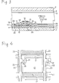
- Figure 6 shows an active matrix display which is driven by TFTs 31 .
- the active matrix has a structure made by two layers in which a conductive film wiring 23 is stacked on source buses 22 which cross over gate buses 21 .
- This active matrix has a dual structure which includes conductive film wiring 23 arranged on the source buses 22 . This dual structure is obtained by leaving the transparent conductive film on the source buses 22 after the source buses 22 are formed in pattern, when pixel electrodes 41 are formed with a transparent conductive film.
- the source buses 22 and the conductive film wirings 23 pass portions stepped by the gate buses at the junctions of the gate buses 21 and the source buses 22 , so that the source buses 22 and a conductive film wiring 23 are likely to break. This is caused by the fact that the source buses 22 and the conductive film wiring 23 do not fully cover the stepped portions made by the gate buses 21 , and that the source buses 22 and the conductive film wiring 23 are separated owing to poor adhesion of the insulating films to the gate buses 21 . The problem of leakage is nevertheless not solved by the dual structure.
- the etchant is likely to erode the metal parts of the source buses 22 .
- the source buses 22 are thus liable to breakage.
- EP-A-0 328 810 discloses a matrix-type liquid crystal display panel in which a source bus wiring pattern is covered by an electroconductive film of uniform width, similar to the arrangement shown in Figure 6.
- JP-A-60-236266 discloses, in relation to the formation of thin film layers in a thin film transistor, providing an upper layer which intersects a lower layer wherein the width of the upper layer is made greater at the portions which cross over the edges of the lower layer.
- the invention disclosed herein makes possible the objective of providing an active matrix display device which can maintain electric connection even in the case where the second group of buses are broken, thereby maintaining high production yield.
- the active matrix substrate includes the gate buses 21 in parallel with each other, the source buses 22 crossing the gate buses, and the conductive film wiring 23 .
- the substrate 1 also includes gate bus branch lines 25 branched from the gate buses 21 .
- the TFTs 31 are formed on the gate electrode 25 .
- the conductive film wiring 23 have a larger width on the stepped portions of the gate buses 21 than parts thereof located out of the stepped portions.
- a metal layer is deposited on the glass substrate by sputtering, and then it is formed into the gate buses 21 and the gate bus branch lines 25 by patterning.
- the metal layer instead of Ta, Ti, Al or Cr can be used, wherein the metal layer can be made as a single layer or a multi-layer. If necessary, the whole surface of the glass substrate can be coated with a base film of Ta2O5 or any other suitable metal oxide before the gate buses 21 are formed.
- the gate insulation film 11 is formed on the gate buses 21 by depositing SiNx as a film having a thickness of 300 nm by a plasma CVD method.
- the surfaces of the gate buses 21 and the gate bus branch line 25 can be anode-oxidized so as to enhance the insulating ability of the gate buses 21 and the gate bus branch lines 25 .
- the next step is that an intrinsic semiconductor amorphous silicon (hereinafter called "a-Si(i)”) layer, which eventually becomes a semiconductor layer 12 , and a SiNx layer, which functions as an etching stopper 13 , are successively deposited by a plasma CVD method.
- the a-Si(i) layer has a thickness of 30 nm and the SiNx layer has a thickness of 200 nm.
- a layer of amorphous silicon of n+ type containing P (phosphorus) hereinafter called a-Si(n+)
- the a-Si(n+) layer has a thickness of 80 nm.
- the semiconductor layer 12 and the contact layer 14 are formed by patterning the a-Si(n+) layer and the a-Si(i) layer.
- the contact layer 14 provides ohmic contact between the semiconductor layer 12 and the source electrode 32 and the drain electrode 33 , both of which are formed at a later stage.
- the source buses 22 , the source electrode 32 and drain electrode 33 are formed by depositing a Ti metal layer over the whole substrate 1 and then patterning it.
- a Ti metal layer instead of Ti, for example, Al, Mo, and Cr can be used for the metal layer.
- each conductive film wiring 23 is not narrower than the source bus 22 , and is overlaid on it. As shown in Figure 2 , at junctions where the gate buses 21 and the source buses 22 cross each other, the width of each conductive film wiring 23 at the stepped portion is larger than the width thereof located out of the stepped portions.
- a protective layer 17 of SiNx is formed over the whole surface of the substrate 1 .
- the protective layer 17 can be a window-open type; that is, the protective layer 17 is partly removed in a central portion of the pixel electrode.
- an orientation film 19 can be formed on the protective layer 17 .
- a counter substrate facing the active matrix substrate is fabricated with a counter electrode 3 and substrate is fabricated with a counter electrode 3 and an orientation film 9 on a substrate 2 .
- a liquid crystal layer 18 is placed and sealed between the counter electrode 3 and the substrate 1 . In this way, the active matrix display device is fabricated.
- the conductive film wiring 23 over any stepped portions at the junctions where the conductive film wiring 23 and the gate buses 21 cross each other has a relatively great width so that even if the source buses 22 break at the stepped portion, the broken source bus or buses can maintain an electric connection because of a lessened degree of breakage.
- This active matrix display device contains an additional capacitance 51 to hold charges stored in the pixel electrode.
- the additional capacitance 51 is formed between the pixel electrode 41 and an additional capacitance wiring 42 .
- the additional capacitance wiring 42 is formed at the same time as when the gate buses 21 are formed.
- the additional capacitance wiring 42 is located opposite to the pixel electrode 41 with the gate insulating film 11 sandwiched therebetween. The same signal is applied to the counter electrode 3 and the additional capacitance wiring 42 . Therefore the additional capacitance 51 and a pixel capacitance formed by the pixel electrode 41 and the counter electrode 3 become parallel.
- the conductive film wiring 23 is relatively wider over the stepped portions at the junctions where the conductive film wiring 23 and the gate buses 21 cross each other.
- the conductive film wirings 23 are relatively wide at the stepped portions at the junctions where the gate buses 21 and the additional capacitance wiring 42 cross each other.
- the additional capacitance wiring 42 prevents breakage of the conductive film wiring 23 .
- an a-Si(i) layer 44 and a SiNx layer 43 are held between the gate buses 21 and source buses 22 .
- the a-Si(i) layer 44 and the SiNx layer 43 are pattern-formed at the same time as when the semiconductor layer 12 and etching stopper 13 are formed.
- the insulating ability is enhanced between the gate buses 21 and source buses 22 .
- the conductive film wiring 23 at the stepped portions caused by the gate buses 21 has a width greater than the other parts thereof located out of the stepped portions.
- the conductive film wirings 23 are protected against breakage or at least they are less liable to breakage. Even if the source buses 22 breaks at the stepped portions, the electrical connection is advantageously maintained.
- a-Si(i) layer 44 and the SiNx layer 43 can be made of the same materials as that for the contact layer 14 .
- the active matrix substrates of the present invention find many applications such as in display devices using an MIM, an MOS, a transistor, a diode or a varistor as a switching element.
Landscapes
- Physics & Mathematics (AREA)
- Nonlinear Science (AREA)
- Mathematical Physics (AREA)
- Chemical & Material Sciences (AREA)
- Crystallography & Structural Chemistry (AREA)
- General Physics & Mathematics (AREA)
- Optics & Photonics (AREA)
- Engineering & Computer Science (AREA)
- Microelectronics & Electronic Packaging (AREA)
- Liquid Crystal (AREA)
- Thin Film Transistor (AREA)
- Devices For Indicating Variable Information By Combining Individual Elements (AREA)
Claims (8)
- Aktivmatrix-Anzeigevorrichtung mit einem Paar isolierender Substrate (1, 2), einer ersten Gruppe von Bussen (21), die auf einer Seite eines der isolierenden Substrate (1) ausgebildet sind, einer zweiten Gruppe von Bussen (22), die die erste Gruppe von Bussen (21) überkreuzen, und mit leitenden Streifen (23), die auf der zweiten Gruppe von Bussen ausgebildet sind, wobei die Breite jedes leitenden Streifens (23) größer als diejenige der zweiten Gruppe von Bussen (22) ist;
dadurch gekennzeichnet, daß- Ätzstoppschichten (44, 43) zwischen der ersten und zweiten Gruppe von Bussen (21, 22) an jedem Überkreuzungsabschnitt zwischen der ersten und zweiten Gruppe von Bussen angeordnet sind, die Breiten aufweisen, die größer als die der ersten und zweiten Gruppe von Bussen sind;- jeder leitende Streifen (23) dort erhöhte Breite aufweist, wo der leitende Streifen und jeder Bus der zweiten Gruppe von Bussen (22) eine Stufe über eine Kante jedes Busses der ersten Gruppe von Bussen (21) bilden; und- der verbreiterte Abschnitt jedes leitenden Streifens (23) einen Kantenabschnitt der Ätzstoppschichten (44, 43) überdeckt. - Aktivmatrix-Anzeigevorrichtung nach Anspruch 1, ferner mit einer jeweiligen Zusatzkapazität (51) zum Aufrechterhalten von in jeder Pixelelektrode (41) der Vorrichtung aufrechterhaltenen Ladungen, die mit einem leitenden Teil (42) versehen ist, das der Pixelelektrode gegenüberliegt und sich über die Breite derselben hinaus erstreckt, wobei die zweite Gruppe von Bussen (22) das leitende Teil (42) überkreuzt.
- Aktivmatrix-Anzeigevorrichtung nach Anspruch 2, bei der jeder leitende Streifen (23) dort erhöhte Breite aufweist, wo die leitenden Streifen und die zweite Gruppe von Bussen (22) über einer Kante des leitenden Teils (42) eine Stufe bilden.
- Aktivmatrix-Anzeigevorrichtung mit mehreren Pixelelektroden (41), einer jeweiligen Mehrzahl von Schaltelementen (31) zum Ansteuern der jeweiligen Pixelelektroden (41), einer ersten Gruppe von Bussen (21) und einer zweiten Gruppe von Bussen (22), die jeweilige erste und zweite Signale an die Schaltelemente führen, wobei die erste und zweite Gruppe von Bussen durch eine Isolierschicht (11, 44, 43) voneinander getrennt sind und sie in einer Gitteranordnung angeordnet sind, die eine Vielzahl von Schnittstellen erzeugt, an der die Busse (22) der zweiten Gruppe verformt sind, wenn sie die Busse (21) der ersten Gruppe überkreuzen, und mit mehreren leitenden Streifen (23), die jeweils auf einer Seite eines jeweiligen der Busse (22) der zweiten Gruppe liegen und in elektrischem Kontakt mit diesem stehen,
dadurch gekennzeichnet, daß- die Isolierschicht (11, 44, 43) Ätzstoppschichten (44, 43) enthält, die an jeder Schnittstelle der Busse (21) der ersten Gruppe und der Busse (22) der zweiten Gruppe angeordnet sind, wobei die Ätzstoppschichten (44, 43) eine größere Breite als die Busse (21, 22) der ersten und der zweiten Gruppe aufweisen;- jeder leitende Streifen (23) an solchen Positionen erhöhte Breite aufweist, die verformten Abschnitten der jeweiligen Busse (22) der zweiten Gruppe entsprechen; und- jeder Abschnitt des leitenden Streifens (23) mit erhöhter Breite einen Kantenabschnitt der entsprechenden Ätzstoppschichten (44, 43) überdeckt. - Aktivmatrix-Anzeigevorrichtung nach Anspruch 4, ferner mit einem leitenden Teil (42), das auf einer Seite jeder Pixelelektrode vorhanden ist und von der Elektrode über eine Isolierschicht (11) beabstandet ist, um eine Kapazität zum Aufrechterhalten der in der Pixelelektrode (41) abgespeicherten Ladungen zu schaffen, wobei sich das leitende Teil (42) über die Breite der Pixelelektrode hinaus erstreckt, wobei die Busse (22) der zweiten Gruppe verformt sind, wenn sie die leitenden Teile (42) überkreuzen, und jeder leitende Streifen (23) an solchen Positionen erhöhte Breite aufweist, die mit den so verformten Abschnitten der jeweiligen Busse (22) der zweiten Gruppe übereinstimmen.
- Aktivmatrix-Anzeigevorrichtung nach einem der vorstehenden Ansprüche, bei der die Ätzstoppschichten eine erste Schicht (44) aus a-Si(i) und eine zweite Schicht (43) aus Si-Nx aufweisen.
- Aktivmatrix-Anzeigevorrichtung nach Anspruch 6, bei der die zwei Ätzstoppschichten (44, 43) gemustert sind.
- Aktivmatrix-Anzeigevorrichtung nach einem der vorstehenden Ansprüche, bei der die Breite jedes leitenden Streifens (23) in den verbreiterten Abschnitten am größten ist, in denen die zweite Gruppe von Bussen (22) eine Stufe über den Kanten der ersten Gruppe von Bussen (21) bildet, und die Breite jedes leitenden Streifens (23) im Bereich der Ätzstoppschichten (44, 43), der von den verbreiterten Abschnitten abweicht, größer ist als die der Ätzstoppschichten.
Applications Claiming Priority (2)
| Application Number | Priority Date | Filing Date | Title |
|---|---|---|---|
| JP338881/90 | 1990-11-30 | ||
| JP33888190 | 1990-11-30 |
Publications (3)
| Publication Number | Publication Date |
|---|---|
| EP0488802A2 EP0488802A2 (de) | 1992-06-03 |
| EP0488802A3 EP0488802A3 (en) | 1992-10-28 |
| EP0488802B1 true EP0488802B1 (de) | 1996-02-28 |
Family
ID=18322267
Family Applications (1)
| Application Number | Title | Priority Date | Filing Date |
|---|---|---|---|
| EP91311143A Expired - Lifetime EP0488802B1 (de) | 1990-11-30 | 1991-11-29 | Anzeigevorrichtung mit aktiver Matrix |
Country Status (4)
| Country | Link |
|---|---|
| US (1) | US5287206A (de) |
| EP (1) | EP0488802B1 (de) |
| KR (1) | KR920010341A (de) |
| DE (1) | DE69117452T2 (de) |
Families Citing this family (10)
| Publication number | Priority date | Publication date | Assignee | Title |
|---|---|---|---|---|
| US5502583A (en) * | 1993-05-15 | 1996-03-26 | Nec Corporation | Liquid crystal display device capable of compensating for a positioning error between a drain line and a display electrode |
| KR0171102B1 (ko) * | 1995-08-29 | 1999-03-20 | 구자홍 | 액정표시장치 구조 및 제조방법 |
| US7122835B1 (en) * | 1999-04-07 | 2006-10-17 | Semiconductor Energy Laboratory Co., Ltd. | Electrooptical device and a method of manufacturing the same |
| JP4596101B2 (ja) * | 2000-10-18 | 2010-12-08 | 日本電気株式会社 | 液晶表示装置 |
| KR100491821B1 (ko) * | 2002-05-23 | 2005-05-27 | 엘지.필립스 엘시디 주식회사 | 액정표시장치용 어레이기판과 그 제조방법 |
| JP5397219B2 (ja) * | 2006-04-19 | 2014-01-22 | イグニス・イノベーション・インコーポレイテッド | アクティブマトリックス表示装置用の安定な駆動スキーム |
| CN104460150B (zh) * | 2014-12-09 | 2018-09-04 | 深圳市华星光电技术有限公司 | 阵列基板、液晶显示面板及该阵列基板的制造方法 |
| CN104503178A (zh) * | 2014-12-31 | 2015-04-08 | 京东方科技集团股份有限公司 | 一种阵列基板、其制备方法及显示装置 |
| CN109545799B (zh) * | 2018-11-09 | 2021-01-08 | 惠科股份有限公司 | 一种显示面板、制作方法和显示装置 |
| CN114815426A (zh) * | 2022-05-10 | 2022-07-29 | 广州华星光电半导体显示技术有限公司 | 阵列基板及显示面板 |
Family Cites Families (15)
| Publication number | Priority date | Publication date | Assignee | Title |
|---|---|---|---|---|
| JPS5982769A (ja) * | 1982-11-04 | 1984-05-12 | Seiko Epson Corp | 薄膜シリコントランジスタ |
| JPS59119322A (ja) * | 1982-12-27 | 1984-07-10 | Seiko Epson Corp | 液晶表示装置 |
| JPS60236266A (ja) * | 1984-05-10 | 1985-11-25 | Matsushita Electric Ind Co Ltd | 半導体装置 |
| EP0288011A3 (de) * | 1987-04-20 | 1991-02-20 | Hitachi, Ltd. | Flüssigkristallanzeigeeinrichtung und Steuerungsverfahren dafür |
| JPH01102434A (ja) * | 1987-10-15 | 1989-04-20 | Sharp Corp | マトリックス型液晶表示パネル |
| JPH0814668B2 (ja) * | 1988-02-16 | 1996-02-14 | シャープ株式会社 | マトリックス型液晶表示パネル |
| JP2740813B2 (ja) * | 1988-02-26 | 1998-04-15 | セイコープレシジョン株式会社 | 非晶質シリコン薄膜トランジシタアレイ基板 |
| JPH01282522A (ja) * | 1988-05-10 | 1989-11-14 | Hitachi Ltd | アクティブマトリックス回路基板とその製造方法及びそれを用いた画像表示装置 |
| JPH01283519A (ja) * | 1988-05-10 | 1989-11-15 | Sanyo Electric Co Ltd | 液晶表示装置 |
| JPH02156227A (ja) * | 1988-12-07 | 1990-06-15 | Sharp Corp | アクティブマトリクス表示装置の表示電極基板 |
| JPH02165125A (ja) * | 1988-12-20 | 1990-06-26 | Seiko Epson Corp | 表示装置 |
| JPH0786618B2 (ja) * | 1988-12-29 | 1995-09-20 | シャープ株式会社 | アクティブマトリクス表示装置 |
| JP2603716B2 (ja) * | 1989-02-22 | 1997-04-23 | シャープ株式会社 | アクティブマトリクス表示装置 |
| JPH0786619B2 (ja) * | 1989-04-26 | 1995-09-20 | シャープ株式会社 | アクティブマトリクス表示装置 |
| US5062690A (en) * | 1989-06-30 | 1991-11-05 | General Electric Company | Liquid crystal display with redundant FETS and redundant crossovers connected by laser-fusible links |
-
1991
- 1991-11-27 US US07/798,722 patent/US5287206A/en not_active Expired - Lifetime
- 1991-11-29 DE DE69117452T patent/DE69117452T2/de not_active Expired - Fee Related
- 1991-11-29 EP EP91311143A patent/EP0488802B1/de not_active Expired - Lifetime
- 1991-11-29 KR KR1019910021799A patent/KR920010341A/ko not_active Ceased
Also Published As
| Publication number | Publication date |
|---|---|
| US5287206A (en) | 1994-02-15 |
| EP0488802A2 (de) | 1992-06-03 |
| DE69117452T2 (de) | 1996-08-01 |
| DE69117452D1 (de) | 1996-04-04 |
| KR920010341A (ko) | 1992-06-26 |
| EP0488802A3 (en) | 1992-10-28 |
Similar Documents
| Publication | Publication Date | Title |
|---|---|---|
| US5162901A (en) | Active-matrix display device with added capacitance electrode wire and secondary wire connected thereto | |
| EP0772073B1 (de) | Flüssigkristall-Anzeigevorrichtung | |
| KR100923056B1 (ko) | 표시 장치 및 이의 제조방법 | |
| KR100493869B1 (ko) | 횡전계 방식의 액정표시장치 및 그 제조방법 | |
| EP0514218B1 (de) | Substrat mit aktiver Matrix | |
| GB2307087A (en) | Liquid crystal displays | |
| US5434686A (en) | Active matrix display device | |
| US4816885A (en) | Thin-film transistor matrix for liquid crystal display | |
| EP0488802B1 (de) | Anzeigevorrichtung mit aktiver Matrix | |
| US7023016B2 (en) | Thin film transistor array panel and manufacturing method thereof | |
| KR0128815B1 (ko) | 스위칭 소자 어레이 및 이를 이용한 액정표시장치 | |
| JPH04257826A (ja) | アクティブマトリクス基板の製造方法 | |
| JP3235540B2 (ja) | 液晶表示装置用薄膜トランジスタアレイおよびその製造方法 | |
| US5432625A (en) | Display screen having opaque conductive optical mask and TFT of semiconductive, insulating, and conductive layers on first transparent conductive film | |
| JP2800958B2 (ja) | アクティブマトリクス基板 | |
| KR20010056591A (ko) | 액정 표시장치 제조방법 및 그 제조방법에 따른액정표시장치 | |
| US5875009A (en) | Sequential staggered type thin film transistor | |
| KR20020011574A (ko) | 액정 표시 장치용 어레이 기판 및 그 제조 방법 | |
| JP2677714B2 (ja) | アクティブマトリクス基板およびその製造方法 | |
| JPH04338728A (ja) | アクティブマトリクス基板 | |
| US20040100434A1 (en) | Wire structure of display device | |
| JP2669512B2 (ja) | アクティブマトリクス基板 | |
| JPH0618929A (ja) | アクティブマトリクス基板の製造方法 | |
| KR20070080475A (ko) | 박막 트랜지스터 기판 및 액정 표시 장치 | |
| EP0335724A2 (de) | Dünnfilmtransistor-Array für ein elektrooptisches Bauelement und dessen Herstellungsverfahren |
Legal Events
| Date | Code | Title | Description |
|---|---|---|---|
| PUAI | Public reference made under article 153(3) epc to a published international application that has entered the european phase |
Free format text: ORIGINAL CODE: 0009012 |
|
| AK | Designated contracting states |
Kind code of ref document: A2 Designated state(s): DE FR GB NL |
|
| PUAL | Search report despatched |
Free format text: ORIGINAL CODE: 0009013 |
|
| AK | Designated contracting states |
Kind code of ref document: A3 Designated state(s): DE FR GB NL |
|
| 17P | Request for examination filed |
Effective date: 19930106 |
|
| 17Q | First examination report despatched |
Effective date: 19941005 |
|
| GRAA | (expected) grant |
Free format text: ORIGINAL CODE: 0009210 |
|
| AK | Designated contracting states |
Kind code of ref document: B1 Designated state(s): DE FR GB NL |
|
| REF | Corresponds to: |
Ref document number: 69117452 Country of ref document: DE Date of ref document: 19960404 |
|
| ET | Fr: translation filed | ||
| PLBE | No opposition filed within time limit |
Free format text: ORIGINAL CODE: 0009261 |
|
| STAA | Information on the status of an ep patent application or granted ep patent |
Free format text: STATUS: NO OPPOSITION FILED WITHIN TIME LIMIT |
|
| 26N | No opposition filed | ||
| PGFP | Annual fee paid to national office [announced via postgrant information from national office to epo] |
Ref country code: FR Payment date: 20011113 Year of fee payment: 11 |
|
| PGFP | Annual fee paid to national office [announced via postgrant information from national office to epo] |
Ref country code: GB Payment date: 20011128 Year of fee payment: 11 |
|
| PGFP | Annual fee paid to national office [announced via postgrant information from national office to epo] |
Ref country code: NL Payment date: 20011129 Year of fee payment: 11 |
|
| PGFP | Annual fee paid to national office [announced via postgrant information from national office to epo] |
Ref country code: DE Payment date: 20011217 Year of fee payment: 11 |
|
| REG | Reference to a national code |
Ref country code: GB Ref legal event code: IF02 |
|
| PG25 | Lapsed in a contracting state [announced via postgrant information from national office to epo] |
Ref country code: GB Free format text: LAPSE BECAUSE OF NON-PAYMENT OF DUE FEES Effective date: 20021129 |
|
| PG25 | Lapsed in a contracting state [announced via postgrant information from national office to epo] |
Ref country code: NL Free format text: LAPSE BECAUSE OF NON-PAYMENT OF DUE FEES Effective date: 20030601 |
|
| PG25 | Lapsed in a contracting state [announced via postgrant information from national office to epo] |
Ref country code: DE Free format text: LAPSE BECAUSE OF NON-PAYMENT OF DUE FEES Effective date: 20030603 |
|
| GBPC | Gb: european patent ceased through non-payment of renewal fee | ||
| PG25 | Lapsed in a contracting state [announced via postgrant information from national office to epo] |
Ref country code: FR Free format text: LAPSE BECAUSE OF NON-PAYMENT OF DUE FEES Effective date: 20030731 |
|
| NLV4 | Nl: lapsed or anulled due to non-payment of the annual fee |
Effective date: 20030601 |
|
| REG | Reference to a national code |
Ref country code: FR Ref legal event code: ST |