EP0488031B1 - Méthode et dispositif pour inspecter un circuit imprimé - Google Patents
Méthode et dispositif pour inspecter un circuit imprimé Download PDFInfo
- Publication number
- EP0488031B1 EP0488031B1 EP91119738A EP91119738A EP0488031B1 EP 0488031 B1 EP0488031 B1 EP 0488031B1 EP 91119738 A EP91119738 A EP 91119738A EP 91119738 A EP91119738 A EP 91119738A EP 0488031 B1 EP0488031 B1 EP 0488031B1
- Authority
- EP
- European Patent Office
- Prior art keywords
- image
- hole
- gauge
- pattern
- size
- Prior art date
- Legal status (The legal status is an assumption and is not a legal conclusion. Google has not performed a legal analysis and makes no representation as to the accuracy of the status listed.)
- Expired - Lifetime
Links
Images


Classifications
-
- G—PHYSICS
- G06—COMPUTING; CALCULATING OR COUNTING
- G06T—IMAGE DATA PROCESSING OR GENERATION, IN GENERAL
- G06T1/00—General purpose image data processing
-
- G—PHYSICS
- G06—COMPUTING; CALCULATING OR COUNTING
- G06T—IMAGE DATA PROCESSING OR GENERATION, IN GENERAL
- G06T7/00—Image analysis
- G06T7/0002—Inspection of images, e.g. flaw detection
- G06T7/0004—Industrial image inspection
- G06T7/0006—Industrial image inspection using a design-rule based approach
-
- G—PHYSICS
- G01—MEASURING; TESTING
- G01N—INVESTIGATING OR ANALYSING MATERIALS BY DETERMINING THEIR CHEMICAL OR PHYSICAL PROPERTIES
- G01N21/00—Investigating or analysing materials by the use of optical means, i.e. using sub-millimetre waves, infrared, visible or ultraviolet light
- G01N21/84—Systems specially adapted for particular applications
- G01N21/88—Investigating the presence of flaws or contamination
- G01N21/95—Investigating the presence of flaws or contamination characterised by the material or shape of the object to be examined
- G01N21/956—Inspecting patterns on the surface of objects
-
- G—PHYSICS
- G01—MEASURING; TESTING
- G01R—MEASURING ELECTRIC VARIABLES; MEASURING MAGNETIC VARIABLES
- G01R31/00—Arrangements for testing electric properties; Arrangements for locating electric faults; Arrangements for electrical testing characterised by what is being tested not provided for elsewhere
- G01R31/28—Testing of electronic circuits, e.g. by signal tracer
- G01R31/302—Contactless testing
- G01R31/308—Contactless testing using non-ionising electromagnetic radiation, e.g. optical radiation
- G01R31/309—Contactless testing using non-ionising electromagnetic radiation, e.g. optical radiation of printed or hybrid circuits or circuit substrates
-
- G—PHYSICS
- G06—COMPUTING; CALCULATING OR COUNTING
- G06T—IMAGE DATA PROCESSING OR GENERATION, IN GENERAL
- G06T7/00—Image analysis
- G06T7/60—Analysis of geometric attributes
- G06T7/62—Analysis of geometric attributes of area, perimeter, diameter or volume
-
- G—PHYSICS
- G01—MEASURING; TESTING
- G01N—INVESTIGATING OR ANALYSING MATERIALS BY DETERMINING THEIR CHEMICAL OR PHYSICAL PROPERTIES
- G01N21/00—Investigating or analysing materials by the use of optical means, i.e. using sub-millimetre waves, infrared, visible or ultraviolet light
- G01N21/84—Systems specially adapted for particular applications
- G01N21/88—Investigating the presence of flaws or contamination
- G01N21/95—Investigating the presence of flaws or contamination characterised by the material or shape of the object to be examined
- G01N21/956—Inspecting patterns on the surface of objects
- G01N2021/95638—Inspecting patterns on the surface of objects for PCB's
- G01N2021/95646—Soldering
-
- G—PHYSICS
- G01—MEASURING; TESTING
- G01N—INVESTIGATING OR ANALYSING MATERIALS BY DETERMINING THEIR CHEMICAL OR PHYSICAL PROPERTIES
- G01N21/00—Investigating or analysing materials by the use of optical means, i.e. using sub-millimetre waves, infrared, visible or ultraviolet light
- G01N21/84—Systems specially adapted for particular applications
- G01N21/88—Investigating the presence of flaws or contamination
- G01N21/95—Investigating the presence of flaws or contamination characterised by the material or shape of the object to be examined
- G01N21/956—Inspecting patterns on the surface of objects
- G01N2021/95638—Inspecting patterns on the surface of objects for PCB's
- G01N2021/95653—Through-holes
-
- G—PHYSICS
- G06—COMPUTING; CALCULATING OR COUNTING
- G06T—IMAGE DATA PROCESSING OR GENERATION, IN GENERAL
- G06T2207/00—Indexing scheme for image analysis or image enhancement
- G06T2207/30—Subject of image; Context of image processing
- G06T2207/30108—Industrial image inspection
- G06T2207/30141—Printed circuit board [PCB]
Definitions
- THE PRESENT INVENTION relates to a method of and an apparatus for inspecting the minimum annular width of a land formed on a printed circuit board, and more particularly to an improvement to reconcile accuracy and speed in the inspection.
- a printed circuit board is formed with wiring patterns having lands and through holes.
- Automatic inspection apparatus for the printed circuit board to automatically inspect the relative positions of the wiring patterns and through holes by reading the image of the printed circuit board have been developed and put to practical use.
- One of the significant points in the printed circuit board inspection is to check that a minimum annular width of a land remains after forming a through hole therein.
- Figure 28 illustrates an example of the conventional inspection of annular width of a land.
- a through hole 2 is formed in a land 1.
- the through hole 2 is deviated from the centre of the land 1 resulting from a drilling error or the like.
- binary images of a wiring pattern including the land 1 and the through hole 2 are obtained.
- a radial operator 3 is positioned such that its centre coincides with the centre of the through hole 2.
- a logical operation is performed between the radial operator 3 and the image of the wiring pattern.
- the radial operator 3 has a plurality of arms. The annular widths of the land of the wiring pattern in the elongated directions of the respective arms are determined using a logic operation.
- a minimum annular width W L is obtained which is the minimum value among the respective annular widths.
- a threshold value it is determined that the printed circuit board is defective.
- the direction in which the through hole 2 deviates from the centre of the land 1 is not constant and varies in respective printed boards to be inspected.
- the high number of arms causes the time period required for the logic operation to grow longer so that the inspection is prevented from being performed at a high speed.
- Another problem is that the costs for manufacturing the inspection apparatus rise.
- the present invention is directed to a method of, and an apparatus for, inspecting the minimum annular width of a land formed on a printed circuit board.
- the printed board is provided thereon with a wiring pattern having the land and a through hole surrounded by the land.
- the present invention provides a method according to claim 1.
- Dependent claims 2-8 set out particular embodiment of this method.
- the invention provides an apparatus for inspecting the minimum annular width of a land formed on a printed circuit board which is provided thereon with a wiring pattern having said land and a through hole perfectly or imperfectly surrounded by said land according to claim 9.
- Dependent claims 10-16 set out particular embodiments of this apparatus.
- the deviation of the centre of the through hole from the centre of the land is in complementary relation to the minimum annular width, which is defined as the minimum value among annular widths at respective positions on the land. That is, the former is small when the latter is large, and vice versa.
- the minimum annular width is large, the deviation of the centre of the through hole from the centre of the land is small, so that the hole gauge image having the isotropic contour does not protrude or protrudes slightly from the pattern gauge image having the contour of the same shape as the pattern image. Accordingly, the size of the protrusion region image is zero or small.
- the size of the protrusion region image is large.
- the size of the protrusion region image is compared with the reference value to decide whether the minimum annular width is sufficient or not.
- the process step of comparing the size of the protrusion region image with the reference value may be attained by applying an operator having a size corresponding to the reference value to the protrusion region image.
- the minimum annular width is inspected by inspecting the size of the protrusion region image without applying a radial operator having arms to the land itself, the minimum annular width can be accurately inspected regardless of the direction in which the through hole is deviated from the land. Thus, a high-speed inspection can be achieved.
- An automatic inspection device for the printed circuit board when applied to the present invention, does not need a complicated circuit which causes costs to rise.
- the minimum annular width is inspected simply and accurately.
- the reference value may be variable. In this case, the sizes of the operator and ring-like image are accordingly changed. This prevents the false detection resulting from the broken pattern image when the minimum annular width is extremely small.
- the hole gauge image is defined by enlarging the hole image, the substantial decrease of the minimum annular width due to employment of the first enlarged hole image can be eliminated to achieve a more accurate inspection.
- the pattern gauge image is defined by a corrected image obtained by combining the pattern image and the hole image, a false detection around the hole is prevented.
- the corrected image may be thickened and then shrinked to obtain the pattern gauge image, so that a gap which may appear in the corrected gauge image is eliminated to achieve a more accurate inspection.
- Preferred embodiments of the present invention provide a method of and an apparatus for inspecting the minimum annular width of a land on a printed circuit board accurately at a high speed.
- a preferred embodiment of the present invention provides an apparatus for inspecting a printed board which can be obtained at a low cost.
- Fig. 4 schematically shows an image reading unit of an automatic inspection device for a printed circuit board according to a preferred embodiment of the present invention.
- a printed circuit board 10 is formed with a conductive wiring pattern 12 on one or both surfaces of an insulative base plate 11.
- the wiring pattern 12 includes a line part 13 and a land 14.
- the through hole 15 shown in Figs. 4 and 5 is a normal through hole for mounting electronic parts therethrough, which has a relatively large diameter.
- a through hole of another type is a mini via hole for connection between both surfaces of the printed circuit board 10, which has a relatively small diameter. Both the normal through hole and the mini via hole are generically referred to as "through holes" in the present invention.
- a transmission light source 21 is disposed below the printed circuit board 10, while reflection light sources 22 are disposed above the printed circuit board 10.
- Light from the transmission light source 21 passes through the through hole 15 to reach an optical head 20.
- Light from the reflection light sources 22 is reflected from the surface of the printed circuit board 10 to reach the optical head 20.
- the transmission and reflection light sources 21 and 22 are adapted to emit lights having different wavelengths.
- the lights pass through an image-formation lens system provided in the optical head 20 and are separated from each other by a dichroic mirror.
- Two CCD arrays also provided in the optical head 20 detect the separated lights, respectively.
- the pattern image signal PS O and the hole image signal HS O are delivered to binarizing circuits 31 and 32 of Fig. 6, respectively.
- the binarizing circuit 31 binarizes the pattern image signal PS O by comparing the pattern image signal PS O with a first threshold value TH1 shown in Fig. 7(a) to produce a digital pattern image signal PS.
- the binarizing circuit 32 compares the hole image signal HS O with a second threshold value TH2 to convert the hole image signal HS O into a digital hole image signal HS binarized.
- a blank portion PS H (Fig. 8) of the pattern image represented by the pattern image signal PS should be equal to that of a hole image HI represented by the hole image signal HS.
- the edge portions of the analog hole image signal HS O are inclined as shown in Fig. 7(b) resulting from light reflection from the inner wall of the through hole 15 and the like.
- the size of the obtained hole image HS is not equal to and is smaller than that of the blank portion PS H as shown in Fig. 9.
- the binarized pattern image signal PS and hole image signal HS are delivered to a pre-processor 100.
- the pre-processor 100 produces signals CHS t , CHS m , SHS t and SHS m , which will be described later, to output them to a land inspection circuit 200.
- the pattern image signal PS and the hole image signal HS are also inputted to the land inspection circuit 200.
- the details of the land inspection circuit 200 will be also described later.
- the inspection result of the land inspection circuit 200 is outputted as an inspection result signal INS c .
- the pre-processor 100 supplements and reshapes the blank portion of the pattern image by performing a compensation processing on the pattern image signal PS to thereby produce a corrected pattern image signal CPS.
- the corrected pattern image signal CPS is supplied to a DRC (Design Rule Check) circuit 310 and to a comparative inspection circuit 320.
- the DRC circuit 310 extracts the characteristics of the pattern image and compares them with the CAD data of the printed circuit board.
- the comparative inspection circuit 320 compares the pattern image of the printed circuit board to be inspected with a non-defective pattern image previously stored in an image memory 330 to execute an appearance inspection of the printed circuit board.
- the inspection results of the circuits 310 and 320 are outputted as inspection result signals INS a and INS b , respectively.
- the hole image signal HS is given to a recognition circuit 112 in a recognition and classification circuit 110.
- the recognition circuit 112 detects the diameter of the through hole 15 by applying a cross-shaped operator to the hole image and recognizes whether the through hole 15 is a normal through hole or a mini via hole by comparing the diameter with a predetermined threshold value.
- the recognition result is indicated by a signal S m .
- the signal S m and the hole image signal HS are outputted to a mini via hole elimination circuit 113.
- the mini via hole elimination circuit 113 fills in the inside of the mini via hole to thereby produce a hole image signal HS t including only the normal through hole.
- the hole image signal HS is also sent to a delay circuit 111 and is delayed therein, so that timing is adjusted between the hole image signal HS and the signal HS t .
- the logical product of an inversion signal of the signal HS t and the signal HS is obtained in an AND circuit 114.
- a logical product signal HS m is a hole image signal including only the mini via hole.
- the hole image signals HS t and HS m are inputted to an enlargement circuit 120.
- the hole image signal HS m representative of the mini via hole is enlarged by the width of a predetermined number of pixels, e.g., by the width of one pixel, in an enlargement circuit 121 to be converted into the first enlarged hole image signal CHS m for the mini via hole.
- the first enlarged hole image signal CHS m is further enlarged in an enlargement circuit 123 to be converted into the second enlarged hole image signal SHS m .
- the first enlarged hole image signal CHS m which is subjected to a timing adjustment in a delay circuit 122 and the second enlarged hole image signal SHS m are outputted to the exterior of the enalrgement circuit 120.
- the hole image signal HS t representative of the normal through hole is enlarged by the width of a predetermined number of pixels, e.g., by the width of one pixel, in an enlargement circuit 124 to be converted into the first enlarged hole image signal CHS t for the normal through hole.
- the first enlarged hole image signal CHS t is further enlarged in an enlargement circuit 126 to be converted into the second enlarged hole image signal SHS t .
- the first enlarged hole image signal CHS t which is subjected to a timing adjustment in a delay circuit 125 and the second enlarged hole image signal SHS t are outputted from the enlargement circuit 120.
- Fig. 11 is a block diagram of the internal structure of the enlargement circuit 126 for executing the second enlargement on the hole image of the normal through hole.
- the enlargement circuit 123 for the mini via hole has the same structure.
- the enlargement circuit 126 includes one-pixel enlargement circuits 131a to 131n for further enlarging the first enlarged hole image by the width of one pixel in sequential order.
- the number of one-pixel enlargement circuits 131a to 131n is, for example, twenty. All but the last one-pixel enlargement circuit 131n are fitted with delay circuits 132a to 132(n-1) for timing adjustment.
- the one-pixel enlargement circuits 131a to 131n are connected in series, and the respective outputs thereof are given to a selector 133 in parallel.
- Each of the one-pixel enlargement circuits 131a to 131n is adapted to perform a one-pixel enlargement processing in accordance with eight-point neighborhood enlargement logic, for example.
- the printed circuit board inspection apparatus is equipped with a control panel 50. Through manual operation of the control panel 50, a reference value designation signal QR and an operator size designation signal QS described later are inputted to a selection signal generator 51.
- the selection signal generator 51 produces a selection signal SEL1 based on the operator size designation signal QS to send it to the selector 133.
- the selector 133 outputs one of the n-number of enlarged hole image signals in response to the selection signal SEL1 as the second enlarged hole image signal SHS t .
- the enlargement circuits 126 and 123 are variable enlargement circuits capable of changing the enlargement width.
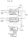
- Fig. 12 is a block diagram of part of the land inspection circuit 200 relevant to the preferred embodiment of the present invention.
- the land inspection circuit 200 includes an annular width inspection circuit 200t for the normal through hole and an annular width inspection circuit 200m for the mini via hole.
- the annular width inspection circuits 200t and 200m have the same internal structure and hold different data values such as reference values for inspecting the annular widths of through holes. Although only the annular width inspection circuit 200t is described hereinafter, the structure and the operation of the other circuit 200m will be understood by those skilled in the art from the following description.
- a pattern gauge signal PGS is obtained from the pattern image signal PS.
- the pattern gauge signal PGS is identical to the pattern signal PS in the preferred embodiment, the pattern gauge signal PGS may be a signal not identical but similar to the pattern signal PS.
- the pattern gauge signal PGS represents a pattern gauge image PGI, which is identical to the pattern image PI, in the preferred embodiment.
- the pattern gauge image signal PGS is inverted and input in an AND circuit 202. Another input of the and circuit 202 is a hole gauge signal HGS representing a hole gauge image HGI.
- the hole gauge image HGI is a ring-like image RI, which is obtained by taking a logical product of an inversion signal of the first enlarged hole image signal CHS t and the second enlarged hole image signal SHS t .
- the output signal HGS (RIS) of the AND circuit 201 represents the ring-like image RI obtained by removing the first enlarged hole image EH1 from the second enlarged hole image EH2.
- the pattern gauge image PGI and the hole gauge image HGI reflect the shapes of the pattern image PI and the hole image HI, respectively.
- the AND circuit 202 When the inversion signal of the pattern gauge signal PGS and the hole gauge signal HGS are applied to the AND circuit 202, the AND circuit 202 outputs a signal ES.
- the signal ES is a "protrusion region image signal" representative of part of the hole gauge image HGI which does not overlap the pattern gauge image PGI, that is, representative of a region ER protruding from the pattern gauge image PGI in the hole gauge image HGI.
- the protrusion region image signal ES is input to a two-dimensional shift register 210 for each pixel in series.
- the two-dimensional shift register 210 includes four one-line delay circuits 211 to 214 and twenty-five unit registers R11 to R55 arranged in a 5x5 matrix form. Outputs S11 to S55 from the unit registers R11 to R55 correspond to the two-dimensional protrusion region image signal ES in a 5x5 pixel arrangement. The signals S11 to S55 are transmitted to an operator circuit 220 (Fig. 1) in parallel.
- the operator circuit 220 includes AND circuits 221 to 225 and a selector 226, as shown in Fig. 14.
- the AND circuit 221 receives the signals S22, S23, S32 and S33 constituting a 2x2 pixel matrix OP4 and outputs the logical product PD4 of the signals to the selector 226. Only when the pixel matrix OP4 is positioned on a protrusion region image EI of Fig. 1, the logical product PD4 is "1". For this reason, the pixel matrix OP4 is an operator for a 2x2 pixel arrangement.
- the other AND circuits 222 to 225 operate similarily to the AND circuit 221.
- an operator OP9 for a rectangular cluster of nine pixels, an operator OP12 for a cross-shaped cluster of twelve pixels, an operator OP16 for a rectangular cluster of sixteen pixels, and an operator OP25 for a rectangular cluster of twenty-five pixels are applied to the protrusion region image EI, their outputs are given to the selector 226 as logical product signals PD9, PD12, PD16 and PD25, respectively.
- the signal S33 is also inputted to the selector 226 as a signal PD1.
- the signal PD1 corresponds to the operation result of an operator OP1 having only one pixel.
- the selection signal generator 51 of Fig. 12 produces a selection signal SEL2 in response to the reference value designation signal QR and operator size designation signal QS and outputs the selection signal SEL2 to the selector 226 of Fig. 14.
- the selector 226 selects one of the input signals PD1 to PD25 in response to the designation of the selection signal SEL2 to output the selected signal as the inspection result signal INS c .
- This electrical operation corresponds to an operation for determining the minimum annular width of the through hole. The reason therefor will be described later in detail.
- the operators OP1 to OP25 are represented by the reference character "OP”
- the logical product signals PD1 to PD25 are represented by the reference character "PD”.
- the operator OP corresponds to an approximately circular small region as shown in Fig. 15 since it is composed of a cluster of pixels.
- the logical product of "1" which is the result of applying the operator OP to the protrusion region image EI means that the size of the protrusion region image EI is larger than that of the operator OP. Since the center of the hole gauge image HGI coincides with the center of the through hole 15, the protrusion region image EI of large size is equivalent to the large deviation of the through hole 15 from the center of the land 14 so that the minimum annular width of the land 14 is small.
- the size of the protrusion region image EI is small.
- the whole operator OP is not present within the protrusion region image EI, so that the result of applying the operator OP to the protrusion region image EI is constantly "0".
- the signal PD of "1" is detected while the operator OP is scanning the protrusion region image EI, it is concluded that the minimum annular width is insufficient and the printed board is defective.
- the signal PD is always "0" during the scan, it is concluded that the minimum annular width is sufficient and the printed board is not defective.
- the scanning by the operator OP on the protrusion region image EI is automatically achieved by the scanning for reading the image of the printed circuit board 10.
- the operator OP is a perfectly or approximately isotropic circle in shape. It is, however, difficult to provide a perfectly circular operator in the digital signal processing.
- the rectangular operators or the cross-shaped operators obtained by removing the pixels at the corners from the rectangular operators are employed as approximately circular operators.
- the ring-like image RI described with reference to Fig. 1 may be used as the hole gauge image HGI.
- the width L is defined as the ring width of the ring-like image RI.
- the hole image HI and the blank portion PS H of the pattern image PI do not exactly coincide as discussed with reference to Fig. 9, it is assumed that they coincide approximately.
- the circumference of the blank portion PS H of the pattern image PI is taken as the circumference of the through hole 15.
- an enlarged hole image EHI is used as the hole gauge image HGI, as described below.
- the width L may be considered as the result of subtracting the radius of the through hole 15 (the radius of the hole image) from the radius of the enlarged hole image EHI.
- a condition for ensuring the necessary minimum annular width is: L a ⁇ L 0 where L0 is a reference value of the minimum annular width.
- the width L of the hole gauge image HGI and the size L r of the operator OP are determined so that the difference therebetween is equal to the reference value L O of the minimum annular width.
- This provides the result of "insufficient minimum annular width” because the formula (5) does not hold when the quantity L b is plus as shown in Fig. 17.
- the result of "sufficient annular width” is obtained because the formula (5) holds when L b is substantially minus as shown in Fig. 18.
- the signal QR representative of this value is input to the selection signal generator 51.
- the selection signal generator 51 calculates the width L of the hole gauge image HGI and the size L r of the operator OP according to the formula (6).
- the width L is uniquely determined from the formula (6). This determination can be achieved by storing a table corresponding to the formula (6) in the selection signal generator 51. Preferably, different sets of values (L, L r , L0) are used for the normal through hole and the mini via hole.
- the hole gauge image HGI and the pattern gauge image PGI are used for obtaining the protrusion region image EI. Since the peripheral portion of the hole gauge image HGI is relevant to the protrusion region image EI as mentioned above, the ring-like image RI shown in Fig. 1 can be used as the hole gauge image HGI.
- the principle for generating the ring-like image RI is as follows:
- the size of the hole image HI is sometimes smaller than that of the blank portion PS H of the pattern image PS because of light reflection or light scattering at the inner wall of the through hole 15.
- the hole image HI itself is employed in place of the enlarged hole image EH1 for generating the ring-like image RI of Fig. 1
- the size of a blank portion inside the ring-like image RI is smaller than that of the blank portion PS H of the pattern image PS, so that the output signal ES (Fig. 1) of the AND circuit 202 represents not only the protrusion region image EI but also an internal ring image NI, as shown in Fig. 26.
- the ring-like image RI based on the difference between the first and second enlarged hole images EH1 and EH2 determined in advance as shown in Fig. 1 is employed, the blank portion PS H of the pattern image PI is prevented from overlapping the ring-like image RI as shown in Fig. 27.
- This operation is advantageous in that the inspection for determining the defective/non-defective in the minimum annular width can be accurately performed.
- the ring-like image RI may be produced based on the difference between the enlarged ring-like image EH2 and the hole image HI itself.
- the ring-like image RI may be produced based cn the difference between the enlarged ring-like image EH2 and the hole image HI itself since the inspection result is not affected by the internal ring image NI.
- Figs. 2 and 3 show preferred embodiments in which the enlarged hole image EHI is used as the hole gauge image HGI.
- the corrected pattern image CI (Fig. 3) in which the blank portion PS H is approximately compensated for or the corrected pattern image DI (Fig. 2) in which the blank portion PS H is completely compensated for is used as the pattern gauge image PGI.
- Fig. 2 The preferred embodiment of Fig. 2 is discussed first.
- the pattern image PI and the hole image HI are logically combined. That is, the signals PS and HS are input to an OR circuit 203.
- the corrected image CI thereby provided has a gap for the above-mentioned reason as shown in Fig. 2.
- the compensation for the gap is carried out by thickening the corrected image CI in an enlargement-and-reduction processor 204 to eliminate the gap and then shrinking the thickened image to the original size.
- the signal corresponding to the resultant corrected image DI is the pattern gauge image signal PGS.
- the inversion signal of the pattern gauge image signal PGS is applied to one terminal of the AND circuit 202.
- the enlarged hole image EHI used as the hole gauge image HGI is sent as the signal SHS t from the enlargement circuit 120 (Fig. 10) similarly to the second enlarged hole image EH2 shown in Fig. 1.
- the signal SHS t is applied to the other terminal of the AND circuit 202 as the hole gauge image signal HGS.
- the AND circuit 202 outputs the protrusion region image signal ES.
- the enlarged hole image EHI can be used as the hole gauge image HGI.
- the first enlarged hole image EH1 for defining the inner circumference of the ring-like image RI is not produced. Therefore, the above-mentioned substantial decrease of the minimum annular width is not caused, so that the minimum annular width can be inspected more accurately.
- the pattern gauge image PGI may be the corrected pattern image CI before compensation for the gap in the preferred embodiment of Fig. 3.
- the internal ring image NI is produced in this case similarly to the case where the ring-like image RI is produced by using the hole image HI in place of the first enlarged hole image EHI.
- the minimum annular width can be inspected by selecting the operator OP of suitable size if the size of the internal ring image NI is estimated beforehand.
- the size of the operator OP is variable for the above-mentioned reason. Another reason therefor is as follows:
- an edge portion PIE of the pattern image PI is ideally expected to be an elongated and continuous image as shown in Fig. 20.
- the pattern image PI is sometimes broken as shown in Fig. 21 so that only dotlike images DP are left.
- the printed circuit board may be regarded as non-defective as far as an electric connection is attained at the through hole.
- the output selection in the selector 226 of Fig. 14 is be changed.
- the selection signal SEL2 is changed through manual operation of the control panel 50 to change the output of the selector 226 from the logical product signal PD9 to PD12. If the logical product signal PD12 is still insufficient, the output of the selector 226 is changed to PD16 or PD25.
- the selection should be changed to the operator of smaller size.
- the size of the operator OP is selected among the sizes of the operators OP9 to OP25.
- the reference value to determine whether the minimum annular width is sufficient or not is substantially deviated from a designated value.
- the width L is accordingly increased.
- the width L is accordingly decreased.
- the calculation therefor is performed in the selection signal generator 51.
- the width L is changed by changing the selection signal SEL1 applied to the selector 133 (Fig. 11).
Landscapes
- Engineering & Computer Science (AREA)
- Physics & Mathematics (AREA)
- General Physics & Mathematics (AREA)
- Computer Vision & Pattern Recognition (AREA)
- Theoretical Computer Science (AREA)
- Health & Medical Sciences (AREA)
- Biochemistry (AREA)
- Pathology (AREA)
- Chemical & Material Sciences (AREA)
- Analytical Chemistry (AREA)
- Quality & Reliability (AREA)
- General Health & Medical Sciences (AREA)
- Immunology (AREA)
- Life Sciences & Earth Sciences (AREA)
- Geometry (AREA)
- Electromagnetism (AREA)
- Toxicology (AREA)
- General Engineering & Computer Science (AREA)
- Investigating Materials By The Use Of Optical Means Adapted For Particular Applications (AREA)
- Length Measuring Devices By Optical Means (AREA)
- Image Processing (AREA)
- Image Analysis (AREA)
Claims (16)
- Procédé de contrôle de la largeur annulaire minimale d'une plage réalisée sur une carte de circuit imprimé (10) sur laquelle est réalisé un motif de câblage (12) présentant une plage (14) et un trou traversant (15) qui est entouré parfaitement ou imparfaitement par ladite plage (14), comprenant l'étape de :a) obtenir une image de motif (PI) qui représente la forme dudit motif de câblage (12) et une image de trou (HI) qui représente la forme dudit trou traversant (15);
caractérisé par les étapes suivantes :b) convertir ladite image de trou (HI) en une image de gabarit de trou (HGI) qui a un rayon dépassant le rayon de ladite image de trou (HI) d'une longueur prédéterminée (L);c) obtenir une image de calibre de motif (PGI) qui a un contour de la même forme que ladite image de motif (PI);d) obtenir une image de région de débordement (EI) représentative de telle partie de ladite image de calibre de trou (HGI) qui déborde de ladite image de calibre de motif (PGI); ete) comparer l'étendue de ladite image de région de débordement (EI) à un calibre de référence prédéterminé (Lr) afin de déterminer si la largeur annulaire minimale (La) de ladite plage (14) est plus grande que la différence (Lt) entre ladite longueur prédéterminée (L) et ledit calibre de référence (Lr) ou non. - Procédé selon la revendication 1, dans lequel l'étape e) comporte les étapes de: e-1) balayer ladite image de région de débordement avec un opérateur matriciel à pixels (OP) dont l'étendue correspond audit calibre de référence (Lr), et e-2) appliquer ledit opérateur (OP) à ladite image de région de débordement (EI) en parallèle avec ladite étape de balayer afin ainsi de comparer l'étendue de ladite image de région de débordement (EI) audit calibre de référence.
- Procédé selon la revendication 2, dans lequel l'étendue dudit opérateur (OP) est susceptible de modification accompagnée d'une modification correspondante de ladite longueur (L) de ladite image de calibre de trou (HGI).
- Procédé selon la revendication 1, 2 ou 3, dans lequel l'étape c) comporte l'étape de c-1) définir ladite image de calibre de motif (PGI) par ladite image de motif (PI) elle-même, et l'étape b) comporte les étapes de b-1) agrandir ladite image de trou (HI) de première et deuxième largeurs d'agrandissement qui différent l'une de l'autre afin d'obtenir des première (EH1) et deuxième (EH2) images de trou agrandies, respectivement, et
b-2) combiner en logique lesdites première (EH1) et deuxième (EH2) images de trou agrandies en soustrayant la première (EH1) image de trou agrandie de la deuxième (EH2) afin de réaliser une image en forme d'anneau (RI) autour de ladite image de trou, ladite image en forme d'anneau (RI) étant définie en tant que ladite image de calibre de trou (HGI). - Procédé selon la revendication 4 en combinaison avec la revendication 2, dans lequel l'étape e) comporte en outre les étapes de e-3) entrer un signal qui désigne ledit calibre de référence, et e-4) déterminer une largeur d'anneau de l'image en forme d'anneau (RI) qui résulte de la soustraction de la première image de trou agrandie (EH1) de la deuxième (EH2), et l'étendue dudit opérateur (OP) en fonction dudit calibre de référence.
- Procédé selon la revendication 5, dans lequel l'étape e-4) comporte les étapes de e-4-1) préparer une pluralité d'opérateurs (OP) qui ont des étendues différentes; e-4-2) sélectionner un parmi ladite pluralité d'opérateurs (OP) en fonction dudit calibre de référence afin de spécifier ledit opérateur (OP), et e-4-3) déterminer ladite largeur d'anneau de ladite image en forme d'anneau (RI) en fonction de l'étendue dudit opérateur (OP) sélectionné et dudit calibre de référence.
- Procédé selon une des revendications 1 à 3, dans lequel l'étape b) comporte l'étape de b-3) agrandir ladite image de trou afin de définir l'image de calibre de trou; l'étape c) comporte les étapes de c-2) combiner en logique ladite image de motif (PI) et ladite image de trou (HI) afin d'obtenir une image corrigée (CI) en ajoutant ladite image de motif (PI) et ladite image de trou (HI), dans laquelle ladite image de motif présente une image annulaire qui correspond à ladite plage, et une surface circulaire vide qui est entourée par ladite image annulaire et présente une étendue plus grande que ladite image de trou, et c-3) obtenir ladite image de calibre de motif à partir de ladite image corrigée, et l'étape c-3) comporte les étapes de c-3-1) agrandir des parties respectives de ladite image corrigée afin d'obtenir une image corrigée et agrandie dans laquelle ladite surface circulaire vide est éliminée; et c-3-2) rétrécir l'image corrigée et agrandie à la taille d'origine afin d'obtenir ladite image de calibre de motif.
- Procédé selon la revendication 7, caractérisé en ce que l'image de calibre de motif (PGI) est l'image corrigée (CI) avant compensation pour la surface circulaire vide.
- Dispositif pour le contrôle de la largeur annulaire minimale d'une plage réalisée sur une carte de circuit imprimé (10) sur laquelle est réalisé un motif de câblage (12) présentant une plage (14) et un trou traversant (15) qui est entouré parfaitement ou imparfaitement par ladite plage (14), ledit dispositif comprenant :a) des moyens (20, 21, 22) d'obtenir une image de motif (PI) qui représente la forme dudit motif de câblage (12) et une image de trou (HI) qui représente la forme dudit trou traversant (15);
caractérisé par :b) des moyens (120) de convertir ladite image de trou (HI) en une image de gabarit de trou (HGI) qui a un rayon dépassant le rayon de ladite image de trou (HI) d'une longueur prédéterminée (L);c) des moyens (200) d'obtenir une image de calibre de motif (PGI) qui a un contour de la même forme que ladite image de motif (PI);d) des moyens (202) d'obtenir une image de région de débordement (EI) représentative de telle partie de ladite image de calibre de trou (HGI) qui déborde de ladite image de calibre de motif (PGI); ete) des moyens (220) de comparer l'étendue de ladite image de région de débordement (EI) à un calibre de référence prédéterminé (Lr) afin de déterminer si la largeur annulaire minimale (La) de ladite plage (14) est plus grande que la différence (Lt) entre ladite longueur prédéterminée (L) et ledit calibre de référence (Lr) ou non. - Dispositif selon la revendication 9, dans lequel les moyens (220) de comparer l'étendue de ladite image de région de débordement (EI) à un calibre de référence prédéterminé comportent des moyens (221-225) de balayer ladite image de région de débordement avec un opérateur matriciel à pixels (OP) dont l'étendue correspond audit calibre de référence, et des moyens (226) d'appliquer ledit opérateur (OP) à ladite image de région de débordement (EI) en parallèle avec ledit balayage afin ainsi de comparer l'étendue de ladite image de région de débordement (EI) audit calibre de référence.
- Dispositif selon la revendication 9 ou 10, dans lequel les moyens (200) d'obtenir une image de calibre de motif (PGI) qui a un contour de la même forme que ladite image de motif (PI) comportent des moyens de définir ladite image de calibre de motif (PGI) par ladite image de motif (PI) elle-même.
- Dispositif selon la revendication 11, dans lequel lesdits moyens (120) de convertir ladite image de trou (HI) en une image de gabarit de trou (HGI) comportent des moyens (124, 126) d'agrandir ladite image de trou (HI) de première et deuxième largeurs d'agrandissement qui différent l'une de l'autre afin d'obtenir des première (EH1) et deuxième (EH2) images de trou agrandies, respectivement, et lesdits moyens (200) d'obtenir une image de calibre de motif (PGI) qui a un contour de la même forme que ladite image de motif (PI) comportent des moyens (201) de combiner en logique lesdites première (EH1) et deuxième (EH2) images de trou agrandies en soustrayant la première (EH1) image de trou agrandie de la deuxième (EH2) afin de réaliser une image en forme d'anneau (RI) autour de ladite image de trou, ladite image en forme d'anneau (RI) étant définie en tant que ladite image de calibre de trou (HGI).
- Dispositif selon la revendication 10, 11 ou 12, dans lequel les moyens (220) de comparer l'étendue de ladite image de région de débordement (EI) à un calibre de référence prédéterminé comportent en outre des moyens d'entrer un signal qui désigne ledit calibre de référence, et des moyens de déterminer une largeur d'anneau (L) de l'image en forme d'anneau (RI) qui résulte de la soustraction de la première (EH1) image de trou agrandie de la deuxième (EH2), et l'étendue dudit opérateur (OP) en fonction dudit calibre de référence.
- Dispositif selon la revendication 13 en combinaison avec la revendication 10, dans lequel les moyens de déterminer une largeur d'anneau (L) de l'image en forme d'anneau (RI) comportent des moyens de tenir une pluralité d'opérateurs (OP) qui ont des étendues différentes; des moyens de sélectionner un parmi ladite pluralité d'opérateurs (OP) en fonction dudit calibre de référence afin de spécifier ledit opérateur (OP), et des moyens de déterminer ladite largeur d'anneau de ladite image en forme d'anneau (RI) en fonction de l'étendue dudit opérateur (OP) sélectionné et dudit calibre de référence.
- Dispositif selon la revendication 9 ou 10, dans lequel les moyens (120) de convertir ladite image de trou (HI) en une image de gabarit de trou (HGI) comportent des moyens d'agrandir ladite image de trou afin de définir l'image de calibre de trou.
- Dispositif selon la revendication 15, dans lequel les moyens (200) d'obtenir une image de calibre de motif (PGI) qui a un contour de la même forme que ladite image de motif (PI) comportent des moyens de combiner en logique (203) ladite image de motif et ladite image de trou afin d'obtenir une image corrigée (CI) en ajoutant ladite image de motif (PI) et ladite image de trou (HI), dans laquelle ladite image de motif présente une image annulaire qui correspond à ladite plage, et une surface circulaire vide qui est entourée par ladite image annulaire et présente une étendue plus grande que ladite image de trou, et des moyens (204) d'obtenir ladite image de calibre de motif à partir de ladite image corrigée comportant des moyens d'agrandir des parties respectives de ladite image corrigée afin d'obtenir une image corrigée et agrandie dans laquelle ledit vide est éliminée; et des moyens de rétrécir l'image corrigée et agrandie à la taille d'origine afin d'obtenir ladite image de calibre de motif.
Applications Claiming Priority (4)
| Application Number | Priority Date | Filing Date | Title |
|---|---|---|---|
| JP32716190 | 1990-11-27 | ||
| JP327161/90 | 1990-11-27 | ||
| JP3198471A JP2500961B2 (ja) | 1990-11-27 | 1991-07-12 | プリント基板の座残り検査方法 |
| JP198471/91 | 1991-07-12 |
Publications (3)
| Publication Number | Publication Date |
|---|---|
| EP0488031A2 EP0488031A2 (fr) | 1992-06-03 |
| EP0488031A3 EP0488031A3 (en) | 1992-10-07 |
| EP0488031B1 true EP0488031B1 (fr) | 1996-05-01 |
Family
ID=26510994
Family Applications (1)
| Application Number | Title | Priority Date | Filing Date |
|---|---|---|---|
| EP91119738A Expired - Lifetime EP0488031B1 (fr) | 1990-11-27 | 1991-11-19 | Méthode et dispositif pour inspecter un circuit imprimé |
Country Status (5)
| Country | Link |
|---|---|
| US (1) | US5408538A (fr) |
| EP (1) | EP0488031B1 (fr) |
| JP (1) | JP2500961B2 (fr) |
| KR (1) | KR960002545B1 (fr) |
| DE (1) | DE69119201D1 (fr) |
Cited By (1)
| Publication number | Priority date | Publication date | Assignee | Title |
|---|---|---|---|---|
| CN101025398B (zh) * | 2006-02-20 | 2010-06-02 | 牧德科技股份有限公司 | 微孔填铜后的凹陷或凸起分析方法 |
Families Citing this family (16)
| Publication number | Priority date | Publication date | Assignee | Title |
|---|---|---|---|---|
| US5739846A (en) * | 1996-02-05 | 1998-04-14 | Universal Instruments Corporation | Method of inspecting component placement accuracy for each first selected circuit board to be assembled of a batch |
| JPH09222312A (ja) * | 1996-02-16 | 1997-08-26 | Mitsui Mining & Smelting Co Ltd | パターン検査装置および方法 |
| KR19980039100A (ko) * | 1996-11-27 | 1998-08-17 | 배순훈 | 부품의 클린칭 방향을 이용한 미삽 검사장치 및 방법 |
| US6275971B1 (en) * | 1997-09-30 | 2001-08-14 | Philips Electronics North America Corporation | Methods and apparatus for design rule checking |
| US6010939A (en) | 1998-03-31 | 2000-01-04 | Vlsi Technology, Inc. | Methods for making shallow trench capacitive structures |
| US6020616A (en) * | 1998-03-31 | 2000-02-01 | Vlsi Technology, Inc. | Automated design of on-chip capacitive structures for suppressing inductive noise |
| JP2002243656A (ja) | 2001-02-14 | 2002-08-28 | Nec Corp | 外観検査方法及び外観検査装置 |
| US8588511B2 (en) * | 2002-05-22 | 2013-11-19 | Cognex Corporation | Method and apparatus for automatic measurement of pad geometry and inspection thereof |
| JP2004127220A (ja) * | 2002-10-01 | 2004-04-22 | Aisin Engineering Kk | コード読取装置 |
| TWI275788B (en) * | 2004-09-09 | 2007-03-11 | Dainippon Screen Mfg | Method and apparatus for detecting a defect of an object by a color image of the object |
| US8191018B1 (en) * | 2007-07-17 | 2012-05-29 | Kovio, Inc. | Methods and software for printing materials onto a substrate |
| SG158756A1 (en) * | 2008-07-10 | 2010-02-26 | Visionxtreme Pte Ltd | Hole inspection method and apparatus |
| JP6496159B2 (ja) * | 2015-02-23 | 2019-04-03 | 株式会社Screenホールディングス | パターン検査装置およびパターン検査方法 |
| CN106290400A (zh) * | 2016-07-29 | 2017-01-04 | 广东正业科技股份有限公司 | 一种应用于板的检孔方法及检孔设备 |
| JP2021188937A (ja) * | 2020-05-26 | 2021-12-13 | 株式会社デンソー | はみ出し検査装置および検出方法 |
| CN114113148A (zh) * | 2021-11-18 | 2022-03-01 | 珠海方正科技多层电路板有限公司 | 印刷线路板质检方法、装置和设备 |
Family Cites Families (11)
| Publication number | Priority date | Publication date | Assignee | Title |
|---|---|---|---|---|
| US4040748A (en) * | 1975-06-30 | 1977-08-09 | International Business Machines Corporation | Inspection tool |
| FR2321229A1 (fr) * | 1975-08-13 | 1977-03-11 | Cit Alcatel | Procede et appareillage pour controle automatique de graphisme |
| SE412966B (sv) * | 1978-01-20 | 1980-03-24 | Danielsson Per Erik | Anordning for kontroll av avstand mellan objekt i en tvadimensionell diskretiserad bild |
| JPS55142254A (en) * | 1979-04-25 | 1980-11-06 | Hitachi Ltd | Inspecting method for pattern of printed wiring board |
| EP0054596B1 (fr) * | 1980-12-18 | 1985-05-29 | International Business Machines Corporation | Procédé d'inspection et de tri automatique d'objets présentant des configurations avec des tolérances dimensionnelles et des critères de rejet variables selon l'emplacement, équipement et circuits de mise en oeuvre |
| US4555798A (en) * | 1983-06-20 | 1985-11-26 | Kla Instruments Corporation | Automatic system and method for inspecting hole quality |
| US5027417A (en) * | 1989-03-31 | 1991-06-25 | Dainippon Screen Mfg. Co., Ltd. | Method of and apparatus for inspecting conductive pattern on printed board |
| DE3925911A1 (de) * | 1989-08-04 | 1991-02-07 | Siemens Ag | Opto-elektronisches pruefsystem fuer leiterplatten |
| US4980570A (en) * | 1990-02-23 | 1990-12-25 | Riken Denshi Co., Ltd | Device for determining location of apertures |
| JP2524000B2 (ja) * | 1991-02-22 | 1996-08-14 | 松下電器産業株式会社 | パタ―ン検査装置 |
| US5119434A (en) * | 1990-12-31 | 1992-06-02 | Beltronics, Inc. | Method of and apparatus for geometric pattern inspection employing intelligent imaged-pattern shrinking, expanding and processing to identify predetermined features and tolerances |
-
1991
- 1991-07-12 JP JP3198471A patent/JP2500961B2/ja not_active Expired - Fee Related
- 1991-11-19 DE DE69119201T patent/DE69119201D1/de not_active Expired - Lifetime
- 1991-11-19 EP EP91119738A patent/EP0488031B1/fr not_active Expired - Lifetime
- 1991-11-22 KR KR1019910020986A patent/KR960002545B1/ko not_active IP Right Cessation
-
1994
- 1994-08-01 US US08/283,982 patent/US5408538A/en not_active Expired - Fee Related
Cited By (1)
| Publication number | Priority date | Publication date | Assignee | Title |
|---|---|---|---|---|
| CN101025398B (zh) * | 2006-02-20 | 2010-06-02 | 牧德科技股份有限公司 | 微孔填铜后的凹陷或凸起分析方法 |
Also Published As
| Publication number | Publication date |
|---|---|
| JP2500961B2 (ja) | 1996-05-29 |
| DE69119201D1 (de) | 1996-06-05 |
| EP0488031A2 (fr) | 1992-06-03 |
| EP0488031A3 (en) | 1992-10-07 |
| JPH0520432A (ja) | 1993-01-29 |
| US5408538A (en) | 1995-04-18 |
| KR920010255A (ko) | 1992-06-26 |
| KR960002545B1 (ko) | 1996-02-22 |
Similar Documents
| Publication | Publication Date | Title |
|---|---|---|
| EP0488031B1 (fr) | Méthode et dispositif pour inspecter un circuit imprimé | |
| EP0467149B1 (fr) | Procédé et dispositif d'examen d'un dessin d'une plaque de circuit imprimé | |
| JP4776308B2 (ja) | 画像欠陥検査装置、画像欠陥検査システム、欠陥分類装置及び画像欠陥検査方法 | |
| US4500202A (en) | Printed circuit board defect detection of detecting maximum line width violations | |
| US5214712A (en) | Pattern inspection system for inspecting defect of land pattern for through-hole on printed board | |
| EP0466013B1 (fr) | Méthode et dispositif pour l'inspection de configurations de plaques de circuits imprimés | |
| US20060018534A1 (en) | Technique for detecting a defect of an object by area segmentation of a color image of the object | |
| US5774573A (en) | Automatic visual inspection system | |
| JPH06103165B2 (ja) | 基板上の回路素子の高さ測定方法 | |
| US6049384A (en) | Method and apparatus for three dimensional imaging using multi-phased structured light | |
| US5272761A (en) | Method and apparatus for inspecting line width on printed board | |
| US5272762A (en) | Method of and apparatus for inspecting wiring pattern on printed board | |
| JPH10135287A (ja) | ウエーハ検査装置および検査方法 | |
| JP2745778B2 (ja) | 配線パターン検査装置 | |
| JP2502853B2 (ja) | 配線パタ―ン検査装置 | |
| GB2139754A (en) | A pattern examining method | |
| JPH04286943A (ja) | 印刷配線板のパターン検査方法および検査装置 | |
| JP2007047122A (ja) | 画像欠陥検査装置、欠陥分類装置及び画像欠陥検査方法 | |
| JP2524000B2 (ja) | パタ―ン検査装置 | |
| JP2942171B2 (ja) | プリント基板のパターン検査装置 | |
| JPH0658729A (ja) | 半田付け状態検査装置 | |
| USRE38559E1 (en) | Automatic visual inspection system | |
| JPH087155B2 (ja) | 配線パターン検査装置 | |
| JPH0619252B2 (ja) | 印刷配線基板のはんだ付検査装置 | |
| JPH05209843A (ja) | 配線パターン検査装置 |
Legal Events
| Date | Code | Title | Description |
|---|---|---|---|
| PUAI | Public reference made under article 153(3) epc to a published international application that has entered the european phase |
Free format text: ORIGINAL CODE: 0009012 |
|
| AK | Designated contracting states |
Kind code of ref document: A2 Designated state(s): DE FR GB |
|
| PUAL | Search report despatched |
Free format text: ORIGINAL CODE: 0009013 |
|
| AK | Designated contracting states |
Kind code of ref document: A3 Designated state(s): DE FR GB |
|
| 17P | Request for examination filed |
Effective date: 19921223 |
|
| 17Q | First examination report despatched |
Effective date: 19940803 |
|
| GRAH | Despatch of communication of intention to grant a patent |
Free format text: ORIGINAL CODE: EPIDOS IGRA |
|
| GRAA | (expected) grant |
Free format text: ORIGINAL CODE: 0009210 |
|
| AK | Designated contracting states |
Kind code of ref document: B1 Designated state(s): DE FR GB |
|
| PG25 | Lapsed in a contracting state [announced via postgrant information from national office to epo] |
Ref country code: FR Effective date: 19960501 |
|
| REF | Corresponds to: |
Ref document number: 69119201 Country of ref document: DE Date of ref document: 19960605 |
|
| PG25 | Lapsed in a contracting state [announced via postgrant information from national office to epo] |
Ref country code: DE Effective date: 19960802 |
|
| EN | Fr: translation not filed | ||
| PLBE | No opposition filed within time limit |
Free format text: ORIGINAL CODE: 0009261 |
|
| STAA | Information on the status of an ep patent application or granted ep patent |
Free format text: STATUS: NO OPPOSITION FILED WITHIN TIME LIMIT |
|
| 26N | No opposition filed | ||
| REG | Reference to a national code |
Ref country code: GB Ref legal event code: IF02 |
|
| PGFP | Annual fee paid to national office [announced via postgrant information from national office to epo] |
Ref country code: GB Payment date: 20021113 Year of fee payment: 12 |
|
| PG25 | Lapsed in a contracting state [announced via postgrant information from national office to epo] |
Ref country code: GB Free format text: LAPSE BECAUSE OF NON-PAYMENT OF DUE FEES Effective date: 20031119 |
|
| GBPC | Gb: european patent ceased through non-payment of renewal fee |
Effective date: 20031119 |