EP0484441B1 - Münzprüfer - Google Patents
Münzprüfer Download PDFInfo
- Publication number
- EP0484441B1 EP0484441B1 EP90912332A EP90912332A EP0484441B1 EP 0484441 B1 EP0484441 B1 EP 0484441B1 EP 90912332 A EP90912332 A EP 90912332A EP 90912332 A EP90912332 A EP 90912332A EP 0484441 B1 EP0484441 B1 EP 0484441B1
- Authority
- EP
- European Patent Office
- Prior art keywords
- coin
- thickness
- values
- inductances
- processing
- Prior art date
- Legal status (The legal status is an assumption and is not a legal conclusion. Google has not performed a legal analysis and makes no representation as to the accuracy of the status listed.)
- Expired - Lifetime
Links
- 238000005259 measurement Methods 0.000 claims abstract description 23
- 238000012545 processing Methods 0.000 claims description 16
- 238000000034 method Methods 0.000 claims description 14
- 230000000694 effects Effects 0.000 claims description 13
- 230000004044 response Effects 0.000 claims description 12
- 230000005672 electromagnetic field Effects 0.000 claims description 3
- 238000010998 test method Methods 0.000 claims description 3
- 238000001514 detection method Methods 0.000 claims description 2
- 230000001419 dependent effect Effects 0.000 abstract description 3
- 239000012528 membrane Substances 0.000 description 3
- 230000008859 change Effects 0.000 description 2
- 230000007423 decrease Effects 0.000 description 2
- 238000006073 displacement reaction Methods 0.000 description 2
- 230000008569 process Effects 0.000 description 2
- 230000002596 correlated effect Effects 0.000 description 1
- 238000010586 diagram Methods 0.000 description 1
- 239000000463 material Substances 0.000 description 1
- 230000007246 mechanism Effects 0.000 description 1
- 238000012544 monitoring process Methods 0.000 description 1
- 230000010363 phase shift Effects 0.000 description 1
- 230000009467 reduction Effects 0.000 description 1
- 238000009877 rendering Methods 0.000 description 1
- 238000012360 testing method Methods 0.000 description 1
Images

Classifications
-
- G—PHYSICS
- G07—CHECKING-DEVICES
- G07D—HANDLING OF COINS OR VALUABLE PAPERS, e.g. TESTING, SORTING BY DENOMINATIONS, COUNTING, DISPENSING, CHANGING OR DEPOSITING
- G07D5/00—Testing specially adapted to determine the identity or genuineness of coins, e.g. for segregating coins which are unacceptable or alien to a currency
- G07D5/02—Testing the dimensions, e.g. thickness, diameter; Testing the deformation
-
- G—PHYSICS
- G01—MEASURING; TESTING
- G01B—MEASURING LENGTH, THICKNESS OR SIMILAR LINEAR DIMENSIONS; MEASURING ANGLES; MEASURING AREAS; MEASURING IRREGULARITIES OF SURFACES OR CONTOURS
- G01B7/00—Measuring arrangements characterised by the use of electric or magnetic techniques
- G01B7/02—Measuring arrangements characterised by the use of electric or magnetic techniques for measuring length, width or thickness
- G01B7/06—Measuring arrangements characterised by the use of electric or magnetic techniques for measuring length, width or thickness for measuring thickness
- G01B7/10—Measuring arrangements characterised by the use of electric or magnetic techniques for measuring length, width or thickness for measuring thickness using magnetic means, e.g. by measuring change of reluctance
Definitions
- This invention relates to coin validators, and is particularly concerned with coin thickness sensors for such validators.
- a coin validator which has a coin sensor for testing coins by subjecting them to an electromagnetic field and determining the effect of the coin on the field, for example, by measuring the change in the amplitude and/or frequency of the sensor output.
- Some sensors are used to produce a result which is predominantly dependent upon the coin thickness.
- the sensor output will also be influenced by other factors, but this does not affect the ability of the sensor to distinguish between coins of different types and therefore other such influences will be ignored for the purposes of the present specification.
- a thickness sensor may consist of a coil driven at a relatively high frequency and positioned at one side of the coin path. As the coin passes, it travels along a ramp which is so inclined that the coin face tends to lie against a reference plane as the coin passes the sensor.
- the coil is located on the other side of the passageway, and its field will be influenced to an extent depending on the location of the coin's closest face with respect to the coil which in turn will depend on coin thickness.
- the coin flight tends to be fairly unstable and therefore errors are encountered due to the possible variations in the coin position with respect to the coil.
- some thickness sensors are formed with two coils connected together in series or parallel. At first one of the coils is close to the reference plane and the other is at the opposite side of the passageway. For a coin of a particular thickness, any reduction in the effect of the coin on the first coil's field caused by the coin being spaced away from the reference plane is substantially compensated by an increase in the effect of the coin on the other coil's field.
- this is only effective for variations close to a so-called "balance point", and therefore such improvements tend to apply only to a fairly small range of coin thicknesses, and a small range of coin positions with respect to the reference plane.
- GB-A-2207270 shows a method of testing coins using inductances positioned on respective sides of a coin path and energised by simultaneous pulses, in which the coils are connected in series to produce a combined output signal with a reduced dependence on coin position.
- a method of testing coins for thickness using a pair of inductances positioned on respective sides of a coin path, the outputs of which are combined to produce a thickness indicating signal, said signal being substantially independent of coin position over at least a limited position range between said inductances for a given coin thickness characterised by the steps of: producing separate inductance output values each indicative of the effect of a coin on an electromagnetic field as detected by a respective one of the inductances, the gradients of the dependencies of said inductance output values upon the position of a said coin of said given thickness within said position range being different, and; processing at least one of the inductance output values and combining the values so as to generate said thickness indicating signal, the processing of said at least one inductance output value being different to that of the other so as to substantially compensate said thickness indicating signal for said gradient difference.
- the processing is such that the values which are combined alter substantially in proportion to changes in the position of the coin between the inductances with substantially the same constant of proportionality.
- the processing could be achieved by using a look-up table storing predetermined processed values correlated with possible sensor output values. Alternatively, the processing could be achieved by using an appropriate algorithm to operate upon the sensor output values, in which case it may be possible to perform the processing and combining steps simultaneously using a single algorithm.
- a sensor output value it is common for a sensor output value to be derived from the signal produced by the sensor when the influence of the coin is at a peak. Such a technique could be used in the present invention for separately deriving each of the sensor output values. However, although this would still permit thickness measurements which are less influenced by coin position than in prior art arrangements, errors may occur due to the position of the coin changing during the time that it passes the sensors, or due to the possibility of the coin travelling in an inclined orientation as it passes the sensors. In either of these situations, each sensor output value will be indicative of the closest position of the coin in the interval while it is passing the sensor. The combined values will thus produce a thickness measurement which is too high.
- both sensor output values are indicative of the effect of the coin on the sensors at substantially the same time. This time occurs during a period in which the combined output values are at a peak.
- successive sensor output values may be processed and combined, and the peak of the successive combined values used as the thickness-indicating measurement.
- the thickness measurement may be derived from both sensor output values produced when the influence on one of the sensors reaches a peak, or alternatively at a predetermined time after the sensors start to be influenced by the arrival of the coin.
- the invention also extends to apparatus for validating coins, the apparatus using a method according to the invention.
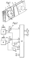
- a coin passageway 2 includes a ramp 4 which is inclined in a first plane to the horizontal so that a coin such as that indicated at 6 will slide or roll in the direction of arrow A down the ramp.
- the ramp is also inclined to the horizontal in a perpendicular plane, so that the coins will tend to move with their faces in contact with one side wall 8 of the passageway, which thus acts as a reference plane.
- the validator also has a pair of inductance sensors formed by coils 10 and 12.
- the coil 10 is positioned adjacent to and just behind the reference plane formed by side wall 8.
- the coil is covered by a membrane (not shown) which is flush with the side wall. This separates the coil from the reference plane by a predetermined distance equal to the thickness of the membrane.
- the coil 12 is similarly mounted on the other side of the passageway, spaced by a respective membrane from the inner surface of a side wall 14 opposed to the side wall 8. Both coils are thus accurately positioned with respect to the side walls, and therefore with respect to the possible range of positions across the coin passageway which can be adopted by a coin.
- each of the coils 10 and 12 is connected into a respective oscillator circuit 16 or 18.
- the validator has a microprocessor 20 (e.g. salected from the Motorola 6805 family) which has input/output lines 01 to 011, and a timer/counter input terminal T1.
- a microprocessor 20 e.g. salected from the Motorola 6805 family
- T1 timer/counter input terminal
- the oscillators 16 and 18 can be turned on and off by switches 22 and 24, respectively, which are controlled by the microprocessor output terminals O1 and O2, respectively. When switched on, each oscillator operates at a relatively high frequency, e.g. 1.0 MHz. The frequencies are preferably high, so that the fields do not substantially penetrate the coins and the effects of the coins therefore are not substantially influenced by their material composition. Outputs carrying signals at the sensor frequencies (or scaled versions thereof) appear on lines 26 and 28, respectively. Pulses on these lines can be delivered to the terminal T1 by closing gates 30 and 32, respectively, which gates are under the control of signals appearing on input/output lines 03 and 04, respectively.
- the microprocessor can thus turn on either of the oscillators 16 and 18, and close the respective gates 30 or 32 for a predetermined time period during which sensor output pulses appearing at terminal T1 can be counted by an internal counter of the microprocessor to provide a measure of sensor frequency.
- the microprocessor In the absence of the coin, the microprocessor repeatedly turns on the oscillator 16 for a brief period and checks the output frequency. If successive frequency readings change by a certain amount, it is determined that a coin has started to enter the field generated by the coil 10. In this way, coin arrival is detected and used to power up various other parts of the validator circuitry, in a manner which is known per se. From that time, the microprocessor 20 repeatedly enables and disables the oscillators 16 and 18 in an alternating fashion so as to take successive readings from each sensor. Sensor readings may be taken at regular intervals, or in pairs, with a greater interval between successive pairs than between the individual readings of each pair.
- the microprocessor ceases to power up the oscillator 18, except that one or a few further measurements may be taken from each of the sensors to establish idle values, i.e. frequency measurements in the absence of a coin.
- the sensor values which are used in the deduction of a thickness measurement are derived from the relationship between the sensed frequencies during the passage of the coin and the idle frequencies (e.g. the difference between or ratio of the frequencies). This technique, which is known per se, reduces the effects of drift of circuit component values, temperature changes, etc.
- the idle values can be taken when a further sensor (not shown) detects the presence of a coin, to ensure that the idle values are measured after the coin has completely left the region of the sensors 10 and 12.
- the actual thickness detection operation which takes place while the coin is passing may be based on the idle levels detected following passage of the preceding coin. Obviously, this could be avoided by monitoring the idle values before the coin reaches the sensor, e.g. by alternately switching on the oscillators for very brief periods.
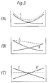
- Figure 3(A) illustrates typical sensor outputs for a coin of given thickness.
- the horizontal axis represents the positioning of the coin across the width of the passageway.
- the vertical axis represents on an arbitrary scale the maximum difference between the sensor output frequency and the idle frequency as the coin passes the sensor.
- Line I represents the output for sensor 10
- line II the output for sensor 12.
- the broken line represents (on a different scale) the combined outputs which would be obtained if the coils were connected in series or in parallel. It will be observed that the combined output varies substantially depending upon coin position.
- Figure 3(B) is similar, but in this case the sensors have been carefully designed so that their responses do not vary substantially from linear responses. Although there is some inaccuracy in the combined measurements due to the slight non-linearity of the responses, there is a greater inaccuracy due to the fact that the gradients of the response curves are different. Although it may be possible by careful designing and positioning of the coils to obtain response curves which are reasonably linear or reasonably symmetrical, achieving both these results for all possible coin positions and thicknesses has not proved possible.
- the microprocessor 20 takes each of the frequency shift measurements from each sensor, and processes it so as to avoid such problems.
- the microprocessor has a read-only memory (not shown) storing a set of processed values, each of which corresponds to a respective sensor output value. The sensor output value is used to determine the address in the table from which the processed value is to be retrieved.
- Figure 3(C) illustrates how the processed values I′ and II′ vary with coin position. It will be observed that the response curves are linear and symmetrical, and therefore when the processed values are combined by the microprocessor 20, the resulting response shown in broken lines in Figure 3(C) is substantially independent of coin position.
- the values stored in the look-up table are preferably determined experimentally, and may be deduced individually for each validator so as to take into account possible tolerance variations and thereby effectively to calibrate each mechanism. If both sensor response curves are substantially non-linear, as in Figure 3(A), it is desirable for both sets of sensor output values to be processed to render them linear. However, if the sensor output responses are substantially linear as shown in Figure 3(B), it may be necessary to process the output of only one sensor in order to scale the output to correspond with that of the other sensor. In any event, the processing should result in substantially linear response curves with substantially the same gradient or constant of proportionality, as shown in Figure 3(C).
- the microprocessor 20 converts each sensor output value to a processed value using the look-up table, and combines pairs of output values from the respective sensors to produce a single combined value which is representative of detected thickness. As the coin enters the region between the sensors, this value will increase to a maximum, then stay at this maximum level as the coin passes the sensors, and then decrease to an idling level as the coin leaves the sensors. The maximum value is taken to be the thickness measurement.
- Figure 4 illustrates how the present embodiment avoids not merely the problems resulting from an indeterminate position of the coin as it passes the sensor, but also problems caused by variations in that position during the period in which it is passing the sensors.
- the graphs (A) to (F) of Figure 4 have vertical axes representing senscr outputs on an arbitrary scale, and horizontal axes representing time. The coin enters the region between the sensors in the period leading up to time t1, fully overlaps the sensors in,the period between t1 and t2, and then after t2 starts to depart from the sensors.
- Figure 4 illustrates the situation where the coin is relatively close to the sensor 12 when it enters the region between the sensors, but is substantially midway between the coils by the time it leaves the region.
- Figure 4A which represents the output of sensor 10
- d the sensor output increases by an amount d.
- Figure 4B which represents the output of the sensor 12
- D the amount of the response curves which make changes in the position of the coin affect the nearest coil greater than they affect the furthest coil.
- Figures 4(D) and 4(E) represent the processed outputs of sensors 10 and 12, respectively. Because these processed outputs are linear, the variation d′ in the period t1 to t2 in the processed output of sensor 10 is equal and opposite to the variation D′ in the processed output of sensor 12. Thus, when the outputs are combined, a horizontal peak value as shown in Figure 4(F) providing an accurate measurement of thickness is obtained. This illustrates that the measurement is unaffected either by coin position or variations in the position.
- the embodiment described above derives measurements by detecting shifts in the frequency of an oscillator.
- the measurements may alternatively be based on absolute frequency values, amplitudes, amplitude shifts, phase shifts, etc.
Landscapes
- Physics & Mathematics (AREA)
- General Physics & Mathematics (AREA)
- Testing Of Coins (AREA)
- Acyclic And Carbocyclic Compounds In Medicinal Compositions (AREA)
- Graft Or Block Polymers (AREA)
- Measurement Of Length, Angles, Or The Like Using Electric Or Magnetic Means (AREA)
- Liquid Crystal (AREA)
- Noodles (AREA)
Claims (9)
- Verfahren zum Prüfen von Münzen auf Dicke unter Benutzung eines Paares von Induktionsgliedern (10, 12), die auf den jeweiligen Seiten (8, 14) eines Münzweges (4) angeordnet sind und deren Ausgänge kombiniert sind, um ein die Dicke anzeigendes Signal zu erzeugen, wobei das genannte Signal im wesentlichen unabhängig ist von der Lage der Münze über mindestens einen begrenzten Lagebereich zwischen den genannten Induktionsgliedern (10, 12) für eine vorgegebene Münzdicke, gekennzeichnet durch die folgenden Schritte:
Erzeugen getrennter Induktionsglied-Ausgangswerte, die jeweils eine Aussage über die Auswirkung einer Münze (6) auf ein elektromagnetisches Feld liefern, ermittelt durch jeweils eines der Induktionsglieder (10, 12), wobei die Gradienten der Abhängigkeiten der genannten Induktionsglied-Ausgangswerte auf die Lage der genannten Münze mit der genannten, vorgegebenen Dicke innerhalb des genannten Lagebereichs unterschiedlich ist, und
Verarbeiten mindestens eines der Induktionsglied-Ausgangswert und Kombinieren der Werte, um das genannte, die Dicke anzeigende Signal zu erzeugen, wobei die Verarbeitung des genannten, mindestens einen Induktionsglied-Ausgangswertes unterschiedlich ist von der des anderen, um im wesentlichen das genannte, die Dicke anzeigende Signal für die genannte Gradientendifferenz zu kompensieren. - Verfahren, wie beansprucht in Anspruch 1, worin die Werte repräsentativ sind für die Münzauswirkungen, die im wesentlichen im selben Augenblick erfaßt wurden.
- Verfahren, wie beansprucht in Anspruch 2, mit dem Schritt des aufeinanderfolgenden Kombinierens von verarbeiteten Werten, und mit dem Erfassen der Spitzen der Ergebnisse, um die die Dicke bezeichnende Messung zu erhalten.
- Verfahren, wie beansprucht in irgendeinem vorangehenden Anspruch, worin die Induktionsglieder (10, 12) so angeordnet sind, daß die hierdurch erzeugten Werte in nicht linearer Zuordnung zur Münzenlage stehen, und worin die Verarbeitung der Werte so ist, daß sie in eine lineare Zuordnung zur Münzenlage umgewandelt werden.
- Verfahren, wie beansprucht in irgendeinem vorangehenden Anspruch, worin die Verarbeitung unter Benutzung einer Nachschlagetabelle erreicht wird, die Ausgangswerte verarbeiteten Werten zuordnet.
- Verfahren, wie beansprucht in jedem vorangehenden Anspruch, mit dem Schritt des Betreibens der Induktionsglieder aufeinanderfolgend, wenn die Münze die Induktionsglieder passiert.
- Verfahren, wie beansprucht in irgendeinem vorangehenden Anspruch, mit dem Schritt der Benutzung eines einzigen der Induktionsglieder, um die Ankunft einer Münze im Münzprüfer zu erfassen, und ferner mit dem Schritt, selektive Abschnitte des Münzprüfers in Abhängigkeit von der genannten Ermittlung unter Strom zu setzen.
- Verfahren nach Anspruch 1, ferner mit den Schritten der Digitalisierung der genannten Induktionsglied-Ausgangswerte und der Verarbeitung der genannten Induktionsglied-Ausgangswerte unter Verwendung gespeicherter Daten, die eine Verarbeitung zum Ausgleich der Abhängigkeit der genannten Induktionsglied-Ausgangswertverteilungen von dem genannten, die Dicke anzeigenden Signal für eine Vielzahl von Lagen zwischen den Induktionsgliedern festlegen.
- Münzprüfer, der betreibbar ist, um die Münzdicke zu messen, unter Verwendung eines Verfahrens, wie beansprucht in irgendeinem vorangehenden Anspruch.
Applications Claiming Priority (3)
| Application Number | Priority Date | Filing Date | Title |
|---|---|---|---|
| GB8917258 | 1989-07-28 | ||
| GB8917258A GB2234619B (en) | 1989-07-28 | 1989-07-28 | Coin validators |
| PCT/GB1990/001168 WO1991002334A1 (en) | 1989-07-28 | 1990-07-27 | Coin validators |
Publications (2)
| Publication Number | Publication Date |
|---|---|
| EP0484441A1 EP0484441A1 (de) | 1992-05-13 |
| EP0484441B1 true EP0484441B1 (de) | 1995-03-22 |
Family
ID=10660761
Family Applications (1)
| Application Number | Title | Priority Date | Filing Date |
|---|---|---|---|
| EP90912332A Expired - Lifetime EP0484441B1 (de) | 1989-07-28 | 1990-07-27 | Münzprüfer |
Country Status (15)
| Country | Link |
|---|---|
| US (1) | US5337877A (de) |
| EP (1) | EP0484441B1 (de) |
| JP (1) | JP2972332B2 (de) |
| KR (1) | KR920704242A (de) |
| AT (1) | ATE120295T1 (de) |
| AU (1) | AU647700B2 (de) |
| BR (1) | BR9007564A (de) |
| CA (1) | CA2063738C (de) |
| DD (1) | DD296770A5 (de) |
| DE (1) | DE69018081T2 (de) |
| ES (1) | ES2069743T3 (de) |
| GB (1) | GB2234619B (de) |
| HU (1) | HU9200261D0 (de) |
| IE (1) | IE902515A1 (de) |
| WO (1) | WO1991002334A1 (de) |
Families Citing this family (11)
| Publication number | Priority date | Publication date | Assignee | Title |
|---|---|---|---|---|
| AU688449B2 (en) * | 1994-03-28 | 1998-03-12 | Abey Australia Pty Ltd | Improved heavy duty brick tie |
| US5626262A (en) * | 1995-06-07 | 1997-05-06 | Redmond Products, Inc. | Dispensing container with drainage passages |
| US5655687A (en) * | 1995-06-07 | 1997-08-12 | Redmond Products, Inc. | Base end dispensing container with travel cap |
| WO1997035286A1 (de) * | 1996-03-19 | 1997-09-25 | Electrowatt Technology Innovation Ag | Anordnung zum prüfen von münzen |
| GB2323200B (en) | 1997-02-24 | 2001-02-28 | Mars Inc | Coin validator |
| US5992603A (en) * | 1997-12-18 | 1999-11-30 | Ginsan Industries Inc | Coin acceptance mechanism and method of determining an acceptable coin |
| GB2340681B (en) | 1998-08-14 | 2003-07-30 | Mars Inc | Oscillators |
| US6230870B1 (en) * | 2000-02-10 | 2001-05-15 | Coin Acceptors, Inc. | Coin detection device |
| ES2170678B1 (es) | 2000-06-30 | 2003-09-16 | Azkoyen Medios De Pago Sa | Metodo y aparato de obtencion de caracteristicas fisicas de monedas para su identificacion. |
| JP4022583B2 (ja) * | 2002-03-11 | 2007-12-19 | 旭精工株式会社 | コインセレクタ |
| CN104134269B (zh) * | 2014-06-23 | 2017-07-07 | 江苏多维科技有限公司 | 一种硬币检测系统 |
Family Cites Families (12)
| Publication number | Priority date | Publication date | Assignee | Title |
|---|---|---|---|---|
| DE2646025A1 (de) * | 1976-10-12 | 1978-04-13 | Siemens Ag | Elektronische muenzpruefung mit mathematisch definierten annahmebereichen |
| JPS5724803A (en) * | 1980-07-22 | 1982-02-09 | Yoshitsuka Seiki:Kk | Measuring device for size of powder-molded, press-molded product |
| EP0146251B1 (de) * | 1983-11-04 | 1992-08-12 | Mars Incorporated | Vorrichtung zum Erkennen der Gültigkeit von Münzen |
| JPS60262292A (ja) * | 1984-06-08 | 1985-12-25 | 株式会社田村電機製作所 | 硬貨検査装置 |
| US4678994A (en) * | 1984-06-27 | 1987-07-07 | Digital Products Corporation | Methods and apparatus employing apparent resonant properties of thin conducting materials |
| GB8510181D0 (en) * | 1985-04-22 | 1985-05-30 | Aeronautical General Instr | Moving coin validation |
| CH667546A5 (de) * | 1985-07-26 | 1988-10-14 | Autelca Ag | Einrichtung zur muenzenpruefung. |
| JPS62164190A (ja) * | 1986-01-16 | 1987-07-20 | 三洋電機株式会社 | 硬貨識別装置 |
| GB2207270B (en) * | 1987-07-20 | 1991-06-19 | Thomas Patrick Sorensen | Improvements in and relating to determining the characteristics of conducting objects |
| JP2567654B2 (ja) * | 1988-03-31 | 1996-12-25 | 株式会社 日本コンラックス | 硬貨選別方法および装置 |
| JPH0786939B2 (ja) * | 1988-05-27 | 1995-09-20 | 株式会社日本コンラックス | 硬貨識別装置 |
| GB8912522D0 (en) * | 1989-05-26 | 1989-07-19 | Coin Controls | Coin discrimination apparatus with temperature compensation |
-
1989
- 1989-07-28 GB GB8917258A patent/GB2234619B/en not_active Expired - Fee Related
-
1990
- 1990-07-10 IE IE251590A patent/IE902515A1/en unknown
- 1990-07-27 DD DD90343116A patent/DD296770A5/de not_active IP Right Cessation
- 1990-07-27 DE DE69018081T patent/DE69018081T2/de not_active Expired - Fee Related
- 1990-07-27 ES ES90912332T patent/ES2069743T3/es not_active Expired - Lifetime
- 1990-07-27 EP EP90912332A patent/EP0484441B1/de not_active Expired - Lifetime
- 1990-07-27 AT AT90912332T patent/ATE120295T1/de active
- 1990-07-27 WO PCT/GB1990/001168 patent/WO1991002334A1/en not_active Ceased
- 1990-07-27 HU HU92261A patent/HU9200261D0/hu unknown
- 1990-07-27 JP JP2511376A patent/JP2972332B2/ja not_active Expired - Fee Related
- 1990-07-27 KR KR1019920700183A patent/KR920704242A/ko not_active Ceased
- 1990-07-27 BR BR909007564A patent/BR9007564A/pt unknown
- 1990-07-27 CA CA002063738A patent/CA2063738C/en not_active Expired - Fee Related
- 1990-07-27 AU AU61894/90A patent/AU647700B2/en not_active Ceased
-
1992
- 1992-07-31 US US07/923,860 patent/US5337877A/en not_active Expired - Lifetime
Also Published As
| Publication number | Publication date |
|---|---|
| WO1991002334A1 (en) | 1991-02-21 |
| GB2234619A (en) | 1991-02-06 |
| IE902515A1 (en) | 1991-02-13 |
| GB2234619B (en) | 1993-04-14 |
| HU9200261D0 (en) | 1992-04-28 |
| GB8917258D0 (en) | 1989-09-13 |
| ES2069743T3 (es) | 1995-05-16 |
| DE69018081D1 (de) | 1995-04-27 |
| AU6189490A (en) | 1991-03-11 |
| JP2972332B2 (ja) | 1999-11-08 |
| JPH04507020A (ja) | 1992-12-03 |
| BR9007564A (pt) | 1992-06-30 |
| CA2063738A1 (en) | 1991-01-29 |
| EP0484441A1 (de) | 1992-05-13 |
| DE69018081T2 (de) | 1995-10-19 |
| AU647700B2 (en) | 1994-03-24 |
| KR920704242A (ko) | 1992-12-19 |
| US5337877A (en) | 1994-08-16 |
| DD296770A5 (de) | 1991-12-12 |
| HK1007024A1 (en) | 1999-03-26 |
| CA2063738C (en) | 2000-07-18 |
| ATE120295T1 (de) | 1995-04-15 |
Similar Documents
| Publication | Publication Date | Title |
|---|---|---|
| AU647700B2 (en) | Coin validators | |
| US5213190A (en) | Method and apparatus for testing coins | |
| JPH0731324Y2 (ja) | 硬貨判別装置 | |
| GB2151062A (en) | Coin validator | |
| EP1012796B1 (de) | Verfahren und vorrichtung zum überprüfen von münzen | |
| HK1007024B (en) | Coin validators | |
| EP0527874B1 (de) | Verfahren und vorrichtung zum prüfen von münzen | |
| US6739444B2 (en) | Inductive coin sensor with position correction | |
| EP0359470B1 (de) | Prüfen von durchlaufenden Münzen | |
| JPS6211760B2 (de) | ||
| JPS623396A (ja) | 硬貨判別処理方式 | |
| US6076651A (en) | Coin diameter measurement | |
| WO1993021608A1 (en) | Method and apparatus for testing coins | |
| JPH06111094A (ja) | 硬貨検査機 | |
| KR920005340B1 (ko) | 자동판매기의 경화 선별 장치 | |
| JPS6236592B2 (de) | ||
| JPH0797424B2 (ja) | 硬貨選別装置 | |
| JPH0654510B2 (ja) | 硬貨判別装置 | |
| JPS6058514B2 (ja) | 硬貨選別装置 | |
| JPH07118031B2 (ja) | 硬貨判別装置 | |
| JPH06231334A (ja) | 硬貨選別処理装置における硬貨通路開放検知装置 |
Legal Events
| Date | Code | Title | Description |
|---|---|---|---|
| PUAI | Public reference made under article 153(3) epc to a published international application that has entered the european phase |
Free format text: ORIGINAL CODE: 0009012 |
|
| 17P | Request for examination filed |
Effective date: 19920221 |
|
| AK | Designated contracting states |
Kind code of ref document: A1 Designated state(s): AT BE CH DE DK ES FR GB IT LI LU NL SE |
|
| 17Q | First examination report despatched |
Effective date: 19940518 |
|
| GRAA | (expected) grant |
Free format text: ORIGINAL CODE: 0009210 |
|
| AK | Designated contracting states |
Kind code of ref document: B1 Designated state(s): AT BE CH DE DK ES FR GB IT LI LU NL SE |
|
| PG25 | Lapsed in a contracting state [announced via postgrant information from national office to epo] |
Ref country code: BE Effective date: 19950322 Ref country code: NL Free format text: LAPSE BECAUSE OF NON-PAYMENT OF DUE FEES Effective date: 19950322 Ref country code: AT Effective date: 19950322 Ref country code: DK Effective date: 19950322 |
|
| REF | Corresponds to: |
Ref document number: 120295 Country of ref document: AT Date of ref document: 19950415 Kind code of ref document: T |
|
| REF | Corresponds to: |
Ref document number: 69018081 Country of ref document: DE Date of ref document: 19950427 |
|
| REG | Reference to a national code |
Ref country code: ES Ref legal event code: FG2A Ref document number: 2069743 Country of ref document: ES Kind code of ref document: T3 |
|
| ITF | It: translation for a ep patent filed | ||
| ET | Fr: translation filed | ||
| PG25 | Lapsed in a contracting state [announced via postgrant information from national office to epo] |
Ref country code: SE Effective date: 19950622 |
|
| PG25 | Lapsed in a contracting state [announced via postgrant information from national office to epo] |
Ref country code: LU Free format text: LAPSE BECAUSE OF NON-PAYMENT OF DUE FEES Effective date: 19950731 |
|
| NLV1 | Nl: lapsed or annulled due to failure to fulfill the requirements of art. 29p and 29m of the patents act | ||
| PLBE | No opposition filed within time limit |
Free format text: ORIGINAL CODE: 0009261 |
|
| STAA | Information on the status of an ep patent application or granted ep patent |
Free format text: STATUS: NO OPPOSITION FILED WITHIN TIME LIMIT |
|
| 26N | No opposition filed | ||
| REG | Reference to a national code |
Ref country code: GB Ref legal event code: IF02 |
|
| PGFP | Annual fee paid to national office [announced via postgrant information from national office to epo] |
Ref country code: CH Payment date: 20030730 Year of fee payment: 14 |
|
| PG25 | Lapsed in a contracting state [announced via postgrant information from national office to epo] |
Ref country code: LI Free format text: LAPSE BECAUSE OF NON-PAYMENT OF DUE FEES Effective date: 20040731 Ref country code: CH Free format text: LAPSE BECAUSE OF NON-PAYMENT OF DUE FEES Effective date: 20040731 |
|
| REG | Reference to a national code |
Ref country code: CH Ref legal event code: PL |
|
| REG | Reference to a national code |
Ref country code: GB Ref legal event code: 732E |
|
| REG | Reference to a national code |
Ref country code: FR Ref legal event code: TP |
|
| REG | Reference to a national code |
Ref country code: GB Ref legal event code: 732E |
|
| REG | Reference to a national code |
Ref country code: FR Ref legal event code: GC |
|
| PGFP | Annual fee paid to national office [announced via postgrant information from national office to epo] |
Ref country code: FR Payment date: 20070710 Year of fee payment: 18 |
|
| PGFP | Annual fee paid to national office [announced via postgrant information from national office to epo] |
Ref country code: DE Payment date: 20080807 Year of fee payment: 19 Ref country code: ES Payment date: 20080821 Year of fee payment: 19 |
|
| PGFP | Annual fee paid to national office [announced via postgrant information from national office to epo] |
Ref country code: IT Payment date: 20080730 Year of fee payment: 19 |
|
| PGFP | Annual fee paid to national office [announced via postgrant information from national office to epo] |
Ref country code: GB Payment date: 20080806 Year of fee payment: 19 |
|
| REG | Reference to a national code |
Ref country code: FR Ref legal event code: ST Effective date: 20090331 |
|
| PG25 | Lapsed in a contracting state [announced via postgrant information from national office to epo] |
Ref country code: FR Free format text: LAPSE BECAUSE OF NON-PAYMENT OF DUE FEES Effective date: 20080731 |
|
| GBPC | Gb: european patent ceased through non-payment of renewal fee |
Effective date: 20090727 |
|
| PG25 | Lapsed in a contracting state [announced via postgrant information from national office to epo] |
Ref country code: GB Free format text: LAPSE BECAUSE OF NON-PAYMENT OF DUE FEES Effective date: 20090727 |
|
| PG25 | Lapsed in a contracting state [announced via postgrant information from national office to epo] |
Ref country code: DE Free format text: LAPSE BECAUSE OF NON-PAYMENT OF DUE FEES Effective date: 20100202 |
|
| REG | Reference to a national code |
Ref country code: ES Ref legal event code: FD2A Effective date: 20090728 |
|
| PG25 | Lapsed in a contracting state [announced via postgrant information from national office to epo] |
Ref country code: ES Free format text: LAPSE BECAUSE OF NON-PAYMENT OF DUE FEES Effective date: 20090728 |
|
| PG25 | Lapsed in a contracting state [announced via postgrant information from national office to epo] |
Ref country code: IT Free format text: LAPSE BECAUSE OF NON-PAYMENT OF DUE FEES Effective date: 20090727 |