US5213190A - Method and apparatus for testing coins - Google Patents
Method and apparatus for testing coins Download PDFInfo
- Publication number
- US5213190A US5213190A US07/868,551 US86855192A US5213190A US 5213190 A US5213190 A US 5213190A US 86855192 A US86855192 A US 86855192A US 5213190 A US5213190 A US 5213190A
- Authority
- US
- United States
- Prior art keywords
- coin
- reactance
- inductor
- loss
- signal
- Prior art date
- Legal status (The legal status is an assumption and is not a legal conclusion. Google has not performed a legal analysis and makes no representation as to the accuracy of the status listed.)
- Expired - Lifetime
Links
Images


Classifications
-
- G—PHYSICS
- G07—CHECKING-DEVICES
- G07D—HANDLING OF COINS OR VALUABLE PAPERS, e.g. TESTING, SORTING BY DENOMINATIONS, COUNTING, DISPENSING, CHANGING OR DEPOSITING
- G07D5/00—Testing specially adapted to determine the identity or genuineness of coins, e.g. for segregating coins which are unacceptable or alien to a currency
- G07D5/08—Testing the magnetic or electric properties
Definitions
- This invention relates to a method and apparatus for testing coins.
- coin is used to encompass genuine coins, tokens, counterfeit coins and any other objects which may be used in an attempt to operate coin-operated equipment.
- Coin testing apparatus in which a coin is subjected to a test by passing it through a passageway in which it enters an oscillating magnetic field produced by an inductor and measuring the degree of interaction between the coin and the field, the resulting measurement being dependent upon one or more characteristics of the coin and being compared with a reference value, or each of a set of reference values, corresponding to the measurement obtained from one or more denominations of acceptable coins. It is most usual to apply more than one such test, the respective tests being responsive to respective different coin characteristics, and to judge the tested coin acceptable only if all the test results are appropriate to a single, acceptable, denomination of coin. An example of such apparatus is described in GB-A-2 093 620.
- At least one of the tests is sensitive primarily to the material of which the coin is made and, in particular, such a test may be influenced by the electrical conductivity, and in magnetic materials the magnetic permeability, of the coin material.
- Such tests have been carried out by arranging for the coin to pass across the face of an inductor, and hence through its oscillating field, and measuring the effect that the coin has, by virtue of its proximity to the inductor, upon the frequency or amplitude of an oscillator of which the inductor forms part. Most often it has been the peak value of the effect, achieved when the coin is central relative to the inductor, that has been measured.
- measurements of this type are sensitive to the distance between the coin and the inductor, in the direction perpendicular to the face of the inductor, at the time when the measurement is made.
- This undesirable effect can be countered to some extent by arranging the mechanical design of the mechanism such that coins are always encouraged to pass the inductor at a fixed distance from it but this can never be achieved completely and requires design features which in other respects may be undesirable.
- the measurement scatter caused by variable coin lateral position may be allowed for by setting the coin acceptance limits wider, so that acceptable coins will always pass the test even though they pass the inductor at different distances from it, but this adversely affects the reliability of the mechanism in rejecting unacceptable coins.
- An object of the invention is to provide a method of testing a coin which is responsive to the material of the coin, and is relatively insensitive to the distance of the coin from a testing inductor.
- the invention provides from one aspect a method of testing a coin in a coin testing mechanism, comprising subjecting a coin inserted into the mechanism to an oscillating field generated by an inductor, measuring the reactance and the loss of the inductor when the coin is in the field, and determining whether the direction in the impedance plane of a displacement line, representing the displacement of a coin-present point defined by the measurements relative to a coin-absent point representing the inductor reactance and loss in the absence of a coin, corresponds to a reference direction in the impedance plane.
- the "impedance plane” as referred to above is a plane in which the reactance (reactive impedance) and the loss (resistive impedance) of a circuit or of an inductor are represented as measurements or vectors along two mutually perpendicular axes lying in that plane.
- the term “displacement line” will be explained later in relation to FIG. 1.
- the invention can be carried out using only a single inductor because the direction of the displacement line is substantially independent of the lateral position of the coin. This simplifies the electrical wiring required and, in a typical coin mechanism where the coin passgeway lies between a body and an openable lid, avoids the need to provide flexible wiring leading to an inductor mounted on the lid.
- the reference direction in the impedance plane is established as an angle relative to one of the reactance and loss axes.
- the position of the coin-absent point in the impedance plane may not be constant, because the reactance of the coil itself, and the loss of the coil itself, may vary with temperature and consequently with time and also small changes in the geometry of the coin mechanism might occur.
- the reactance and the loss of the inductor are measured both when the coin is in the field, and when it is not.
- the direction of the displacement line is determined by the two points in respect of which the measurements have been taken.
- the two reactance measurements are subtracted, the two loss measurements are subtracted, and the ratio of the two differences is taken, this representing the tangent of an angle the displacement line makes with one of the axes.
- the tangent can then be compared with the reference direction which may be established or stored also as the tangent of the corresponding angle for an acceptable coin, represented, of course, as a number in digital form when digital processing and storage are being used for implementation.
- the reference information may constitute for example a set of stored coordinates in the impedance plane which together define a reference displacement line the direction of which is the reference direction and the position of which is such that it extends through the substantially fixed coin-absent point. Then, the determination of whether the direction of the displacement line corresponds to the reference direction need not involve actually measuring the coin-absent point. It can be assumed that that point has not changed, so the correspondence of the two directions, or otherwise, can be determined simply by checking whether the coin-present point lies on the reference displacement line. If it does, then the coin will have caused displacement of the coin-present point in the direction of the reference displacement line.
- the reference direction is established as an angle relative to the coin-absent total impedance vector of the inductor, instead of relative to the loss or reactance axes. This is of particular value, as will be explained below, when the reactance and loss measurements are taken by a phase discrimination method.
- Using a phase discrimination method has advantages, which are mentioned above, but also can introduce errors due to reference signals employed not being accurately phased. Measuring the direction of displacement of the impedance plane point caused by the coin relative to the total impedance vector of the inductor and establishing the reference direction also as an angle relative to that total impedance vector reduces or eliminates such errors.
- phase discrimination method has the advantages already mentioned, but also can introduce errors due to reference signals employed not being accurately phased.
- the direction of the displacement line is computed from signal ratios. Because ratios are taken, the result is independent of the gain of the channel which handles the relevant signals. However, when it is also desired to use as an acceptability criterion the difference between the coin-present and the coin-absent reactance, then the gain of the channel becomes important.
- a further feature of the invention usable irrespective of whether the measurements are taken using a phase discrimination technique, or not, comprises compensating for the effect of varying system gain on said difference between reactance values by simulating, from time to time, a predetermined change in the reactance of the inductor when a coin is not in its field, detecting the resulting change in a signal dependent on said reactance which signal has been subjected to said system gain, comparing the detected change with a reference value, applying to said reactance-dependent signal a compensation factor derived from the result of said comparison such as to adjust that signal to substantially correspond with the reference value, and maintaining the application of said compensation factor until the next time said change is simulated.
- the invention provides a method of testing a coin in a coin testing mechanism, comprising subjecting a coin inserted into the mechanism to an oscillating field generated by an inductor, measuring the reactance and the loss of the inductor when the coin is in the field, and determining whether the direction in the impedance plane of a displacement line, representing the displacement of a coin-present point defined by the measurements relative to a coin-absent point representing the inductor reactance and loss in the absence of a coin, corresponds to a reference direction in the impedance plane, and wherein the frequency of the oscillating field generated by the inductor is sufficiently low that its skin depth for the coin material is greater than the thickness of the coin, whereby the direction of said displacement line is influenced by the thickness of the coin being tested.
- a further aspect of the invention is a coin testing mechanism for carrying out methods in accordance with the invention as referred to above.
- FIG. 1 represents the impedance plane for the inductor of the coin testing apparatus shown in FIG. 2,
- FIG. 2 shows schematically a circuit for developing the X and R signals, using a phase discrimination method
- FIG. 3 is a further impedance plane diagram useful in explaining operation of the circuit of FIG. 2,
- FIG. 4 shows how X and R vary with time as a coin passes the inductor
- FIG. 5 shows how an angle ⁇ varies with time as a coin passes the inductor
- FIG. 6 is a further impedance plane diagram useful in explaining a further developed method of testing coins in accordance with the invention.
- FIG. 7 illustrates a substantial part of a circuit similar to that of FIG. 2 but including additional features
- FIG. 8 is a further impedance plane diagram useful in understanding the functioning of the circuit of FIG. 7,
- FIG. 9 is a further impedance plane diagram useful in understanding the effect of offsets which are applied within the circuit of FIG. 7,
- FIG. 10 is a graph showing how an angle ⁇ measured in the impedance plane varies with thickness and with frequency when measurements are taken on test discs of the same material but of different thicknesses,
- FIG. 11 shows schematically a further coin testing apparatus utilising the invention, in which the X and R signals are developed using a free running oscillator instead of a driven coil, and
- FIG. 12 illustrates the relationship between frequency, phase and effective resistance in the tuned circuit of FIG. 11.
- the vertical axis represents the imaginary component, i.e. the reactance X, of the impedance of an inductor such as the coil 104 of the apparatus shown in FIG. 2, as affected by any coin which may be near it.
- the horizontal axis represents the real component of the impedance i.e. its resistance or loss R, again as affected by any coin which may near the coil.
- both the effective reactance and the effective loss of the coil will change, that is to say that if X and R are now measured for coil plus coin the resulting values will define a different point b in the impedance plane.
- the position of the line a-b may move in the impedance plane, for example to the parallel position a'-b', but its gradient, the angle ⁇ , remains the same for the same type of coin. That is to say, the direction of the line on which the point representing the coin/coil combination in the impedance plane has moved relative to the coil-only point (herein called the "displacement line”) is indicative of coin type and substantially independent of the lateral position of the coin.
- the loss is increased by the additional factor of hysteresis loss, and the reactance may increase instead of decreasing, since the coin will, to a degree, act as a core for the coil.
- the angle ⁇ will be in the opposite sense from that shown in FIG. 1. This may be used to discriminate between magnetic and non-magnetic coins.
- values of X and R are measured when no coin is present, and then when a coin is adjacent to the coil, the X values are subtracted and the R values are subtracted so as to give ⁇ X and ⁇ R as indicated in FIG. 1, these values indicating by how much the coin has changed the effective reactance and the effective loss of the coil, and ⁇ X/ ⁇ R is taken; this is tan ⁇ for the unknown coin. Acceptability is tested by comparing this with a reference value of tan ⁇ which corresponds to the ratio of the measured values of ⁇ X and ⁇ R for an acceptable coin.
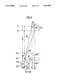
- Means for positioning a coin shown in broken lines at 10 adjacent to a coil 104, the means being shown schematically as a coin passageway 12 along which the coin moves on edge past the coil.
- a practical arrangement for passing a moving coin adjacent to an inductive testing coil is shown, for example, in GB-A-2 093 620.
- the apparatus utilises the peak values.
- the circuit of FIG. 2 uses a phase discrimination technique for separating the real (R) and imaginary (X) components of the coil impedance. It comprises a signal source consisting of a digital frequency generator 100 whose output is filtered by a filter 102 whose output controls a constant current source 103 whose output drives the coin sensing coil 104. Thus, components 100, 102, 103 appear to the coil as a constant current source.
- the output of generator 100 approximates to a sine wave but, being generated digitally, it contains higher harmonics and the function of the filter 102 is to filter these out.
- the signal across coil 104 is applied to a phase sensitive detector 106 which also receives, from the generator 100, two reference signals.
- One reference signal is on line 108 and ideally is in phase with the voltage across coil 104 so as to enable the phase sensitive detector to produce the signal representing X at one of its outputs.
- On another line 110 a reference signal is applied which is at 90° to the first reference signal and in phase with the coil current, so as to enable the phase sensitive detector to develop at another output thereof a signal indicative of R of the coil.
- the voltage signals applied to and output from the phase sensitive detector can only be relied on as measures of X and R so long as the peak coil current is constant with time.
- the R and X signals are filtered by respective filters 112 and 114 and the resulting signals are applied to a microprocessor 116 which is programmed to carry out the necessary further processing of the signals, and also to carry out the further functions required for coin validation. Additionally, microprocessor 116 controls signal generator 100 so that it will generate alternately the reference signals on lines 108 and 110, and also switches the output of the phase sensitive detector 106 between the R and X output channels in synchronism with the switching of the reference signals.
- vector 118 represents the total impedance of coil 104 when no coin is present and hence its end corresponds to point a in FIG. 1.
- vector 118 has been shifted along displacement line 120 to become vector 118'.
- the end of vector 118' corresponds to point b c or d in FIG. 1.
- Microprocessor 116 receives from the phase sensitive detector 106 signals representing the X and R components of both of those vectors and hence can compute ⁇ X and ⁇ R and their ratio ⁇ X/ ⁇ R which is tan ⁇ as referred to before.
- the inductor is shown as a single coil, it may have other configurations, such as a pair of coils opposed across the coin passageway and connected in parallel or series, aiding or opposing.
- FIG. 4 shows how, for a single coin, X and R (both measured in ohms) vary with time as a coin passes the coil. ⁇ X and ⁇ R are also shown. It can be seen that whereas X reaches a relatively smooth and flat negative peak during the middle part of the passage of the coin, R has a relatively smooth plateau in the central part of its peak, with a small further superimposed peak at each end of the plateau, these small peaks being caused by edge effects as the rim of the coin passes the centre of the coil.
- the locus of the point defined by the X and R values in the impedance plane as the coin passes the coil is shown by the hook-shaped curve in FIG. 5.
- the vector 120 from the coin-absent point to the point defined by the present X-R measurements of the moving coin lengthens and rotates clockwise until it reaches the tip of the hook and then performs the reverse movement.
- computations may be carried out by storing the variable values of ⁇ X and ⁇ R occurring throughout the passage of the coin, computing the corresponding time-varying values of ⁇ X/ ⁇ R (i.e. tan ⁇ ) and then detecting the maximum of the computed value of tan ⁇ , this maximum being compared with the reference value of tan ⁇ for an acceptable coin.
- the phase discrimination method of FIG. 2 could be rendered less accurate than is ideally desirable, if the phases of the reference signals on lines 108 and 110 (which define the phase discrimination axes) are, or become, incorrectly related to the phase of the current in coil 104 (which defines the true R and X axes).
- phase error is that the components of the total impedance vectors 118 and 118' in FIG. 3 would be measured relative to discrimination axes X d and R d which are rotated relative to the true reactance and loss axes.
- the calculated value ⁇ X d becomes larger than the desired true value ⁇ X while the calculated value ⁇ R d becomes smaller than the desired true value ⁇ R.
- Measurements taken relative to the discrimination axes X d and R d can be used to derive the angle C, as follows. It is to be noted that angle C is equal to the sum of angles A and B as indicated in FIG. 6. FIG. 6 indicates that R d /X d is the tangent of angle B so that angle B can be computed from those measured values. Also, the tangent of angle A is ⁇ R d / ⁇ X d , so that angle A can be computed from those difference values. Angle C is arrived at by summing the computed angles A and B.
- FIG. 7 shows various additions to the basic phase discrimination measurement type of circuit as shown in FIG. 2.
- components corresponding to those already described with reference to FIG. 2 have been given the same reference numerals as in FIG. 2 and will not be described again.
- the constant current source is in the form of a transistor 103 and associated components.
- the additional components as compared with FIG. 2 are a calibration and offset circuit generally indicated at 130, a pre-amplifier 132 for amplifying the X and R signals, which are taken from the lower end of coil 104, prior to their application to the phase sensitive detector 106, a second offset circuit 134, and a digital-to-analogue converter 136 for converting the outputs of the filters 112 and 114 to digital form for handling by the microprocessor 116.
- a single filter or integrator 112/114 is shown in FIG. 7, this being equivalent to the two separately shown circuits 112 and 114 in FIG. 2. In practice, it would be preferred to use a microprocessor which actually incorporates the analogue-to-digital converter 136.
- phase sensitive detector 106 separates the X signal from the R signal by developing at its output the X signal when the in-phase (with the coil voltage) reference signal is being applied on line 108, and the R signal when the quadrature-phase reference signal is being applied on line 110. Consequently, the circuit components from the output of phase sensitive detector 106 to microprocessor 116 are serving as a common channel for the X and R signals but at any one moment are handling only one or the other of them.
- a first significant function of the FIG. 7 circuitry is to provide an alternative manner of dealing with the problem caused by angular displacement of the phase discrimination axes relative to the true X and R axes; that is to say, alternative to the method previously described with reference to FIGS. 3 and 6 in which the angle C between the displacement line 120 and the total impedance vector 118 was calculated instead of the error-influenced angle ⁇ d .
- the first step is to measure the phase-error angle ⁇ c (see FIG. 3) in a way which will be described below. It can be seen from FIG. 3 that ⁇ c is the difference between the desired angle ⁇ and the erroneous angle ⁇ d .
- ⁇ c is the difference between the desired angle ⁇ and the erroneous angle ⁇ d .
- the microprocessor 116 can adjust the digital generator 100 such that the phases of the reference signals on both lines 108 and 110 are shifted in a direction tending to reduce ⁇ c to zero. This will usually not be possible because, since generator 100 is digital, the phases of its outputs can only be adjusted in steps and so normally there will be a residual value of ⁇ c which cannot be eliminated by adjustment.
- the principle is to simulate, by operation of the calibration and offset circuit 130, a change in the reactance in the coil 104 when there is no coin in its field. It can be appreciated from a study of FIG. 3 that if the phase-error angle ⁇ c were 0, and the X component of the coil impedance vector 118 were changed without changing its R component, then there would not be any change either in the R component as perceived or measured at the output of the phase sensitive detector 106. However, if the phase-error angle ⁇ c is not 0, so that in FIG. 3 axis R d does not coincide with axis R, there will be a change in the R value as measured along the axis R d .
- FIG. 8 shows how, when a simulated change ⁇ X d is imposed on the X-component of the total impedance vector 118, converting it to vector 118", there is no change in its R component as measured along the true R axis.
- ⁇ c the phase discrimination axes X d and R d are in error by an angle ⁇ c as before, it can be seen that as measured on axis R d , there is a change ⁇ R d in the measured R value.
- ⁇ R d / ⁇ X d is the tangent of angle ⁇ c .
- the calibration and offset circuit 130 in FIG. 7 simulates the change in the coil impedance X component, and makes sure that the simulation does not affect the coil R component, and then the relationship between the change in R as measured from the output of phase sensitive detector 106, and the change in the X measurement, is used as a basis for computing the error angle ⁇ c .
- calibration and offset circuit 130 The normal operating configuration of calibration and offset circuit 130 is with transistor T2 switched off and transistor T1 switched on.
- the current in coil 104 is then split between series resistors Rb and Rc on the one hand and the parallel resistor Ra on the other hand. These are all precision resistors. It needs to be remembered that in the FIG. 7 circuit it is that voltage component across coil 104 which is in phase with the current through coil 104 that is being taken as a measure of the coil loss R. This is only a true representation so long as the magnitude of the coil current remains constant. It is the value of the voltage component across coil 104 that is 90° out of phase with the coil current that is being taken as a measure of coil reactance X.
- this latter voltage has an offset applied to it for a reason which will be described later, by tapping between resistors Rb and Rc to obtain a voltage which is in phase with the coil current, changing the phase of that tapped-off voltage by 90° by means of capacitor Ci, and applying the resulting phase-shifted voltage to the input of the pre-amplifier 132.
- This offset voltage is 180° out of phase with the imaginary, or reactance-related, component of the voltage across coil 104 and so the effect is simply to apply a fixed offset to the voltage component which, at the input of pre-amplifier 132, represents the coil reactance X.
- This offset voltage is A.C. and it is phased such that it will not in itself affect the loss-related component of the input voltage to pre-amplifier 132.
- transistor T2 is switched on which introduces precision resistor Rd in parallel with resistor Rc, thus reducing the tapped-off voltage being fed through capacitor Ci.
- This voltage reduction simulates, at the input of pre-amplifier 132 a reduction in the reactance X of coil 104, i.e. ⁇ X d of FIG. 8.
- resistor Ra is switched out by turning off transistor T1.
- the value of resistor Ra is chosen to then keep the coil current constant and so the simulation of the change in X is arranged not, in itself, to also simulate any change in coil loss R, i.e.
- microprocessor 116 Having calculated ⁇ c or at least tan ⁇ c , as ⁇ R d / ⁇ X d , if the resultant angle is greater than the minimum adjustment that can be applied to the digital generator 100, microprocessor 116 instructs the digital generator 100 to make that adjustment, in a sense which reduces the phase discrimination error. At such time as the measured error angle becomes less than the minimum adjustment step, microprocessor 116 sums it with the measured value ⁇ d , so as to obtain the desired angle ⁇ for the coin test. It should be appreciated that ⁇ c may be positive or negative so that the summing may either increase or decrease the measured value ⁇ d .
- the circuitry may instead be adapted so as to simulate a change in R without simulating any change in X, and then calculating ⁇ c or tan ⁇ c from the measured value of ⁇ R d and any resulting measured value of ⁇ X d .
- the X and R signals both have to be processed in the common channel of pre-amplifier 132 and phase sensitive detector 106 and with one signal approximately thirty times the size of the other an extremely poor signal-to-noise ratio would be obtained, possibly making any meaningful extraction of a ⁇ R measurement impossible.
- the offset applied to the X signal through capacitor Ci is substantial, so that it renders the X signal at the input of pre-amplifier 132 comparable in size to the R signal.
- greatly improved use is made of the dynamic range of the operational amplifier 132, and the signal-to-noise ratio can be made acceptable.
- the exact value of the offset voltage is not important, so long as it remains constant, because it is applied against both the coin-present and coin-absent X values and hence does not cause any alteration in the difference ⁇ X which is used in computing the angle ⁇ or its tangent. No offset is applied against the R signal at the input of pre-amplifier 132.
- Calibration and offset circuit 130 has a third function but it is necessary, before explaining it, to refer to a further technique used in testing coins, using the circuit of FIG. 7.
- coin diameter is a useful one.
- the direction of the displacement line (for example the angle ⁇ ) is not sufficiently sensitive to coin diameter to provide a useful diameter test, even if the coil is made approximately as large as, or larger than, the largest-diameter coin to be tested. It is found that, when using the circuit of FIG. 7, and so long as the diameter of the inductor 104 is about as large as or larger than the diameter of the largest coin to be tested, the value of ⁇ X is usefully sensitive to coin diameter, and can be used as a second coin test, the coin only being accepted when its ⁇ X value corresponds to that of the same type of acceptable coin as does its displacement line direction.
- the value of the ⁇ X signal alone will be dependent upon the system gain, and this can be expected to vary with time and with temperature.
- the calibration and offset circuit 130 is periodically (for example on switching on, and every few minutes) operated as follows.
- transistor T2 is switched off during normal operation of the circuit.
- transistor T1 is also switched off, thus taking resistor Ra out of the circuit. Since this is in parallel with Rb and Rc the total resistance is increased and the current through coil 104 falls. Since the three resistors Ra, Rb and Rc are precision resistors, they can be selected so that switching Ra out will repeatably produce a quite accurately constant percentage change in the coil current, for example 2%. So far as the X-component of the coil voltage is concerned, this will appear as a 2% decrease in the coil reactance.
- the system will be designed to operate with some desirable level of overall gain from the coil 104 to the output of the digital-to-analogue converter 136.
- the desired overall gain is such that a 2% change in the X-component of the coil voltage should produce a count change of 200 at the analogue-to-digital converter output.
- T1 is switched off to cause the 2% change
- the resulting change in counts at the output of the analogue-to-digital converter is checked by the microprocessor 116. If it is 200, no action is taken, but if it is different from 200, say n, then the compensation factor 200/n is calculated.
- transistor T1 is switched on again to return the circuit to its normal operating configuration and subsequently each time ⁇ X is calculated by the microprocessor 116 (based of course upon the count outputs of the analogue-to-digital converter 136 for coin-present and coin-absent X values), the result is multiplied by the compensation factor 200/n thus producing a ⁇ X value which has been compensated for variations in the system gain.
- variations in gain of the analogue components are measured and are then compensated for by multiplication at the digital stage such that constant gain is maintained as between the output from the coil and the final computed ⁇ X value.
- the analogue-to-digital converter 136 forms a further common channel in which both the X and R signals are to be processed.
- the X signal decreases and the R signal increases.
- further offsets are applied to both the X and R signals such that the coin-absent value of each signal lies close to the appropriate end of the dynamic range of the analogue-to-digital converter 136.
- FIG. 9 shows the same coin-present and coin-absent impedance vectors 118 and 118' as FIG. 3 on a more realistic scale with the X component very much larger than the R component.
- the coin-present and coin-absent X values are X 1 and X 2 respectively.
- the coin-present and coin-absent R values are R 1 and R 2 respectively, the two difference values being shown at top-right in FIG. 9, as ⁇ X and ⁇ R. These define the displacement line 120.
- the substantial first X offset voltage which is applied through capacitor Ci as was previously described is represented as Xo and reduces X 1 and X 2 to X 1o and X 2o where they are comparable in magnitude to R 1 and R 2 , so that line 120 is shifted to 120'.
- the second X offset voltage, applied by second offset circuit 134 is represented as Xo' and shifts the voltages X 1o and X 2o to X 1o' and X 2o' respectively, thus shifting lines 120' to 120".
- the R offset voltage from circuit 134 is indicated at Ro' and shifts the voltages R 1 and R 2 to R 1o' and R 2o' respectively, so that line 120" shifts to 120"'. It can be seen from FIG.
- FIG. 10 shows a set of three curves which represent the values of the angle ⁇ for three test discs which are of the same material but which differ in thickness, and the values of ⁇ being shown over a range of frequencies (on a logarithmic scale) at which coil 104 may be driven.
- the thickness-dependence of the angle ⁇ becomes significant when the frequency is reduced to the point where the skin depth of the field in the material is about one third of the thickness of the material. It can be seen from FIG. 10 that when the frequency is high enough for the skin depth to be much less than the thickness of all of the test discs, the thickness-dependence of the angle ⁇ disappears. The higher the conductivity of the material, the less the skin depth at a given frequency. Consequently it is necessary to go to lower frequencies to achieve useful thickness-dependence for the higher conductivity coin materials.
- the US coin set is primarily of relatively high conductivity materials and to achieve thickness sensitivity with that coin set, and with magnetic coins, it is preferred to use a frequency of 10 kHz or less, for example less than 6 kHz.
- a frequency of 10 kHz or less for example less than 6 kHz.
- cupronickel which is common among the UK coin set
- the conductivity is lower and the skin depth greater at a given frequency, so that significant thickness-dependence can be obtained at frequencies below 100 kHz, preferably below 50 kHz and even more preferably below 35 kHz where the effect is greater.
- the angle ⁇ is dependent on coin thickness as well as material, it remains to a very large extent independent of the spacing of the coin from the coil and so a reliable thickness dependent measurement can be made using a single coil located to one side of the coin path.
- a practical coin testing apparatus has been constructed which employs the techniques described herein with reference to FIG. 7 and which employs two testing inductors comparable with the inductor 104. Both inductors were located on the same side of the coin path.
- the first inductor consisting of an annular coil set into a ferrite pot core was 14 mm in diameter and was driven at 8 kHz.
- the second, regarded in the direction of coin travel, was of similar construction but 37.5 mm in diameter and was driven at 115 kHz. The first was smaller in diameter than the smallest coin to be accepted and was set above the coin track so as to always be completely occluded by the coin when the coin was centred relative to the coil.
- this inductor was driven at the relatively low frequency of 8 kHz, the value of angle ⁇ derived using this coil was dependent on both the material and the thickness of the coin.
- the second inductor was of a diameter greater than that of the largest coin to be accepted and was set with its bottom edge level with the coin track. The higher frequency of 115 kHz ensured that the angle ⁇ derived using this inductor would be substantially independent of coin thickness, but the large diameter of the coil rendered the angle ⁇ sensitive to the diameter or area of the coin as well as its material.
- This inductor was positioned downstream on the coin path to allow any bouncing of the coin to cease, which otherwise would influence the diameter-sensitive measurement on the coin. Such bouncing would have less influence on the output of the much smaller thickness-sensitive inductor.
- Both coils were driven by the same digital signal generator 100 and the output signals from both coils were processed, referring to FIG. 7, by the same pre-amplifier 132 and the further components right through to the microprocessor 116.
- Each of the inductors was provided with its own filter 102, drive transistor 103 and calibration and offset circuit 130 and the two groups of these components were switched into and out of the circuitry of FIG. 7, alternately, at the points marked P in FIG. 7 under the control of microprocessor 116 which simultaneously switched generator 100 between the higher and the lower frequencies appropriate to the two inductors.
- measurements are made when the displacement line direction, and ⁇ X itself, are at extremes, but it is also possible to use measurements taken at other times during the passage of a coin past a sensor, as is known, and the technique described may be used in that way also.
- phase discrimination method is used to derive X, R, ⁇ X and ⁇ R
- various novel and inventive aspects of those embodiments are usable even if alternative methods (such as will be described with reference to FIGS. 11 and 12) are used for those derivations, such as using ⁇ X as an acceptability criterion in addition to displacement line direction, and using displacement line direction at lower frequencies as a thickness-responsive measurement.
- the described technique for compensating for gain variations is usable in coin mechanisms irrespective of the origin or significance of the signals being processed.
- a pi-configuration tuned circuit 2 includes an inductor in the form of a single coil 4, two capacitors 6 and 7 and a resistor 8.
- Resistor 8 is not normally a separate component and should be regarded as representing the effective loss in the tuned circuit, which will consist primarily of the inherent loss of the coil 4.
- Means for positioning a coin shown in broken lines at 10 adjacent to the coil 4, the means being shown schematically as a coin passageway 12 along which the coin moves on edge past the coil.
- the apparatus is responsive to the peak value of this effective loss.
- the tuned circuit 2 is provided with a feedback path so as to form a free-running oscillator.
- the feedback path is generally indicated at 14 and includes a line 16 which carries the voltage occurring at one point in the tuned circuit, a switching circuit 18, and an inverting amplifier 20 which provides gain in the feedback path.
- a phase delay circuit shown schematically at 24 is alternately switched into the feedback path, or by-passed, depending on the condition of switching circuit 18.
- the phase shift round the feedback path is 180° when the phase delay circuit 24 is not switched into it, and the phase shift across the pi-configuration tuned circuit is then also 180°. In this condition the oscillator runs at its resonant frequency.
- FIG. 12 shows the relationship between frequency of oscillation and amount of phase shift ( ⁇ ) in the feedback path for five different values of total effective loss in the tuned circuit, from a relatively low value R1 to a relatively high value R5.
- the amount of effective loss in the circuit at any particular time can be determined by changing the amount of phase shift in the feedback path from one known value to another (or by a known amount) and measuring the resulting change in frequency.
- the relationship between the phase shift change and the frequency change effectively represents the gradient of one of the curves shown in FIG. 12 and consequently indicates on which curve the circuit is operating and hence what is the present effective loss in the circuit.
- the effective loss is the low value R1; but, if the frequency changes by the larger amount ⁇ fC the effective loss is the higher value R4.
- the frequency of the oscillator is fed on line 26 to a frequency sensing circuit 28.
- a control circuit 30 repeatedly operates switching circuit 18 by a line 32 to switch the phase delay circuit 24 into and out of the oscillator feedback path. Via the same line 32 it also operates a switch 34 in synchronism with switching circuit 18 so that the values of the frequency sensed by sensing circuit 28 are stored in store 36 (this being the frequency value when the phase delay is not present in the oscillator circuit) and store 38 (this being the frequency value when the phase delay is introduced into the oscillator circuit).
- FIG. 11 and the following description may be better understood by reference to the following table of the notation used for various frequencies and frequency differences:
- ⁇ fC peak value of ⁇ f when coin present
- fOC peak value of fO when coin present
- fONC value of fO when coin absent
- a subtracter 40 subtracts fO from f ⁇ to develop ⁇ f and, in the normal condition of a switch 42, this value of ⁇ f is passed to a store 44.
- This normal condition prevails while there is no coin adjacent to coil 4, in which case the effective loss in the tuned circuit is low (say, the low value R1 of FIG. 12) and the frequency difference value being stored at 44 is then ⁇ fNC (indicated in FIG. 12), this value being indicative of the inherent effective loss of the tuned circuit itself at the time when the measurements are being taken.
- a section 46 of control circuit 30 detects the beginning of this change from line 48 and in response changes the condition of switch 42 via line 50, causing the recent idling value of ⁇ fNC to be held in store 44.
- Circuit section 46 is adapted to detect this peak occurring and, in response, it causes switch 42 to direct the value of ⁇ f occurring when the coin is centred, to store 52.
- This frequency shift indicates that the total effective loss in the tuned circuit is now the relatively high value R4 consisting of the effective loss inherent in the circuit plus the effective loss introduced into it by the particular coin which is now centred on the coil 4.
- the effective loss R of the coil is k 1 ⁇ f where k 1 is a constant.
- a value indicative of the effective loss introduced by the coin alone is then derived by circuit 54 which subtracts ⁇ fNC from ⁇ fC and multiplies by the constant k 1 . This is equal to ⁇ R as previously referred to.
- the circuit of FIG. 11 also measures ⁇ X, the amount of reactance introduced by the coin into the tuned circuit 2, as follows.
- the value of fO i.e. oscillation frequency without any imposed phase shift
- Switch 62 is operated by the arrival sensing and peak detecting section 46 of control circuit 30 in the same manner as switch 42. Consequently, the coin-absent or idling frequency without phase delay becomes stored in store 66, and the coin-present peak low frequency reached without phase delay as the coin passes the inductor 4 becomes stored in store 68.
- These frequencies are indicative of the total reactance in the tuned circuit itself, and with the additional influence of the coin, respectively.
- the effective reactance X of the coil is k 2 /fO where k 2 is a constant.
- ⁇ X is derived by circuit 70 which takes the reciprocals of both frequencies, subtracts them, and multiplies by constant k 2 .
- circuits 54 and 70 are fed to a divider 72 which takes ⁇ X/ ⁇ R (i.e. tan ⁇ for the coin being tested) and passes it to a comparator 74 where it is compared with a reference value of tan ⁇ from reference circuit 78. If they correspond, the comparator 74 provides an output to AND gate 76.
- a divider 72 which takes ⁇ X/ ⁇ R (i.e. tan ⁇ for the coin being tested) and passes it to a comparator 74 where it is compared with a reference value of tan ⁇ from reference circuit 78. If they correspond, the comparator 74 provides an output to AND gate 76.
- FIG. 11 has been described above, and illustrated, in terms of switches and functional blocks, but in practice all the components shown within the broken-line box 80 are preferably implemented by means of a suitably programmed microprocessor.
- the programming falls within the skills of a programmer familiar with the art, given the functions to be achieved as explained above.
- the inductor is shown as a single coil, it may have other configurations, such as a pair of coils opposed across the coin passageway and connected in parallel or series, aiding or opposing.
- measurements are made when the oscillator frequency is at a peak value, but it is also possible to take useful measurements at other times during the passage of a coin past a sensor, as is known, and the technique of FIGS. 11 and 12 may be used in that way also.
- any comparisons made for checking acceptability in any of the embodiments will allow for this, for example by having the reference values in the form of a range defined by upper and lower limits or by applying a tolerance to the measured value before comparing with an exact reference. All reference values may be stored, for example in the memory of a microprocessor or in a separate digital memory, or they may be calculated from stored coin-related information whenever required.
Landscapes
- Physics & Mathematics (AREA)
- General Physics & Mathematics (AREA)
- Testing Of Coins (AREA)
- Investigating Or Analyzing Materials By The Use Of Magnetic Means (AREA)
- Investigating Or Analyzing Materials By The Use Of Electric Means (AREA)
Abstract
Description
Claims (75)
Priority Applications (8)
| Application Number | Priority Date | Filing Date | Title |
|---|---|---|---|
| GB9209686A GB2266399A (en) | 1992-04-14 | 1992-05-06 | Coin testing |
| DE69206809T DE69206809T2 (en) | 1992-04-14 | 1992-10-15 | METHOD AND DEVICE FOR CHECKING COINS |
| ES92922260T ES2080521T3 (en) | 1992-04-14 | 1992-10-15 | METHOD AND APPARATUS FOR CHECKING COINS. |
| EP92922260A EP0603340B1 (en) | 1992-04-14 | 1992-10-15 | Method and apparatus for testing coins |
| KR1019930703886A KR100274284B1 (en) | 1991-04-15 | 1992-10-15 | Method and apparatus for testing coins |
| PCT/US1992/008783 WO1993021608A1 (en) | 1992-04-14 | 1992-10-15 | Method and apparatus for testing coins |
| JP5518280A JP2966933B2 (en) | 1992-04-14 | 1992-10-15 | Coin inspection method and device |
| AU28717/92A AU661243B2 (en) | 1992-04-14 | 1992-10-15 | Method and apparatus for testing coins |
Applications Claiming Priority (2)
| Application Number | Priority Date | Filing Date | Title |
|---|---|---|---|
| GB9107979A GB2254948B (en) | 1991-04-15 | 1991-04-15 | Apparatus and method for testing coins |
| GB9107979 | 1991-04-15 |
Publications (1)
| Publication Number | Publication Date |
|---|---|
| US5213190A true US5213190A (en) | 1993-05-25 |
Family
ID=10693281
Family Applications (1)
| Application Number | Title | Priority Date | Filing Date |
|---|---|---|---|
| US07/868,551 Expired - Lifetime US5213190A (en) | 1991-04-15 | 1992-04-14 | Method and apparatus for testing coins |
Country Status (5)
| Country | Link |
|---|---|
| US (1) | US5213190A (en) |
| KR (1) | KR100274284B1 (en) |
| GB (1) | GB2254948B (en) |
| IE (1) | IE921189A1 (en) |
| MX (1) | MX9201748A (en) |
Cited By (19)
| Publication number | Priority date | Publication date | Assignee | Title |
|---|---|---|---|---|
| US5404987A (en) * | 1989-10-18 | 1995-04-11 | Mars Incorporated | Method and apparatus for validating money |
| US5507379A (en) * | 1990-05-14 | 1996-04-16 | Cummins-Allison Corp. | Coin handling system with coin sensor discriminator |
| US5542880A (en) * | 1990-05-14 | 1996-08-06 | Cummins-Allison Corp. | Coin handling system with shunting mechanism |
| US5615760A (en) * | 1991-04-18 | 1997-04-01 | Mars Incorporated | Method and apparatus for validating money |
| US5630494A (en) * | 1995-03-07 | 1997-05-20 | Cummins-Allison Corp. | Coin discrimination sensor and coin handling system |
| US5782686A (en) * | 1995-12-04 | 1998-07-21 | Cummins-Allison Corp. | Disc coin sorter with slotted exit channels |
| US5865673A (en) * | 1996-01-11 | 1999-02-02 | Cummins-Allison Corp. | Coin sorter |
| US5984074A (en) * | 1989-10-18 | 1999-11-16 | Mars, Incorporated | Method and apparatus for validating money |
| US5992603A (en) * | 1997-12-18 | 1999-11-30 | Ginsan Industries Inc | Coin acceptance mechanism and method of determining an acceptable coin |
| US5997395A (en) * | 1998-03-17 | 1999-12-07 | Cummins-Allison Corp. | High speed coin sorter having a reduced size |
| US6223877B1 (en) | 1996-07-29 | 2001-05-01 | Qvex, Inc. | Coin validation apparatus |
| EP1104920A1 (en) * | 1999-12-02 | 2001-06-06 | Glory Kogyo Kabushiki Kaisha | Method of and apparatus for identifying a coin |
| US20040092222A1 (en) * | 2002-11-07 | 2004-05-13 | Bogdan Kowalczyk | Stationary head for a disc-type coin processing device having a solid lubricant disposed thereon |
| US20110101098A1 (en) * | 2008-05-15 | 2011-05-05 | Seppae Heikki | Method and device for identifying an electronic code |
| US8820507B2 (en) * | 2008-10-03 | 2014-09-02 | Mei, Inc. | Currency discrimination and evaluation |
| US20150070035A1 (en) * | 2013-09-11 | 2015-03-12 | Blau Product Development, Inc. | Device for use in detecting counterfeit or altered bullion, coins or metal |
| US20160260276A1 (en) * | 2013-10-18 | 2016-09-08 | Nippon Conlux Co., Ltd. | Coin processing device |
| WO2018203055A1 (en) * | 2017-05-02 | 2018-11-08 | The University Of Manchester | Method and apparatus for determining conductivity based on electromagnetic inductance spectroscopy |
| US10417855B2 (en) | 2016-01-18 | 2019-09-17 | Sigma Metalytics LLC | Systems and methods for detecting fake or altered bullion, coins, and metal |
Families Citing this family (8)
| Publication number | Priority date | Publication date | Assignee | Title |
|---|---|---|---|---|
| JP2966933B2 (en) * | 1992-04-14 | 1999-10-25 | マース,インコーポレィテッド | Coin inspection method and device |
| AU8116098A (en) | 1997-06-18 | 1999-01-04 | Mars, Incorporated | Currency handling apparatus |
| GB2326504A (en) | 1997-06-18 | 1998-12-23 | Mars Inc | Currency handling apparatus capable of predicting future cash demands |
| GB2326963B (en) | 1997-07-02 | 2000-08-16 | Mars Inc | Method of operating a money-handling mechanism |
| GB2347256B (en) | 1999-02-24 | 2002-12-31 | Mars Inc | Currency handling apparatus |
| GB2348732B (en) | 1999-04-08 | 2003-08-06 | Mars Inc | Money acceptance apparatus |
| GB2349003B (en) | 1999-04-16 | 2003-05-07 | Mars Inc | Money handling mechanism with peripheral port |
| GB2349496A (en) | 1999-04-27 | 2000-11-01 | Mars Inc | Currency handling apparatus |
Citations (9)
| Publication number | Priority date | Publication date | Assignee | Title |
|---|---|---|---|---|
| US3749220A (en) * | 1971-10-06 | 1973-07-31 | Anritsu Electric Co Ltd | Coin discriminating apparatus |
| EP0051028A2 (en) * | 1980-10-28 | 1982-05-05 | Third Wave Electronics Company, Inc. | Coin acceptor or rejector |
| GB2093620A (en) * | 1981-02-11 | 1982-09-02 | Mars Inc | Checking coins |
| EP0062411A2 (en) * | 1981-03-19 | 1982-10-13 | LANDIS & GYR COMMUNICATIONS (U.K.) LTD. | Method and apparatus for coin validation |
| US4409543A (en) * | 1980-03-11 | 1983-10-11 | Hewlett-Packard Company | Impedance meter |
| WO1984004617A1 (en) * | 1983-05-10 | 1984-11-22 | Lance T Klinger | Coin acceptor/rejector |
| US4946019A (en) * | 1988-03-07 | 1990-08-07 | Mitsubishi Jukogyo Kabushiki Kaisha | Coin discriminator with phase detection |
| US5048662A (en) * | 1989-04-19 | 1991-09-17 | Mitsubishi Jukogyo Kabushiki Kaisha | Coin discriminator |
| EP0203702B1 (en) * | 1985-04-22 | 1992-04-15 | LANDIS & GYR COMMUNICATIONS (U.K.) LTD. | Moving coin validation |
-
1991
- 1991-04-15 GB GB9107979A patent/GB2254948B/en not_active Expired - Lifetime
-
1992
- 1992-04-14 MX MX9201748A patent/MX9201748A/en unknown
- 1992-04-14 US US07/868,551 patent/US5213190A/en not_active Expired - Lifetime
- 1992-04-14 IE IE118992A patent/IE921189A1/en unknown
- 1992-10-15 KR KR1019930703886A patent/KR100274284B1/en not_active IP Right Cessation
Patent Citations (10)
| Publication number | Priority date | Publication date | Assignee | Title |
|---|---|---|---|---|
| US3749220A (en) * | 1971-10-06 | 1973-07-31 | Anritsu Electric Co Ltd | Coin discriminating apparatus |
| US4409543A (en) * | 1980-03-11 | 1983-10-11 | Hewlett-Packard Company | Impedance meter |
| EP0051028A2 (en) * | 1980-10-28 | 1982-05-05 | Third Wave Electronics Company, Inc. | Coin acceptor or rejector |
| GB2093620A (en) * | 1981-02-11 | 1982-09-02 | Mars Inc | Checking coins |
| EP0062411A2 (en) * | 1981-03-19 | 1982-10-13 | LANDIS & GYR COMMUNICATIONS (U.K.) LTD. | Method and apparatus for coin validation |
| US4460080A (en) * | 1981-03-19 | 1984-07-17 | Aeronautical & General Instruments Limited | Coin validation apparatus |
| WO1984004617A1 (en) * | 1983-05-10 | 1984-11-22 | Lance T Klinger | Coin acceptor/rejector |
| EP0203702B1 (en) * | 1985-04-22 | 1992-04-15 | LANDIS & GYR COMMUNICATIONS (U.K.) LTD. | Moving coin validation |
| US4946019A (en) * | 1988-03-07 | 1990-08-07 | Mitsubishi Jukogyo Kabushiki Kaisha | Coin discriminator with phase detection |
| US5048662A (en) * | 1989-04-19 | 1991-09-17 | Mitsubishi Jukogyo Kabushiki Kaisha | Coin discriminator |
Non-Patent Citations (2)
| Title |
|---|
| Hagemaier, "Fundamentals of Eddy Current Testing", Chaps. 8-10, USA 1990. |
| Hagemaier, Fundamentals of Eddy Current Testing , Chaps. 8 10, USA 1990. * |
Cited By (29)
| Publication number | Priority date | Publication date | Assignee | Title |
|---|---|---|---|---|
| US5984074A (en) * | 1989-10-18 | 1999-11-16 | Mars, Incorporated | Method and apparatus for validating money |
| US5404987A (en) * | 1989-10-18 | 1995-04-11 | Mars Incorporated | Method and apparatus for validating money |
| US5507379A (en) * | 1990-05-14 | 1996-04-16 | Cummins-Allison Corp. | Coin handling system with coin sensor discriminator |
| US5542880A (en) * | 1990-05-14 | 1996-08-06 | Cummins-Allison Corp. | Coin handling system with shunting mechanism |
| US5615760A (en) * | 1991-04-18 | 1997-04-01 | Mars Incorporated | Method and apparatus for validating money |
| US5624019A (en) * | 1991-04-18 | 1997-04-29 | Mars Incorporated | Method and apparatus for validating money |
| US5630494A (en) * | 1995-03-07 | 1997-05-20 | Cummins-Allison Corp. | Coin discrimination sensor and coin handling system |
| US5743373A (en) * | 1995-03-07 | 1998-04-28 | Cummins-Allison Corp. | Coin discrimination sensor and coin handling system |
| US5782686A (en) * | 1995-12-04 | 1998-07-21 | Cummins-Allison Corp. | Disc coin sorter with slotted exit channels |
| US5865673A (en) * | 1996-01-11 | 1999-02-02 | Cummins-Allison Corp. | Coin sorter |
| US6039644A (en) * | 1996-01-11 | 2000-03-21 | Cummins-Allison Corp. | Coin sorter |
| US6042470A (en) * | 1996-01-11 | 2000-03-28 | Cummins-Allison Corp. | Coin sorter |
| US6223877B1 (en) | 1996-07-29 | 2001-05-01 | Qvex, Inc. | Coin validation apparatus |
| US5992603A (en) * | 1997-12-18 | 1999-11-30 | Ginsan Industries Inc | Coin acceptance mechanism and method of determining an acceptable coin |
| US6139418A (en) * | 1998-03-17 | 2000-10-31 | Cummins-Allison Corp. | High speed coin sorter having a reduced size |
| US5997395A (en) * | 1998-03-17 | 1999-12-07 | Cummins-Allison Corp. | High speed coin sorter having a reduced size |
| US6612921B2 (en) | 1998-03-17 | 2003-09-02 | Cummins-Allison Corp. | High speed coin sorter having a reduced size |
| EP1104920A1 (en) * | 1999-12-02 | 2001-06-06 | Glory Kogyo Kabushiki Kaisha | Method of and apparatus for identifying a coin |
| US20040092222A1 (en) * | 2002-11-07 | 2004-05-13 | Bogdan Kowalczyk | Stationary head for a disc-type coin processing device having a solid lubricant disposed thereon |
| US8955751B2 (en) | 2008-05-15 | 2015-02-17 | Nicanti Oy | Method and device for identifying an electronic code |
| US20110101098A1 (en) * | 2008-05-15 | 2011-05-05 | Seppae Heikki | Method and device for identifying an electronic code |
| US8820507B2 (en) * | 2008-10-03 | 2014-09-02 | Mei, Inc. | Currency discrimination and evaluation |
| US20150070035A1 (en) * | 2013-09-11 | 2015-03-12 | Blau Product Development, Inc. | Device for use in detecting counterfeit or altered bullion, coins or metal |
| US9922487B2 (en) * | 2013-09-11 | 2018-03-20 | Sigma Metalytics, Llc | Device for use in detecting counterfeit or altered bullion, coins or metal |
| US20160260276A1 (en) * | 2013-10-18 | 2016-09-08 | Nippon Conlux Co., Ltd. | Coin processing device |
| US10417855B2 (en) | 2016-01-18 | 2019-09-17 | Sigma Metalytics LLC | Systems and methods for detecting fake or altered bullion, coins, and metal |
| US10839633B2 (en) | 2016-01-18 | 2020-11-17 | Sigma Metalytics LLC | Systems and methods for detecting fake or altered bullion, coins, and metal |
| WO2018203055A1 (en) * | 2017-05-02 | 2018-11-08 | The University Of Manchester | Method and apparatus for determining conductivity based on electromagnetic inductance spectroscopy |
| GB2577645A (en) * | 2017-05-02 | 2020-04-01 | Magna Power Equipment Ltd | Method and apparatus for determining conductivity based on electromagnetic inductance spectroscopy |
Also Published As
| Publication number | Publication date |
|---|---|
| KR100274284B1 (en) | 2000-12-15 |
| KR940701568A (en) | 1994-05-28 |
| GB9107979D0 (en) | 1991-05-29 |
| GB2254948A (en) | 1992-10-21 |
| IE921189A1 (en) | 1992-10-21 |
| GB2254948B (en) | 1995-03-08 |
| MX9201748A (en) | 1993-01-01 |
Similar Documents
| Publication | Publication Date | Title |
|---|---|---|
| US5213190A (en) | Method and apparatus for testing coins | |
| US4936435A (en) | Coin validating apparatus and method | |
| US5351798A (en) | Coin discrimination apparatus and method | |
| US5609234A (en) | Coin validator | |
| US5715926A (en) | Money validation | |
| US4579217A (en) | Electronic coin validator | |
| EP0603340B1 (en) | Method and apparatus for testing coins | |
| US5337877A (en) | Coin validators | |
| US5341908A (en) | Method and apparatus for testing coins | |
| EP1172772A2 (en) | Method and apparatus for obtaining physical characteristics of coins for their identification | |
| JPH0745809Y2 (en) | Coin discriminator | |
| US3619771A (en) | Method of an apparatus for selecting the optimum test frequency in eddy current testing | |
| GB2266399A (en) | Coin testing | |
| GB2046974A (en) | Method and apparatus for the identification of coins and equivalent | |
| JP2936752B2 (en) | Coin sorting equipment | |
| KR930011725B1 (en) | Coin selection device | |
| JPS5856155B2 (en) | coin sorting device | |
| JPS6211760B2 (en) | ||
| JPS5860390A (en) | Selection of coin | |
| JPH07118031B2 (en) | Coin discriminator | |
| JPH06231334A (en) | Coin path open detection device in coin selection processor | |
| JPS5856154B2 (en) | coin sorting device | |
| JPS5931753B2 (en) | coin sorting device |
Legal Events
| Date | Code | Title | Description |
|---|---|---|---|
| AS | Assignment |
Owner name: MARS, INCORPORATED, A CORPORATION OF DELAWARE, VIR Free format text: ASSIGNMENT OF ASSIGNORS INTEREST.;ASSIGNORS:FURNEAUX, DAVID M.;WAITE, TIMOTHY P.;BAILEY, JOHN W.;AND OTHERS;REEL/FRAME:006159/0192;SIGNING DATES FROM 19920604 TO 19920608 |
|
| STCF | Information on status: patent grant |
Free format text: PATENTED CASE |
|
| CC | Certificate of correction | ||
| FPAY | Fee payment |
Year of fee payment: 4 |
|
| FPAY | Fee payment |
Year of fee payment: 8 |
|
| FPAY | Fee payment |
Year of fee payment: 12 |
|
| AS | Assignment |
Owner name: CITIBANK, N.A., TOKYO BRANCH,JAPAN Free format text: SECURITY AGREEMENT;ASSIGNOR:MEI, INC.;REEL/FRAME:017811/0716 Effective date: 20060619 Owner name: CITIBANK, N.A., TOKYO BRANCH, JAPAN Free format text: SECURITY AGREEMENT;ASSIGNOR:MEI, INC.;REEL/FRAME:017811/0716 Effective date: 20060619 |
|
| AS | Assignment |
Owner name: MEI, INC.,PENNSYLVANIA Free format text: ASSIGNMENT OF ASSIGNORS INTEREST;ASSIGNOR:MARS, INCORPORATED;REEL/FRAME:017882/0715 Effective date: 20060619 Owner name: MEI, INC., PENNSYLVANIA Free format text: ASSIGNMENT OF ASSIGNORS INTEREST;ASSIGNOR:MARS, INCORPORATED;REEL/FRAME:017882/0715 Effective date: 20060619 |
|
| AS | Assignment |
Owner name: CITIBANK JAPAN LTD., JAPAN Free format text: CHANGE OF SECURITY AGENT;ASSIGNOR:CITIBANK, N.A.., TOKYO BRANCH;REEL/FRAME:019699/0342 Effective date: 20070701 Owner name: CITIBANK JAPAN LTD.,JAPAN Free format text: CHANGE OF SECURITY AGENT;ASSIGNOR:CITIBANK, N.A.., TOKYO BRANCH;REEL/FRAME:019699/0342 Effective date: 20070701 |
|
| AS | Assignment |
Owner name: MEI, INC., PENNSYLVANIA Free format text: RELEASE BY SECURED PARTY;ASSIGNOR:CITIBANK JAPAN LTD.;REEL/FRAME:031074/0602 Effective date: 20130823 |