EP0484353B2 - Trägerelement mit wenigstens einem integrierten schaltkreis, insbesondere zum einbau in chip-karten - Google Patents
Trägerelement mit wenigstens einem integrierten schaltkreis, insbesondere zum einbau in chip-karten Download PDFInfo
- Publication number
- EP0484353B2 EP0484353B2 EP90910564A EP90910564A EP0484353B2 EP 0484353 B2 EP0484353 B2 EP 0484353B2 EP 90910564 A EP90910564 A EP 90910564A EP 90910564 A EP90910564 A EP 90910564A EP 0484353 B2 EP0484353 B2 EP 0484353B2
- Authority
- EP
- European Patent Office
- Prior art keywords
- stiffening ring
- strip
- carrier element
- carrier substrate
- element according
- Prior art date
- Legal status (The legal status is an assumption and is not a legal conclusion. Google has not performed a legal analysis and makes no representation as to the accuracy of the status listed.)
- Expired - Lifetime
Links
Images

Classifications
-
- G—PHYSICS
- G06—COMPUTING OR CALCULATING; COUNTING
- G06K—GRAPHICAL DATA READING; PRESENTATION OF DATA; RECORD CARRIERS; HANDLING RECORD CARRIERS
- G06K19/00—Record carriers for use with machines and with at least a part designed to carry digital markings
- G06K19/06—Record carriers for use with machines and with at least a part designed to carry digital markings characterised by the kind of the digital marking, e.g. shape, nature, code
- G06K19/067—Record carriers with conductive marks, printed circuits or semiconductor circuit elements, e.g. credit or identity cards also with resonating or responding marks without active components
- G06K19/07—Record carriers with conductive marks, printed circuits or semiconductor circuit elements, e.g. credit or identity cards also with resonating or responding marks without active components with integrated circuit chips
- G06K19/077—Constructional details, e.g. mounting of circuits in the carrier
- G06K19/07745—Mounting details of integrated circuit chips
- G06K19/07747—Mounting details of integrated circuit chips at least one of the integrated circuit chips being mounted as a module
-
- G—PHYSICS
- G06—COMPUTING OR CALCULATING; COUNTING
- G06K—GRAPHICAL DATA READING; PRESENTATION OF DATA; RECORD CARRIERS; HANDLING RECORD CARRIERS
- G06K19/00—Record carriers for use with machines and with at least a part designed to carry digital markings
- G06K19/06—Record carriers for use with machines and with at least a part designed to carry digital markings characterised by the kind of the digital marking, e.g. shape, nature, code
- G06K19/067—Record carriers with conductive marks, printed circuits or semiconductor circuit elements, e.g. credit or identity cards also with resonating or responding marks without active components
- G06K19/07—Record carriers with conductive marks, printed circuits or semiconductor circuit elements, e.g. credit or identity cards also with resonating or responding marks without active components with integrated circuit chips
- G06K19/077—Constructional details, e.g. mounting of circuits in the carrier
- G06K19/07718—Constructional details, e.g. mounting of circuits in the carrier the record carrier being manufactured in a continuous process, e.g. using endless rolls
-
- G—PHYSICS
- G06—COMPUTING OR CALCULATING; COUNTING
- G06K—GRAPHICAL DATA READING; PRESENTATION OF DATA; RECORD CARRIERS; HANDLING RECORD CARRIERS
- G06K19/00—Record carriers for use with machines and with at least a part designed to carry digital markings
- G06K19/06—Record carriers for use with machines and with at least a part designed to carry digital markings characterised by the kind of the digital marking, e.g. shape, nature, code
- G06K19/067—Record carriers with conductive marks, printed circuits or semiconductor circuit elements, e.g. credit or identity cards also with resonating or responding marks without active components
- G06K19/07—Record carriers with conductive marks, printed circuits or semiconductor circuit elements, e.g. credit or identity cards also with resonating or responding marks without active components with integrated circuit chips
- G06K19/077—Constructional details, e.g. mounting of circuits in the carrier
- G06K19/0772—Physical layout of the record carrier
- G06K19/07728—Physical layout of the record carrier the record carrier comprising means for protection against impact or bending, e.g. protective shells or stress-absorbing layers around the integrated circuit
-
- G—PHYSICS
- G06—COMPUTING OR CALCULATING; COUNTING
- G06K—GRAPHICAL DATA READING; PRESENTATION OF DATA; RECORD CARRIERS; HANDLING RECORD CARRIERS
- G06K19/00—Record carriers for use with machines and with at least a part designed to carry digital markings
- G06K19/06—Record carriers for use with machines and with at least a part designed to carry digital markings characterised by the kind of the digital marking, e.g. shape, nature, code
- G06K19/067—Record carriers with conductive marks, printed circuits or semiconductor circuit elements, e.g. credit or identity cards also with resonating or responding marks without active components
- G06K19/07—Record carriers with conductive marks, printed circuits or semiconductor circuit elements, e.g. credit or identity cards also with resonating or responding marks without active components with integrated circuit chips
- G06K19/077—Constructional details, e.g. mounting of circuits in the carrier
- G06K19/07745—Mounting details of integrated circuit chips
-
- H—ELECTRICITY
- H10—SEMICONDUCTOR DEVICES; ELECTRIC SOLID-STATE DEVICES NOT OTHERWISE PROVIDED FOR
- H10W—GENERIC PACKAGES, INTERCONNECTIONS, CONNECTORS OR OTHER CONSTRUCTIONAL DETAILS OF DEVICES COVERED BY CLASS H10
- H10W70/00—Package substrates; Interposers; Redistribution layers [RDL]
- H10W70/60—Insulating or insulated package substrates; Interposers; Redistribution layers
- H10W70/699—Insulating or insulated package substrates; Interposers; Redistribution layers for flat cards, e.g. credit cards
-
- H—ELECTRICITY
- H10—SEMICONDUCTOR DEVICES; ELECTRIC SOLID-STATE DEVICES NOT OTHERWISE PROVIDED FOR
- H10W—GENERIC PACKAGES, INTERCONNECTIONS, CONNECTORS OR OTHER CONSTRUCTIONAL DETAILS OF DEVICES COVERED BY CLASS H10
- H10W72/00—Interconnections or connectors in packages
- H10W72/50—Bond wires
- H10W72/531—Shapes of wire connectors
- H10W72/5363—Shapes of wire connectors the connected ends being wedge-shaped
-
- H—ELECTRICITY
- H10—SEMICONDUCTOR DEVICES; ELECTRIC SOLID-STATE DEVICES NOT OTHERWISE PROVIDED FOR
- H10W—GENERIC PACKAGES, INTERCONNECTIONS, CONNECTORS OR OTHER CONSTRUCTIONAL DETAILS OF DEVICES COVERED BY CLASS H10
- H10W72/00—Interconnections or connectors in packages
- H10W72/50—Bond wires
- H10W72/541—Dispositions of bond wires
- H10W72/5445—Dispositions of bond wires being orthogonal to a side surface of the chip, e.g. parallel arrangements
-
- H—ELECTRICITY
- H10—SEMICONDUCTOR DEVICES; ELECTRIC SOLID-STATE DEVICES NOT OTHERWISE PROVIDED FOR
- H10W—GENERIC PACKAGES, INTERCONNECTIONS, CONNECTORS OR OTHER CONSTRUCTIONAL DETAILS OF DEVICES COVERED BY CLASS H10
- H10W72/00—Interconnections or connectors in packages
- H10W72/50—Bond wires
- H10W72/551—Materials of bond wires
- H10W72/552—Materials of bond wires comprising metals or metalloids, e.g. silver
- H10W72/5522—Materials of bond wires comprising metals or metalloids, e.g. silver comprising gold [Au]
-
- H—ELECTRICITY
- H10—SEMICONDUCTOR DEVICES; ELECTRIC SOLID-STATE DEVICES NOT OTHERWISE PROVIDED FOR
- H10W—GENERIC PACKAGES, INTERCONNECTIONS, CONNECTORS OR OTHER CONSTRUCTIONAL DETAILS OF DEVICES COVERED BY CLASS H10
- H10W72/00—Interconnections or connectors in packages
- H10W72/851—Dispositions of multiple connectors or interconnections
- H10W72/874—On different surfaces
- H10W72/884—Die-attach connectors and bond wires
-
- H—ELECTRICITY
- H10—SEMICONDUCTOR DEVICES; ELECTRIC SOLID-STATE DEVICES NOT OTHERWISE PROVIDED FOR
- H10W—GENERIC PACKAGES, INTERCONNECTIONS, CONNECTORS OR OTHER CONSTRUCTIONAL DETAILS OF DEVICES COVERED BY CLASS H10
- H10W74/00—Encapsulations, e.g. protective coatings
-
- H—ELECTRICITY
- H10—SEMICONDUCTOR DEVICES; ELECTRIC SOLID-STATE DEVICES NOT OTHERWISE PROVIDED FOR
- H10W—GENERIC PACKAGES, INTERCONNECTIONS, CONNECTORS OR OTHER CONSTRUCTIONAL DETAILS OF DEVICES COVERED BY CLASS H10
- H10W90/00—Package configurations
- H10W90/701—Package configurations characterised by the relative positions of pads or connectors relative to package parts
- H10W90/731—Package configurations characterised by the relative positions of pads or connectors relative to package parts of die-attach connectors
- H10W90/734—Package configurations characterised by the relative positions of pads or connectors relative to package parts of die-attach connectors between a chip and a stacked insulating package substrate, interposer or RDL
-
- H—ELECTRICITY
- H10—SEMICONDUCTOR DEVICES; ELECTRIC SOLID-STATE DEVICES NOT OTHERWISE PROVIDED FOR
- H10W—GENERIC PACKAGES, INTERCONNECTIONS, CONNECTORS OR OTHER CONSTRUCTIONAL DETAILS OF DEVICES COVERED BY CLASS H10
- H10W90/00—Package configurations
- H10W90/701—Package configurations characterised by the relative positions of pads or connectors relative to package parts
- H10W90/751—Package configurations characterised by the relative positions of pads or connectors relative to package parts of bond wires
- H10W90/754—Package configurations characterised by the relative positions of pads or connectors relative to package parts of bond wires between a chip and a stacked insulating package substrate, interposer or RDL
Definitions
- the present invention relates to a carrier element with at least an integrated circuit or semiconductor chip, especially for installation in so-called chip cards.
- Chip cards are increasingly used as identification, Credit or booking cards and the like.
- a semi-finished product as a carrier element used in the one provided with conductor tracks flexible carrier film one or more integrated Circuits mounted in the form of semiconductor crystals are.
- the contacting of the integrated circuits or Semiconductor chips with corresponding connection points on the flexible carrier film is usually done either by means of Bonding process (e.g. DE-OS 32 35 650) or using the direct contacting process (e.g. DE-AS 29 20 012).
- these carrier elements are shaped into suitably Cut-outs of the map material used. When pressing of chip card laminates and carrier elements depending on the process used, pressures up to 160 bar.
- the ribbon wires and the semiconductor chip usually with a cast or Provide masking compound.
- This casting or masking compound protects of course not just the ribbon wires but also the semiconductor chip.
- the carrier element with a semiconductor chip together with ribbon wires surrounding annular bounding frames to provide.
- This limiting ring for the masking compound usually consists of glass epoxy or PVC, i.e. H. the the same material as the card body. It there is therefore a risk that when pressing the Carrier elements with the chip card laminate damage the Semiconductor crystal occur.
- the stability of this Arrangement is also affected by the fact that Semiconductor crystal in a recess in the flexible Carrier film is arranged.
- Bounding frame for the sealing compound or covering compound at the same time as a reinforcement frame for the carrier element to train.
- This reinforcement frame is on the edge of the Carrier plate or the carrier element arranged and used to stiffen the carrier plate as a whole sufficiently.
- D. H. the backing plate is only through the stiffening ring stiffened to the extent that they still "required Flexibility ".
- Required flexibility means in this context that the ISO / DIN standard for Chip cards required charges, in particular Bending loads, not to destruction or impairment of function the chip card. Because the one from this State of the art known stiffening frame on the edge of Carrier element or the carrier plate are arranged, it is inevitable that with such bends the sensitive Semiconductor crystals are mechanically stressed.
- the object of the present invention is a carrier element for integrated circuits as well as a method to create its manufacture, in which the sensitive components are very well protected against mechanical loads and are rational and inexpensive production is possible. It is a further object of the present invention a chip card provided with such a carrier element to accomplish.
- the stiffening ring has a much higher or has greater bending stiffness than the flexible carrier substrate, i.e. the stiffening ring compared to the carrier substrate is completely stiff, can bend and torsion of the carrier substrate does not damage the from the stiffening ring of unclosed semiconductor crystal to lead.
- the only part of the area of the support element engaging reinforcement ring works in conjunction with the flexible Carrier substrate for all bending and torsion stresses of the carrier substrate as a warp resistant Cell and thereby protects the semiconductor crystal from mechanical Stresses.
- the reinforcement ring enclose the semiconductor crystal as closely as possible, to keep the rigid or rigid area as small as possible. The minimum necessary distance between the semiconductor crystal or between the semiconductor crystals and the inner edge of the reinforcement ring is used for the electrical Connection of the semiconductor crystal required space certainly.
- the bending stiffness of a body is essentially determined by its geometric shape and the material or more precisely by the elastic modulus of the material.
- the ideal shape for the reinforcement ring is circular, since then the attacking forces are optimally absorbed by the reinforcement ring.
- material with an elastic modulus of over 500 N / mm 2 is used.
- metals or metal alloys have the advantage that they are opposite to those in card making occurring temperatures and pressures (approx. 160 bar, approx. 180 ° C) are insensitive. In particular, metals retain the pressures and temperatures in question their dimensional stability, so that the semiconductor crystal during chip card manufacturing, d. H. during the pressing of the different laminate layers, is very well protected.
- the stiffening ring according to the present invention is natural still the function of a bounding box For the masking compound, no manufacturing requirements are met Disadvantages or additional effort associated.
- This Brands for optical recognition systems can for example in the form of pins protruding into the interior of the ring be executed.
- the carrier element according to the invention is particularly suitable for installation suitable in so-called chip cards.
- the thin carrier substrate can be pressed very well with the card laminates, so that unintentional removal of the semiconductor crystal almost impossible while using the card is.
- the support element is at least in the edge area according to Art a sandwich bonded to the card laminates. Will the Bending stiffness of the reinforcement ring chosen so that if the chip card is bent - in the context of normal use or as part of the ISO standard 7816 - the reinforcement ring not bent, that is how it works in the chip card integrated carrier elements continue to be like a torsion-resistant Cell and reliably protect the semiconductor crystal. In chip card production as well as when using cards occurring pressure and shear forces are essentially taken up by the stiffening ring and thus by Semiconductor chip kept away.
- the material for the stiffening ring is in shape a first band or flat band provided.
- This rolled up flat tape is unwound and with an adhesive layer provided so that a combination tape is formed.
- the adhesive layer can be used as a strapless tape in standard form Rolling are generated on the combination belt. Alternatively this can be done by spraying on the adhesive layer be generated on the first band.
- the one with an adhesive layer Combo tape is automatically fed to a punching tool through which the stiffening ring in the desired Form is punched out of the metal, but so that it in the tape remains.
- the combination band with the punched out stiffening ring is transferred using a handling machine that also in the form of an endless belt - second belt - automatically fed flexible carrier substrate positioned and the stiffening ring is made with the flexible support substrate pressed or glued.
- process step the second band with at least one integrated circuit equipped, which is electrically connected via the connection points becomes.
- Process step shown in detail the inside of the stiffening ring filled with a mask so that the Semiconductor crystal surrounded by the protective mask is.
- the support elements created in this way are still there in the form of a tape and can therefore be easily can be processed automatically.
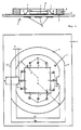
- the carrier element 1 has a flexible carrier substrate in the form of a flexible carrier film 2, on which conductor tracks, not shown on one or both sides, are provided.
- the carrier substrate 2 can consist of polyimide, fiber-reinforced epoxy (EPG) or polyester.
- the conductor tracks produce electrical connections between contact areas 4 and connection points 6.
- the electrical contact to an integrated circuit or semiconductor chip 7 is made via the connection points 6 by means of bonded gold wires 3.
- the contact to the semiconductor chip 7 is later made via the contact areas 4 when the finished chip card is used. 1, the contact surfaces 4 are on one side of the flexible carrier film 2 and the connection points 6 on the other side of the flexible carrier film.
- the semiconductor chip or crystal 7 is also arranged on the carrier film 2 on the side with the connection points 6.
- a stiffening ring 8 surrounding the semiconductor chip or semiconductor crystal 7 is also fastened on this side of the flexible carrier film.
- the stiffening ring 8 covers only a part of the surface of the carrier substrate 2.
- the stiffening ring 8 consists of the metal alloy CuSn6 with a hardness of 195 HV. The main mechanical properties of this material are shown in the table below.
- CuSn6 hard resilient double spring hard Tensile strength R m in N / mm 2 480-580 550-650 min. 630 0.2% proof stress R p 0.2 in N / mm 2 min. 450 min. 510 min. 600 Elongation at break A 5 % min. 20th 10th 6 A 10 % min. 15 8th - Vickers hardness 160-190 180-210 min. 200 Brinell hardness 150-180 170-200 min. 190 Spring bending limit R FB in N / mm 2 at least 350 160-190 in N / mm 2 at least 370 180-210
- the stiffening ring 8 and the semiconductor crystal 7 are by means of an adhesive layer 10 on the flexible carrier film 2 attached.
- the inside of the stiffening ring (8) is with a masking compound 11 filled so that the semiconductor crystals 7 together with bonding wires 3 from the covering compound 11 are surrounded.
- Fig. 2 shows the carrier element, 1 of Fig. 1 from above.
- the Stiffening ring 8 has a thickness of approximately 0.4 mm and can therefore easily be used in chip cards with a standard thickness of 0.76 mm (ISO standard) can be integrated.
- the stiffening ring 8 has on the outside there are two opposite straight areas 12 and 13.
- the straight areas 12 and 13 allow or facilitate the orientation of the stiffening ring 8 on the carrier film 2, since they are brands or markings for optical detection systems of handling machines serve.
- the outer diameter Da of the stiffening ring 8 measured at these straight areas 12 and 13 is approx.
- the inner diameter Di of the stiffening ring is 8.4 mm at these points.
- the projections 14 and 15 serve primarily for orientation of fully automatic bond machines.
- projections 14 and 15 also increase stability the narrower stiffening ring in the straight areas 12 and 13 8.
- the outer dimension is there through the ISO standard given.
- the depth T of these projections is approximately 0.5 mm and their width B about 1.4 mm.
- the shape of the Stiffening ring 8 according to FIG. 2 has a sufficient one high bending stiffness on the other hand this is Shape optimized for use in chip cards in accordance with the ISO standard.
- Semiconductor chips can be placed in the stiffening ring 8 according to FIG. 2 use up to a base area of up to 5.7 x 5.7 mm.
- the provision of brands for optical recognition systems allows a rational production of the support element with large
- the carrier element 1 according to the invention is preferred made in tape form, d. H. a plurality of successive carrier elements is in the form of a Ribbon provided.
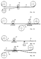
- Fig. 3 is used for explanation a first variant of a manufacturing process for the Support elements according to Fig. 1.
- the material for the stiffening ring 8th is in the form of a first volume 16.
- a double sided Adhesive tape 18 for forming the adhesive layer 10 will be provided.
- One side of the adhesive tape 18 is with covered with a protective film, not shown. Both tapes are in roll form.
- the two bands 16 and 18 are unrolled and fed to a pressing device 20. The The two tapes are brought together in such a way that the Side of the adhesive tape 18, which has no protective film glued to the first band 16 by the pressing device 20 becomes.
- the resulting combination tape 22 with the adhesive layer 10 can either be fed directly to a ring punch 24 or rolled up again and at a later date to be processed further.
- the ring punch 24 punches out of the Combination band 22 the stiffening ring 8 in the desired shape out.
- the ring punch 24 is, however, designed so that the Stiffening ring 8 remains in the combination band 22, so that processed the combination belt 22 with the stiffening ring 8 can be.
- the next step is the flexible in the form of a second band 26 Carrier film 2 merged with the combination tape 22 and the two bands 22 and 26 are relative to each other in one Positioning and pressing device 28 positioned so that the Stiffening ring 8 in the desired position over the connection points 6 comes to rest.
- the stiffening ring 8 from the combination band 22 pushed out and in the desired position with the second tape 26 glued This must be done beforehand, preferably between Ring punch 24 and feeding the second tape 26, the protective film still on the combination belt 22 is removed (not shown).
- the remaining combination tape 22 without stiffening ring 8 can be collected and the resulting support elements 1 with stiffening ring 8 in Form of an endless belt can either also be rolled up be or immediately the further processing, the equipping with the semiconductor crystal 7, are supplied.
- Fig. 4 shows a second variant of a method for manufacturing of the carrier elements according to Fig. 1.
- Fig. 4 are corresponding Provide components with the same reference numerals as in Fig. 3.
- the schematically shown in Fig. 4 The method differs from the method according to FIG. 3 only in that the adhesive layer 10 is not in shape a double-sided adhesive tape applied to the first tape is, but directly using an adhesive spray device 30 is applied to the first band 16. Since the adhesive layer 10 is then present without a protective film the adhesive layer 10 only after punching out the stiffening ring 8 performed in the ring punch 24.
- the one with the Combination tape 22 provided with adhesive layer 10 is then immediately the pressing and positioning device 28, the likewise the flexible carrier film 2 in the form of the second Band 26 is fed.
- the further process steps correspond to the method according to FIG. 3.
- Carrier elements 1 in the form of a ribbon are then also fully automatic with one or more semiconductor crystals 7 and the interior of the stiffening ring 8 with the semiconductor crystal 7 and connecting wires 3 then poured out with the covering compound 11. If the masking compound 11 is cured, if necessary, excess Masking compound sanded. Equipping the carrier film or carrier substrates 2 with the semiconductor crystals 7 by means of known methods or with known fully automatic Pick and place machines and bond machines. Pouring the inside of the stiffening ring 8 with the casting or covering compound 11 is done in a known manner. The resulting one or more semiconductor circuits equipped carrier elements 1 can then be separated and built into chip cards, for example. In The separation of the individually finished components is advantageously carried out Support elements only immediately before or at Installation in the chip cards.
- the support element described above is Particularly suitable for installation in chip cards according to the ISO standard and designed.
- the carrier elements according to the invention can of course also be used in other circuits and devices install, exposed to mechanical stress are.
- FIG. 5 shows a sectional view of a first embodiment an inventive chip card 36.
- the chip card 36 has a card body 37 with an integrated therein Carrier element 1 on which the integrated circuit 7 is glued on.
- the carrier element 1 with the semiconductor chip 7 is in a corresponding recess 38 of the card body 37 embedded.
- the top of the stiffening ring 8 will by a cover layer 40, which is part of the card body 37 is covered.
- the underside of the carrier element 1 and the Carrier film 2 is aligned with one side of chip card 36, see above that the contact surfaces 4 from this side of the chip card 36 are accessible.
- the chip card 50 also has a card body 52 into which the carrier element according to the invention 1 is integrated with IC.
- the card body 52 is made from four laminate layers, an upper cover layer 54, a middle layer 55, a leveling layer 56 and a lower cover layer 57 which is used in the manufacture of the Chip card 50 pressed under hot pressure to card body 52 become.
- the middle layer 55. the compensation layer 56 and the lower cover layer 57 have recesses which are together form a recess 58, which the carrier element 1 fills out.
- the top cover layer 54 covers the reinforcement ring 8.
- the middle layer then follows as the next laminate layer 55, whose thickness is less than the height of the reinforcement ring 8 and has a recess that the Cross section of the reinforcement ring 8 corresponds.
- the compensation layer 56 the thickness of which is equal to the thickness of the Carrier substrate 2 is.
- the compensation layer 56 has one Recess on which corresponds to the surface of the carrier element 1 and which is therefore larger than the recess in the Middle layer 55.
- the lower cover layer 57 the other side of the carrier element 1 and so that the carrier substrate 2 covers and only the contact surfaces 4 leaves freely accessible. It doesn't just make the whole thing Carrier element 1 sandwiched by laminate layers, but also not from the reinforcement ring 8 covered part of the flexible carrier substrate 2.
- the support element 1 is held in the card body 52 additionally improved by the fact that the Reinforcement ring 8 covers part of the carrier substrate 2 is arranged deeper in the finished card body 52 than the part of the carrier substrate covered by the reinforcing ring 8 2.
- This forms the of the stiffening ring 8th covered part of the carrier substrate 2 in a flat trough not covered by the stiffening ring 8 part of the carrier substrate 2.
- a particularly flexible carrier substrate 2 must be used.
- a film made of polyimide is particularly suitable for this because of their temperature stability up to 250 ° C and their high Flexibility.
- the thickness of the foils used is approx. 100 ⁇ m.
- Access to the semiconductor crystal embedded in the chip card can instead of over contact areas also done via induction loops. This has the advantage that upper and lower cover layers none Must have recesses, d. H. is the carrier element completely embedded in the card body.
- Carrier element with several arranged side by side Install stiffening rings in a chip card.
Landscapes
- Engineering & Computer Science (AREA)
- Computer Hardware Design (AREA)
- Microelectronics & Electronic Packaging (AREA)
- Physics & Mathematics (AREA)
- General Physics & Mathematics (AREA)
- Theoretical Computer Science (AREA)
- Credit Cards Or The Like (AREA)
- Structures Or Materials For Encapsulating Or Coating Semiconductor Devices Or Solid State Devices (AREA)
Abstract
Description
- Fig. 1
- Eine Schnittansicht einer bevorzugten Ausführungsform des Trägerelements mit IC;
- Fig. 2
- eine Aufsicht auf die Ausführungsform nach Fig. 1;
- Fig. 3
- eine schematische Darstellung einer ersten Variante eines Herstellungsverfahrens für die Trägerelemente nach Fig. 1;
- Fig. 4
- eine zweite Variante eines Herstellungsverfahrens für die Trägerelemente nach Fig. 1;
- Fig. 5
- einen Schnitt durch eine erste Ausführungsform einer Chip-Karte mit dem Trägerelement nach Fig. 1; und
- Fig. 6
- einen Schnitt durch eine weitere Ausführungsform einer Chip-Karte mit dem erfindungsgemäßen Trägerelement.
| CuSn6 | hart | federhart | doppelfederhart |
| Zugfestigkeit Rm in N/mm2 | 480-580 | 550-650 | min. 630 |
| 0,2 %-Dehngrenze Rp 0,2 in N/mm2 | min. 450 | min. 510 | min. 600 |
| Bruchdehnung | |||
| A5 % min. | 20 | 10 | 6 |
| A10 % min. | 15 | 8 | - |
| Vickershärte | 160-190 | 180-210 | min. 200 |
| Brinellhärte | 150-180 | 170-200 | min. 190 |
| Federbiegegrenze RFB | |||
| in N/mm2 mind.350 | 160-190 | ||
| in N/mm2 mind.370 | 180-210 |
Claims (18)
- Trägerelement mit mit wenigstens einem integrierten Schaltkreis (7) in Form eines Halbleiterkristalls insbesondere für den Einbau in Chip-Karten, miteinem flexiblen Trägersubstrat (2), auf dessen Oberfläche mehrere Kontaktflächen (4) vorgesehen sind, die über Leiterbahnen mit Anschlußpunkten (6) für den wenigstens einen integrierten Schaltkreis (7) verbunden sind, undeinem Versteifungsring (8), der auf dem flexiblen Trägersubstrat befestigt ist, der eine innere Teilfläche des Trägersubstrats (2) umschließt und der auch außen von einer periphären Teilfläche des Trägersubstrats(2) umgeben ist, wobei der bzw. die integrierten Schaltkreise (7) auf der inneren Teilfläche angeordnet ist bzw. sind, dadurch gekennzeichnet,daß zumindest die von dem Verstärkungsring (8) bedeckten und umschlossenen Bereiche des flexiblen Trägersubstrats (2) durchgehend ebene Flächen bilden,daß der Versteifungsring (8) eine wesentlich höhere Biegesteifigkeit aufweist, als das flexible Trägersubstrat (2), so daß sich bei Verbiegung des flexiblen Trägersubstrats (2) der Versteifungsring (8) nicht verbiegt,daß die Dicke des Versteifungsrings (8) kleiner ist als seine Breite, unddaß der Versteifungsring (8) im Verbund mit dem flexiblen Trägersubstrat (2) als verwindungssteife Zelle wirkt und dadurch den Halbleiterkristall (7) vor mechanischen Beanspruchungen schützt.
- Trägerelement nach Anspruch 1, dadurch gekennzeichnet, daß die Breite des Versteifungsrings (8) in Richtung des Durchmessers ca. 1,5 mm und die Dicke des Versteifungsrings ca. 0,4 mm beträgt.
- Trägerelement nach Anspruch 1 oder 2, dadurch gekennzeichnet, daß der Versteifungsring (8) kreisringförmig ist.
- Trägerelement nach einem der vorhergehenden Ansprüche, dadurch gekennzeichnet, daß das Material, aus dem der Versteifungsring (8) besteht einen Elastizitätsmodul aufweist, das größer als 500 N/mm2 ist.
- Trägerelement nach einem der vorhergehenden Ansprüche, dadurch gekennzeichnet, daß der Versteifungsring (8) aus Metall bzw. einer Metall-Legierung besteht.
- Trägerelement nach Anspruch 5, dadurch gekennzeichnet, daß der Versteifungsring (8) aus CuSn6, 195 HV oder CrNi 17/7, 220 HV besteht.
- Trägerelement nach einem der vorhergehenden Ansprüche, dadurch gekennzeichnet, daß der Versteifungsring (8) mit dem flexiblen Trägersubstrat (2) verklebt ist.
- Trägerelement nach einem der vorhergehenden Ansprüche, dadurch gekennzeichnet, daß der Versteifungsring (8) Marken (12, 14) für optische Erkennungssysteme aufweist.
- Trägerelement nach Anspruch 8, dadurch gekennzeichnet, daß die Marken (12, 14) zapfenförmige Vorsprünge (14) umfassen, die in das Innere des Versteifungsrings (8) weisen.
- Trägerelement nach Anspruch 8 oder 9, dadurch gekennzeichnet, daß die Marken (12, 14) gerade Bereiche (12) am äußeren Rand des Versteifungsringes (8) umfassen.
- Trägerelement nach einem der vorhergehenden Ansprüche, dadurch gekennzeichnet, daß das flexible Trägersubstrat (2) aus Polyimid besteht.
- Chip-Karte mit wenigstens einem integrierten Schaltkreis, der auf einem Trägerelement angeordnet ist, gekennzeichnet durch ein Trägerelement (1) nach einem der Ansprüche 1 bis 11.
- Chip-Karte nach Anspruch 12, dadurch gekennzeichnet, daß es sich um eine Chip-Karte in ISO-Norm handelt.
- Chip-Karte nach einem der Ansprüche 12 bis 13, dadurch gekennzeichnet, daß der Teil des Trägersubstrats (2), der von dem Versteifungsring (8) umfaßt und überdeckt ist, eine flache Mulde in dem übrigen Teil des Trägersubstrats (2) bildet, der nicht von dem Versteifungsring (8) umfaßt und überdeckt wird, so daß der übrige Teil des Trägersubstrats (2) tiefer im Chip-Kartenkörper angeordnet ist.
- Verfahren zur Herstellung eines Trägerelements nach einem der Ansprüche 1 bis 11 mit den Verfahrensschritten:a) Bereitstellen des Materials für den Versteifungsring (8) in Form eines ersten Bandes (16);b) Bereitstellen des flexiblen Trägersubstrats (2) mit Leiterbahnen, Kontaktflächen (4) und Anschlußpunkten (6) für integrierte Schaltkreise in Form eines zweiten Bandes (26);c) Versehen des ersten Bandes (16) mit einer Klebeschicht (10), so daß ein Kombi-Band (22) entsteht;d) Ausstanzen des Versteifungsringes (8) aus dem Kombi-Band (22) derart, daß die Dicke des Versteifungsrings kleiner ist als seine Breite in Richtung des Durchmessers und der Versteifungsring (8) in dem Kombi-Band (22) verbleibt;e) Zusammenführen des Kombi-Bandes (22) mit dem ausgestanzten Versteifungsring (8) und dem zweiten Band (26) und Positionieren der Versteifungsringe (8) in dem Kombi-Band (22) über den Anschlußpunkten (6) für integrierte Schaltkreise auf dem zweiten Band (26);f) Trennen der Versteifungsringe (8) von dem Kombi-Band (22) und Verkleben der positionierten Versteifungsringe (8) mit dem zweiten Band (26).g) Bestücken des zweiten Bandes (26) mit wenigstens einem integrierten Schaltkreis (7) und Herstellen der elektrischen Verbindungen zwischen den Anschlußpunkten (6) und dem integrierten Schaltkreis; undh) Ausfüllen des Inneren des Versteifungsrings (8) mit einer Abdeckmasse (11).
- Verfahren nach Anspruch 15, dadurch gekennzeichnet, daß die Verfahrensschritte c) und d) vertauscht sind.
- Verfahren nach Anspruch 15 oder 16, dadurch gekennzeichnet, daß im Vefahrensschritt c) ein doppelseitiges Klebeband (18) mit dem ersten Band (16) verpreßt wird.
- Verfahren nach Anspruch 15 oder 16, dadurch gekennzeichnet, daß im Verfahrensschritt c) die Klebeschicht (10) auf das erste Band aufgesprüht wird.
Priority Applications (1)
| Application Number | Priority Date | Filing Date | Title |
|---|---|---|---|
| AT90910564T ATE99439T1 (de) | 1989-07-24 | 1990-07-23 | Traegerelement mit wenigstens einem integrierten schaltkreis, insbesondere zum einbau in chipkarten. |
Applications Claiming Priority (3)
| Application Number | Priority Date | Filing Date | Title |
|---|---|---|---|
| DE3924439A DE3924439A1 (de) | 1989-07-24 | 1989-07-24 | Traegerelement mit wenigstens einem integrierten schaltkreis, insbesondere zum einbau in chip-karten, sowie verfahren zur herstellung dieser traegerelemente |
| DE3924439 | 1989-07-24 | ||
| PCT/DE1990/000559 WO1991001533A1 (de) | 1989-07-24 | 1990-07-23 | Trägerelement mit wenigstens einem integrierten schaltkreis, insbesondere zum einbau in chip-karten |
Publications (3)
| Publication Number | Publication Date |
|---|---|
| EP0484353A1 EP0484353A1 (de) | 1992-05-13 |
| EP0484353B1 EP0484353B1 (de) | 1993-12-29 |
| EP0484353B2 true EP0484353B2 (de) | 2000-11-29 |
Family
ID=6385706
Family Applications (1)
| Application Number | Title | Priority Date | Filing Date |
|---|---|---|---|
| EP90910564A Expired - Lifetime EP0484353B2 (de) | 1989-07-24 | 1990-07-23 | Trägerelement mit wenigstens einem integrierten schaltkreis, insbesondere zum einbau in chip-karten |
Country Status (5)
| Country | Link |
|---|---|
| EP (1) | EP0484353B2 (de) |
| DD (1) | DD298170A5 (de) |
| DE (2) | DE3924439A1 (de) |
| ES (1) | ES2064741T5 (de) |
| WO (1) | WO1991001533A1 (de) |
Cited By (1)
| Publication number | Priority date | Publication date | Assignee | Title |
|---|---|---|---|---|
| DE102008054932A1 (de) * | 2008-12-18 | 2010-07-01 | Infineon Technologies Ag | Leistungshalbleitermodul mit versteifter Bodenplatte |
Families Citing this family (44)
| Publication number | Priority date | Publication date | Assignee | Title |
|---|---|---|---|---|
| CA2051836C (en) * | 1990-11-30 | 1996-07-23 | Richard Michael Flynn | Personal data card construction |
| DE9100665U1 (de) * | 1991-01-21 | 1992-07-16 | TELBUS Gesellschaft für elektronische Kommunikations-Systeme mbH, 85391 Allershausen | Trägerelement für integrierte Halbleiter-Schaltkreise, insbesondere zum Einbau in Chip-Karten |
| FR2673039A1 (fr) * | 1991-02-18 | 1992-08-21 | Em Microelectronic Marin Sa | Module protege pour carte a microcircuits. |
| DE4105869C2 (de) * | 1991-02-25 | 2000-05-18 | Edgar Schneider | IC-Karte und Verfahren zu ihrer Herstellung |
| DE9113601U1 (de) * | 1991-10-31 | 1993-03-04 | Schneider, Edgar, 8057 Günzenhausen | Multifunktionaler Schutzschild für mikroelektronische Schaltungen und Sensoren insbesondere für sog. Chip-Karten |
| DE9114033U1 (de) * | 1991-11-12 | 1993-03-18 | Teltron GmbH, 99842 Ruhla | Programmierbares elektronisches Potentiometer |
| DE4224103A1 (de) * | 1992-07-22 | 1994-01-27 | Manfred Dr Ing Michalk | Miniaturgehäuse mit elektronischen Bauelementen |
| CH686325A5 (de) * | 1992-11-27 | 1996-02-29 | Esec Sempac Sa | Elektronikmodul und Chip-Karte. |
| DE4336501A1 (de) * | 1993-10-26 | 1995-04-27 | Giesecke & Devrient Gmbh | Verfahren zur Herstellung von Ausweiskarten mit elektronischen Modulen |
| DE4340847A1 (de) * | 1993-11-26 | 1995-06-01 | Optosys Gmbh Berlin | Chipmodul und Verfahren zur Herstellung eines Chipmoduls |
| JPH07214957A (ja) * | 1994-01-31 | 1995-08-15 | Mitsubishi Electric Corp | Icカード |
| DE4403753C1 (de) * | 1994-02-08 | 1995-07-20 | Angewandte Digital Elektronik | Kombinierte Chipkarte |
| EP0692771A3 (de) * | 1994-07-15 | 1997-07-16 | Shinko Name Plate Kabushiki Ka | Speicherkarte und Verfahren zur Herstellung |
| KR100355209B1 (ko) * | 1994-09-22 | 2003-02-11 | 로무 가부시키가이샤 | 비접촉형ic카드및그제조방법 |
| DE19509233A1 (de) * | 1995-03-19 | 1996-09-26 | Melzer Maschinenbau Gmbh | Verfahren zum Herstellen von Elektronik-Komponenten enthaltenden Kunststoffkarten |
| CA2192076C (en) * | 1995-04-13 | 2000-01-18 | Masao Gogami | Ic card and ic module |
| FR2735257B1 (fr) * | 1995-06-09 | 1997-08-29 | Solaic Sa | Carte laminee a circuit integre |
| DE19602436B4 (de) * | 1996-01-24 | 2006-09-14 | Infineon Technologies Ag | Verfahren zur Montage eines Rahmens auf ein Trägermaterial und Vorrichtung zur Durchführung des Verfahrens |
| DE19607212C1 (de) * | 1996-02-26 | 1997-04-10 | Richard Herbst | Verbundkörper, Verfahren und Kunststoff-Spritzgießwerkzeug zur Herstellung eines solchen |
| DE19637215C2 (de) * | 1996-08-22 | 2001-03-01 | Pav Card Gmbh | Verbindungsanordnung zur Herstellung einer Chipkarte |
| DE19610507C2 (de) * | 1996-03-15 | 1997-12-04 | David Finn | Chipkarte |
| DE19654902C2 (de) * | 1996-03-15 | 2000-02-03 | David Finn | Chipkarte |
| ATE212752T1 (de) * | 1996-06-14 | 2002-02-15 | Infineon Technologies Ag | Verfahren zur herstellung eines trägerelements für halbleiterchips |
| DE19623826C2 (de) * | 1996-06-14 | 2000-06-15 | Siemens Ag | Verfahren zur Herstellung eines Trägerelements für Halbleiterchips |
| DE19632117C1 (de) * | 1996-08-08 | 1997-12-18 | Siemens Ag | Datenträger zur kontaktlosen Übertragung von elektrischen Signalen |
| DE19632813C2 (de) * | 1996-08-14 | 2000-11-02 | Siemens Ag | Verfahren zur Herstellung eines Chipkarten-Moduls, unter Verwendung dieses Verfahrens hergestellter Chipkarten-Modul und diesen Chipkarten-Modul enthaltende Kombi-Chipkarte |
| DE19640304C2 (de) | 1996-09-30 | 2000-10-12 | Siemens Ag | Chipmodul insbesondere zur Implantation in einen Chipkartenkörper |
| US6088901A (en) * | 1997-06-10 | 2000-07-18 | Siemens Aktiengesellschaft | Method for producing a carrier element for semiconductor chips |
| SE518572C2 (sv) * | 1997-08-25 | 2002-10-22 | Ericsson Telefon Ab L M | Bärarelement för ett chips samt chipsmodul |
| FR2769110B1 (fr) * | 1997-09-26 | 1999-12-03 | Gemplus Card Int | Procede de fabrication d'un module ou etiquette electronique, module ou etiquette obtenue et support comportant un tel module ou etiquette |
| DE19803020C2 (de) | 1998-01-27 | 1999-12-02 | Siemens Ag | Chipkartenmodul für biometrische Sensoren |
| FR2790850B1 (fr) * | 1999-03-12 | 2004-02-27 | Gemplus Card Int | Procede de fabrication de dispositif electronique portable de type carte a puce |
| FR2799857A1 (fr) * | 1999-10-14 | 2001-04-20 | Gemplus Card Int | Procede pour le renforcement d'un module de circuit integre de carte a puce |
| EP1174821A1 (de) * | 2000-07-20 | 2002-01-23 | Sokymat S.A. | Transponder mit Versteifungselement |
| DE10111028A1 (de) * | 2001-03-07 | 2002-09-19 | Infineon Technologies Ag | Chipkartenmodul |
| DE10143108A1 (de) * | 2001-09-03 | 2003-04-03 | Infineon Technologies Ag | Chipkartenmodul mit einem eine integrierte Schaltung aufweisenden Chip |
| DE10200382B4 (de) * | 2002-01-08 | 2006-05-04 | Infineon Technologies Ag | Chipmodul für Chipkarten |
| DE102004056829A1 (de) * | 2004-11-24 | 2006-06-01 | Bundesdruckerei Gmbh | Trägermaterial sowie Verfahren zur Herstellung eines Wertdokumentes |
| EP2131392A4 (de) * | 2007-03-23 | 2011-08-24 | Fujitsu Ltd | Elektronische anordnung, eine elektronische anordnung anbringende elektronische vorrichtung, einen artikel anbringende elektronische anordnung und verfahren zur herstellung einer elektronischen anordnung |
| CN101636837B (zh) * | 2007-03-23 | 2011-07-27 | 富士通株式会社 | 电子装置、安装有电子装置的电子设备、安装有电子装置的物品、电子装置的制造方法 |
| CN101636750B (zh) * | 2007-03-23 | 2012-08-08 | 富士通株式会社 | 电子装置、安装有电子装置的电子设备、安装有电子装置的物品、电子装置的制造方法 |
| US7851334B2 (en) * | 2007-07-20 | 2010-12-14 | Infineon Technologies Ag | Apparatus and method for producing semiconductor modules |
| GB2584106B (en) | 2019-05-21 | 2024-03-27 | Pragmatic Printing Ltd | Flexible electronic structure |
| EP4511880B1 (de) * | 2022-05-09 | 2025-08-27 | Linxens Holding | Vorverpackung für eine leiterplatte für eine chipkarte und herstellungsverfahren dafür |
Citations (2)
| Publication number | Priority date | Publication date | Assignee | Title |
|---|---|---|---|---|
| JPS61145696A (ja) † | 1984-12-19 | 1986-07-03 | Matsushita Electric Ind Co Ltd | Icカ−ド |
| EP0201952A1 (de) † | 1985-04-12 | 1986-11-20 | Philips Composants | Verfahren und Einrichtung zur Herstellung einer elektronischen Identifikationskarte |
Family Cites Families (14)
| Publication number | Priority date | Publication date | Assignee | Title |
|---|---|---|---|---|
| FR2337381A1 (fr) * | 1975-12-31 | 1977-07-29 | Honeywell Bull Soc Ind | Carte portative pour systeme de traitement de signaux electriques et procede de fabrication de cette carte |
| FR2439478A1 (fr) * | 1978-10-19 | 1980-05-16 | Cii Honeywell Bull | Boitier plat pour dispositifs a circuits integres |
| DE2920012C2 (de) * | 1979-05-17 | 1988-09-29 | GAO Gesellschaft für Automation und Organisation mbH, 8000 München | Ausweiskarte mit IC-Baustein und Verfahren zur Herstellung einer derartigen Ausweiskarte |
| DE3029667A1 (de) * | 1980-08-05 | 1982-03-11 | GAO Gesellschaft für Automation und Organisation mbH, 8000 München | Traegerelement fuer einen ic-baustein |
| DE3235650A1 (de) * | 1982-09-27 | 1984-03-29 | Philips Patentverwaltung Gmbh, 2000 Hamburg | Informationskarte und verfahren zu ihrer herstellung |
| DE3248385A1 (de) * | 1982-12-28 | 1984-06-28 | GAO Gesellschaft für Automation und Organisation mbH, 8000 München | Ausweiskarte mit integriertem schaltkreis |
| US4727246A (en) * | 1984-08-31 | 1988-02-23 | Casio Computer Co., Ltd. | IC card |
| FR2579798B1 (fr) * | 1985-04-02 | 1990-09-28 | Ebauchesfabrik Eta Ag | Procede de fabrication de modules electroniques pour cartes a microcircuits et modules obtenus selon ce procede |
| FR2588695B1 (fr) * | 1985-10-11 | 1988-07-29 | Eurotechnique Sa | Procede de fabrication d'un microboitier, microboitier a contacts effleurants et application aux cartes contenant des composants |
| DE3602596A1 (de) * | 1986-01-29 | 1987-07-30 | Telefunken Electronic Gmbh | Zentriervorrichtung zur automatischen bearbeitung von komponenten elektronischer bauelemente |
| JP2502511B2 (ja) * | 1986-02-06 | 1996-05-29 | 日立マクセル株式会社 | 半導体装置の製造方法 |
| JPH0517268Y2 (de) * | 1986-04-16 | 1993-05-10 | ||
| FR2599893B1 (fr) * | 1986-05-23 | 1996-08-02 | Ricoh Kk | Procede de montage d'un module electronique sur un substrat et carte a circuit integre |
| DE3623419A1 (de) * | 1986-07-11 | 1988-01-21 | Junghans Uhren Gmbh | Verfahren zum bestuecken eines leiterbahnen-netzwerkes fuer den schaltungstraeger eines elektromechanischen uhrwerks und teilbestuecktes leiterbahnen-netzwerk eines uhrwerks-schaltungstraegers |
-
1989
- 1989-07-24 DE DE3924439A patent/DE3924439A1/de not_active Ceased
-
1990
- 1990-07-23 WO PCT/DE1990/000559 patent/WO1991001533A1/de not_active Ceased
- 1990-07-23 ES ES90910564T patent/ES2064741T5/es not_active Expired - Lifetime
- 1990-07-23 EP EP90910564A patent/EP0484353B2/de not_active Expired - Lifetime
- 1990-07-23 DE DE90910564T patent/DE59004053D1/de not_active Expired - Fee Related
- 1990-07-24 DD DD90343044A patent/DD298170A5/de not_active IP Right Cessation
Patent Citations (2)
| Publication number | Priority date | Publication date | Assignee | Title |
|---|---|---|---|---|
| JPS61145696A (ja) † | 1984-12-19 | 1986-07-03 | Matsushita Electric Ind Co Ltd | Icカ−ド |
| EP0201952A1 (de) † | 1985-04-12 | 1986-11-20 | Philips Composants | Verfahren und Einrichtung zur Herstellung einer elektronischen Identifikationskarte |
Non-Patent Citations (1)
| Title |
|---|
| "Einführung in die DIN-Normen", 8. Auflage, Teubner Verlag, S. 444, Tabelle 444.1 † |
Cited By (2)
| Publication number | Priority date | Publication date | Assignee | Title |
|---|---|---|---|---|
| DE102008054932A1 (de) * | 2008-12-18 | 2010-07-01 | Infineon Technologies Ag | Leistungshalbleitermodul mit versteifter Bodenplatte |
| DE102008054932B4 (de) * | 2008-12-18 | 2011-12-01 | Infineon Technologies Ag | Leistungshalbleitermodul mit versteifter Bodenplatte |
Also Published As
| Publication number | Publication date |
|---|---|
| DE59004053D1 (de) | 1994-02-10 |
| DE3924439A1 (de) | 1991-04-18 |
| ES2064741T3 (es) | 1995-02-01 |
| EP0484353A1 (de) | 1992-05-13 |
| ES2064741T5 (es) | 2001-02-16 |
| EP0484353B1 (de) | 1993-12-29 |
| WO1991001533A1 (de) | 1991-02-07 |
| DD298170A5 (de) | 1992-02-06 |
Similar Documents
| Publication | Publication Date | Title |
|---|---|---|
| EP0484353B2 (de) | Trägerelement mit wenigstens einem integrierten schaltkreis, insbesondere zum einbau in chip-karten | |
| EP0299530B1 (de) | Trägerelement zum Einbau in Ausweiskarten | |
| DE102005058101B4 (de) | Chipkarte und Verfahren zur Herstellung einer Chipkarte | |
| DE69806515T2 (de) | Elektronische vorrichtung mit wegwerfchip und verfahren zu deren herstellung | |
| DE68921179T2 (de) | Elektronisches Modul mit einer integrierten Schaltung für ein kleines tragbares Objekt, z.B. eine Karte oder ein Schlüssel und Herstellungsverfahren für solche Module. | |
| DE3153768C2 (de) | Ausweiskarte | |
| DE69512137T2 (de) | Herstellungsverfahren und Montage für IC-Karte. | |
| EP0554916A2 (de) | Baustein mit integrierten Schaltkreisen | |
| DE2333813C3 (de) | Ebene Magnetkopfanordnung mit mehreren flachen Magnetkopfstrukturen | |
| EP0723244A2 (de) | Datenträger mit einem elektronischen Modul | |
| CH686325A5 (de) | Elektronikmodul und Chip-Karte. | |
| DE4040770C2 (de) | Datenträger mit integriertem Schaltkreis | |
| DE4122049A1 (de) | Verfahren zum einbau eines traegerelements | |
| DE19610507C2 (de) | Chipkarte | |
| DE19623826C2 (de) | Verfahren zur Herstellung eines Trägerelements für Halbleiterchips | |
| EP0568572B1 (de) | Trägerelement für integrierte halbleiter-schaltkreise, insbesondere zum einbau in chip-karten | |
| EP0591668A1 (de) | Verfahren zur Montage von integrierten Halbleiterschaltkreisen | |
| DE602004004647T2 (de) | Verfahren zum zusammenbauen eines elektronischen komponent auf einem substrat | |
| DE19633654A1 (de) | Elektronische Mikrogehäuse für eine elektronische Speicherkarte und Verfahren zur Herstellung derselben | |
| DE10324043B4 (de) | Kartenförmiger elektronischer Datenträger, Funktionsinlett dafür und ihre Herstellungsverfahren | |
| DE102014108916B4 (de) | Bandförmiges Substrat zur Herstellung von Chipträgern, elektronisches Modul mit einem solchen Chipträger, elektronische Einrichtung mit einem solchen Modul und Verfahren zur Herstellung eines Substrates | |
| EP1185954B1 (de) | Chip-träger-verbund | |
| EP1925192B1 (de) | Laminiertes substrat für die montage von elektronischen bauteilen | |
| DE19929912A1 (de) | Trägerelement für einen IC-Baustein | |
| WO1997042655A1 (de) | Trägerelement mit wenigstens einem integrierten schaltkreis sowie verfahren zur herstellung eines solchen trägerelementes |
Legal Events
| Date | Code | Title | Description |
|---|---|---|---|
| PUAI | Public reference made under article 153(3) epc to a published international application that has entered the european phase |
Free format text: ORIGINAL CODE: 0009012 |
|
| 17P | Request for examination filed |
Effective date: 19920224 |
|
| AK | Designated contracting states |
Kind code of ref document: A1 Designated state(s): AT BE CH DE ES FR GB IT LI NL |
|
| 17Q | First examination report despatched |
Effective date: 19920811 |
|
| GRAA | (expected) grant |
Free format text: ORIGINAL CODE: 0009210 |
|
| AK | Designated contracting states |
Kind code of ref document: B1 Designated state(s): AT BE CH DE ES FR GB IT LI NL |
|
| REF | Corresponds to: |
Ref document number: 99439 Country of ref document: AT Date of ref document: 19940115 Kind code of ref document: T |
|
| ITF | It: translation for a ep patent filed | ||
| GBT | Gb: translation of ep patent filed (gb section 77(6)(a)/1977) |
Effective date: 19940111 |
|
| REF | Corresponds to: |
Ref document number: 59004053 Country of ref document: DE Date of ref document: 19940210 |
|
| ET | Fr: translation filed | ||
| PLBI | Opposition filed |
Free format text: ORIGINAL CODE: 0009260 |
|
| 26 | Opposition filed |
Opponent name: GIESECKE & DEVRIENT GMBH Effective date: 19940928 |
|
| NLR1 | Nl: opposition has been filed with the epo |
Opponent name: GIESECKE & DEVRIENT GMBH |
|
| REG | Reference to a national code |
Ref country code: ES Ref legal event code: FG2A Ref document number: 2064741 Country of ref document: ES Kind code of ref document: T3 |
|
| PLAB | Opposition data, opponent's data or that of the opponent's representative modified |
Free format text: ORIGINAL CODE: 0009299OPPO |
|
| PGFP | Annual fee paid to national office [announced via postgrant information from national office to epo] |
Ref country code: CH Payment date: 19950807 Year of fee payment: 6 |
|
| R26 | Opposition filed (corrected) |
Opponent name: GIESECKE & DEVRIENT GMBH Effective date: 19940928 |
|
| NLR1 | Nl: opposition has been filed with the epo |
Opponent name: GIESECKE & DEVRIENT GMBH |
|
| PG25 | Lapsed in a contracting state [announced via postgrant information from national office to epo] |
Ref country code: LI Effective date: 19960731 Ref country code: CH Effective date: 19960731 |
|
| PLBL | Opposition procedure terminated |
Free format text: ORIGINAL CODE: EPIDOS OPPC |
|
| PLBM | Termination of opposition procedure: date of legal effect published |
Free format text: ORIGINAL CODE: 0009276 |
|
| PLAW | Interlocutory decision in opposition |
Free format text: ORIGINAL CODE: EPIDOS IDOP |
|
| D27C | Opposition proceedings terminated (deleted) | ||
| REG | Reference to a national code |
Ref country code: CH Ref legal event code: PL |
|
| APAC | Appeal dossier modified |
Free format text: ORIGINAL CODE: EPIDOS NOAPO |
|
| NLR2 | Nl: decision of opposition | ||
| APAC | Appeal dossier modified |
Free format text: ORIGINAL CODE: EPIDOS NOAPO |
|
| APAC | Appeal dossier modified |
Free format text: ORIGINAL CODE: EPIDOS NOAPO |
|
| APAE | Appeal reference modified |
Free format text: ORIGINAL CODE: EPIDOS REFNO |
|
| APAC | Appeal dossier modified |
Free format text: ORIGINAL CODE: EPIDOS NOAPO |
|
| PLAW | Interlocutory decision in opposition |
Free format text: ORIGINAL CODE: EPIDOS IDOP |
|
| PLAW | Interlocutory decision in opposition |
Free format text: ORIGINAL CODE: EPIDOS IDOP |
|
| PGFP | Annual fee paid to national office [announced via postgrant information from national office to epo] |
Ref country code: ES Payment date: 20000731 Year of fee payment: 11 |
|
| PUAH | Patent maintained in amended form |
Free format text: ORIGINAL CODE: 0009272 |
|
| STAA | Information on the status of an ep patent application or granted ep patent |
Free format text: STATUS: PATENT MAINTAINED AS AMENDED |
|
| 27A | Patent maintained in amended form |
Effective date: 20001129 |
|
| AK | Designated contracting states |
Kind code of ref document: B2 Designated state(s): AT BE CH DE ES FR GB IT LI NL |
|
| ITF | It: translation for a ep patent filed | ||
| REG | Reference to a national code |
Ref country code: CH Ref legal event code: AEN Free format text: AUFRECHTERHALTUNG DES PATENTES IN GEAENDERTER FORM |
|
| GBTA | Gb: translation of amended ep patent filed (gb section 77(6)(b)/1977) | ||
| ET3 | Fr: translation filed ** decision concerning opposition | ||
| NLR2 | Nl: decision of opposition | ||
| NLR3 | Nl: receipt of modified translations in the netherlands language after an opposition procedure | ||
| NLXE | Nl: other communications concerning ep-patents (part 3 heading xe) |
Free format text: PAT. BUL. 05/97 PAGE 742: THE DECISION OF WITHDRAWALL OPPOSITION SHOULD BE DELETED. |
|
| REG | Reference to a national code |
Ref country code: ES Ref legal event code: DC2A Kind code of ref document: T5 Effective date: 20010104 |
|
| PGFP | Annual fee paid to national office [announced via postgrant information from national office to epo] |
Ref country code: NL Payment date: 20010731 Year of fee payment: 12 Ref country code: AT Payment date: 20010731 Year of fee payment: 12 |
|
| PGFP | Annual fee paid to national office [announced via postgrant information from national office to epo] |
Ref country code: GB Payment date: 20010808 Year of fee payment: 12 |
|
| PGFP | Annual fee paid to national office [announced via postgrant information from national office to epo] |
Ref country code: BE Payment date: 20010810 Year of fee payment: 12 |
|
| PGFP | Annual fee paid to national office [announced via postgrant information from national office to epo] |
Ref country code: FR Payment date: 20010821 Year of fee payment: 12 |
|
| REG | Reference to a national code |
Ref country code: GB Ref legal event code: IF02 |
|
| PG25 | Lapsed in a contracting state [announced via postgrant information from national office to epo] |
Ref country code: GB Free format text: LAPSE BECAUSE OF NON-PAYMENT OF DUE FEES Effective date: 20020723 Ref country code: AT Free format text: LAPSE BECAUSE OF NON-PAYMENT OF DUE FEES Effective date: 20020723 |
|
| PG25 | Lapsed in a contracting state [announced via postgrant information from national office to epo] |
Ref country code: ES Free format text: LAPSE BECAUSE OF NON-PAYMENT OF DUE FEES Effective date: 20020724 |
|
| PG25 | Lapsed in a contracting state [announced via postgrant information from national office to epo] |
Ref country code: BE Free format text: LAPSE BECAUSE OF NON-PAYMENT OF DUE FEES Effective date: 20020731 |
|
| PGFP | Annual fee paid to national office [announced via postgrant information from national office to epo] |
Ref country code: DE Payment date: 20020925 Year of fee payment: 13 |
|
| BERE | Be: lapsed |
Owner name: *SCHNEIDER EDGAR Effective date: 20020731 |
|
| PG25 | Lapsed in a contracting state [announced via postgrant information from national office to epo] |
Ref country code: NL Free format text: LAPSE BECAUSE OF NON-PAYMENT OF DUE FEES Effective date: 20030201 |
|
| GBPC | Gb: european patent ceased through non-payment of renewal fee |
Effective date: 20020723 |
|
| PG25 | Lapsed in a contracting state [announced via postgrant information from national office to epo] |
Ref country code: FR Free format text: LAPSE BECAUSE OF NON-PAYMENT OF DUE FEES Effective date: 20030331 |
|
| NLV4 | Nl: lapsed or anulled due to non-payment of the annual fee |
Effective date: 20030201 |
|
| REG | Reference to a national code |
Ref country code: FR Ref legal event code: ST |
|
| PG25 | Lapsed in a contracting state [announced via postgrant information from national office to epo] |
Ref country code: DE Free format text: LAPSE BECAUSE OF NON-PAYMENT OF DUE FEES Effective date: 20040203 |
|
| REG | Reference to a national code |
Ref country code: ES Ref legal event code: FD2A Effective date: 20030811 |
|
| PG25 | Lapsed in a contracting state [announced via postgrant information from national office to epo] |
Ref country code: IT Free format text: LAPSE BECAUSE OF NON-PAYMENT OF DUE FEES;WARNING: LAPSES OF ITALIAN PATENTS WITH EFFECTIVE DATE BEFORE 2007 MAY HAVE OCCURRED AT ANY TIME BEFORE 2007. THE CORRECT EFFECTIVE DATE MAY BE DIFFERENT FROM THE ONE RECORDED. Effective date: 20050723 |
|
| APAH | Appeal reference modified |
Free format text: ORIGINAL CODE: EPIDOSCREFNO |