EP0484088B1 - Cellule DRAM à condensateur empilé - Google Patents
Cellule DRAM à condensateur empilé Download PDFInfo
- Publication number
- EP0484088B1 EP0484088B1 EP91309956A EP91309956A EP0484088B1 EP 0484088 B1 EP0484088 B1 EP 0484088B1 EP 91309956 A EP91309956 A EP 91309956A EP 91309956 A EP91309956 A EP 91309956A EP 0484088 B1 EP0484088 B1 EP 0484088B1
- Authority
- EP
- European Patent Office
- Prior art keywords
- polycrystalline silicon
- film
- silicon film
- type
- oxygen
- Prior art date
- Legal status (The legal status is an assumption and is not a legal conclusion. Google has not performed a legal analysis and makes no representation as to the accuracy of the status listed.)
- Expired - Lifetime
Links
- 239000003990 capacitor Substances 0.000 title claims description 24
- 229910021420 polycrystalline silicon Inorganic materials 0.000 claims description 116
- QVGXLLKOCUKJST-UHFFFAOYSA-N atomic oxygen Chemical compound [O] QVGXLLKOCUKJST-UHFFFAOYSA-N 0.000 claims description 63
- 229910052760 oxygen Inorganic materials 0.000 claims description 62
- 239000001301 oxygen Substances 0.000 claims description 62
- 239000010410 layer Substances 0.000 claims description 26
- 238000005530 etching Methods 0.000 claims description 25
- 239000011229 interlayer Substances 0.000 claims description 16
- 238000004519 manufacturing process Methods 0.000 claims description 14
- 229920002120 photoresistant polymer Polymers 0.000 claims description 11
- 239000004065 semiconductor Substances 0.000 claims description 9
- XUIMIQQOPSSXEZ-UHFFFAOYSA-N Silicon Chemical compound [Si] XUIMIQQOPSSXEZ-UHFFFAOYSA-N 0.000 claims description 7
- 239000007789 gas Substances 0.000 claims description 7
- 229910052710 silicon Inorganic materials 0.000 claims description 7
- 239000010703 silicon Substances 0.000 claims description 7
- BLRPTPMANUNPDV-UHFFFAOYSA-N Silane Chemical compound [SiH4] BLRPTPMANUNPDV-UHFFFAOYSA-N 0.000 claims description 6
- 230000015572 biosynthetic process Effects 0.000 claims description 6
- 229910018503 SF6 Inorganic materials 0.000 claims description 5
- 238000010438 heat treatment Methods 0.000 claims description 5
- SFZCNBIFKDRMGX-UHFFFAOYSA-N sulfur hexafluoride Chemical compound FS(F)(F)(F)(F)F SFZCNBIFKDRMGX-UHFFFAOYSA-N 0.000 claims description 5
- 229960000909 sulfur hexafluoride Drugs 0.000 claims description 5
- OAICVXFJPJFONN-UHFFFAOYSA-N Phosphorus Chemical compound [P] OAICVXFJPJFONN-UHFFFAOYSA-N 0.000 claims description 4
- 229910052698 phosphorus Inorganic materials 0.000 claims description 4
- 239000011574 phosphorus Substances 0.000 claims description 4
- 229910000077 silane Inorganic materials 0.000 claims description 4
- XYFCBTPGUUZFHI-UHFFFAOYSA-N Phosphine Chemical compound P XYFCBTPGUUZFHI-UHFFFAOYSA-N 0.000 claims description 3
- 239000012298 atmosphere Substances 0.000 claims description 3
- 239000000758 substrate Substances 0.000 claims description 3
- 238000000151 deposition Methods 0.000 claims 4
- 230000008021 deposition Effects 0.000 claims 2
- 238000005229 chemical vapour deposition Methods 0.000 claims 1
- 238000001312 dry etching Methods 0.000 claims 1
- 229910000073 phosphorus hydride Inorganic materials 0.000 claims 1
- VYPSYNLAJGMNEJ-UHFFFAOYSA-N Silicium dioxide Chemical compound O=[Si]=O VYPSYNLAJGMNEJ-UHFFFAOYSA-N 0.000 description 25
- 238000000034 method Methods 0.000 description 19
- 229910052814 silicon oxide Inorganic materials 0.000 description 19
- 238000007373 indentation Methods 0.000 description 6
- 238000004518 low pressure chemical vapour deposition Methods 0.000 description 5
- XHXFXVLFKHQFAL-UHFFFAOYSA-N phosphoryl trichloride Chemical compound ClP(Cl)(Cl)=O XHXFXVLFKHQFAL-UHFFFAOYSA-N 0.000 description 4
- 238000009792 diffusion process Methods 0.000 description 3
- 238000001020 plasma etching Methods 0.000 description 3
- 235000012239 silicon dioxide Nutrition 0.000 description 3
- 239000000377 silicon dioxide Substances 0.000 description 3
- XKRFYHLGVUSROY-UHFFFAOYSA-N Argon Chemical compound [Ar] XKRFYHLGVUSROY-UHFFFAOYSA-N 0.000 description 2
- KRHYYFGTRYWZRS-UHFFFAOYSA-N Fluorane Chemical compound F KRHYYFGTRYWZRS-UHFFFAOYSA-N 0.000 description 2
- 229910052581 Si3N4 Inorganic materials 0.000 description 2
- 239000012300 argon atmosphere Substances 0.000 description 2
- PXBRQCKWGAHEHS-UHFFFAOYSA-N dichlorodifluoromethane Chemical compound FC(F)(Cl)Cl PXBRQCKWGAHEHS-UHFFFAOYSA-N 0.000 description 2
- 235000019404 dichlorodifluoromethane Nutrition 0.000 description 2
- 238000000206 photolithography Methods 0.000 description 2
- HQVNEWCFYHHQES-UHFFFAOYSA-N silicon nitride Chemical compound N12[Si]34N5[Si]62N3[Si]51N64 HQVNEWCFYHHQES-UHFFFAOYSA-N 0.000 description 2
- 238000005979 thermal decomposition reaction Methods 0.000 description 2
- 239000004338 Dichlorodifluoromethane Substances 0.000 description 1
- 229910052786 argon Inorganic materials 0.000 description 1
- 229910052785 arsenic Inorganic materials 0.000 description 1
- RQNWIZPPADIBDY-UHFFFAOYSA-N arsenic atom Chemical compound [As] RQNWIZPPADIBDY-UHFFFAOYSA-N 0.000 description 1
- 230000003190 augmentative effect Effects 0.000 description 1
- 230000005587 bubbling Effects 0.000 description 1
- 239000012159 carrier gas Substances 0.000 description 1
- 150000001875 compounds Chemical class 0.000 description 1
- 239000013078 crystal Substances 0.000 description 1
- 230000003247 decreasing effect Effects 0.000 description 1
- 230000001419 dependent effect Effects 0.000 description 1
- 238000010586 diagram Methods 0.000 description 1
- 238000007865 diluting Methods 0.000 description 1
- 239000006185 dispersion Substances 0.000 description 1
- 230000006870 function Effects 0.000 description 1
- 239000001307 helium Substances 0.000 description 1
- 229910052734 helium Inorganic materials 0.000 description 1
- SWQJXJOGLNCZEY-UHFFFAOYSA-N helium atom Chemical compound [He] SWQJXJOGLNCZEY-UHFFFAOYSA-N 0.000 description 1
- 238000002955 isolation Methods 0.000 description 1
- 238000005259 measurement Methods 0.000 description 1
- 238000001004 secondary ion mass spectrometry Methods 0.000 description 1
- 230000003595 spectral effect Effects 0.000 description 1
- 238000005406 washing Methods 0.000 description 1
- 238000001039 wet etching Methods 0.000 description 1
Images


Classifications
-
- H—ELECTRICITY
- H10—SEMICONDUCTOR DEVICES; ELECTRIC SOLID-STATE DEVICES NOT OTHERWISE PROVIDED FOR
- H10B—ELECTRONIC MEMORY DEVICES
- H10B12/00—Dynamic random access memory [DRAM] devices
- H10B12/01—Manufacture or treatment
- H10B12/02—Manufacture or treatment for one transistor one-capacitor [1T-1C] memory cells
- H10B12/03—Making the capacitor or connections thereto
- H10B12/033—Making the capacitor or connections thereto the capacitor extending over the transistor
-
- H—ELECTRICITY
- H10—SEMICONDUCTOR DEVICES; ELECTRIC SOLID-STATE DEVICES NOT OTHERWISE PROVIDED FOR
- H10B—ELECTRONIC MEMORY DEVICES
- H10B12/00—Dynamic random access memory [DRAM] devices
- H10B12/30—DRAM devices comprising one-transistor - one-capacitor [1T-1C] memory cells
- H10B12/31—DRAM devices comprising one-transistor - one-capacitor [1T-1C] memory cells having a storage electrode stacked over the transistor
- H10B12/318—DRAM devices comprising one-transistor - one-capacitor [1T-1C] memory cells having a storage electrode stacked over the transistor the storage electrode having multiple segments
Definitions
- the present invention relates to a dynamic random access semiconductor memory device (DRAM) and to a method of manufacturing such a device, and more particularly, to the structure and manufacture of the node electrode of a dynamic random access memory device including a memory cell consisting of one MOS transistor and one stacked capacitor.
- DRAM dynamic random access semiconductor memory device
- DRAMs having memory cells each consisting of one MOS transistor and one capacitor have been developed with the aim of reducing the occupancy area of the memory and augmenting the capacitance of the capacitor to the maximum extent possible.
- the reduction of the occupancy area of the memory cell has mainly been realized by assigning a fine geometry to the MOS transistor, but the occupancy area of the capacitor has also been reduced accordingly.
- the capacitors have been developed from the planar type through the trench type to the stacked type which has a vertical structure.
- the MOS transistor is constituted of a gate electrode connected to a word line on a gate insulating film, a node diffused layer, and a bit diffused layer.
- the capacitor is constituted of a node electrode which is connected to the node diffused layer via a node contact hole, a capacitor insulating film, and a cell plate electrode.
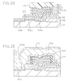
- a field oxide film 202 is formed on the surface of a p-type silicon substrate 201, and an MOS transistor consisting of a gate electrode 203 connected to a word line on a gate oxide film 202a, an n-type node diffused layer 204a, and an n-type bit diffused layer 204b is formed.
- a first interlayer insulating film 205 is deposited all over the surface. At least the surface of the interlayer insulating film 205 is formed of a silicon nitride film.
- a silicon oxide film 227, a first n-type polycrystalline silicon film 213, and a silicon oxide film 228 are formed sequentially (FIG. 1A).
- a photoresist film 218 is formed which has an opening at the position where a node contact hole is to be created, and a node contact hole 206a which reaches the node diffused layer 204a is opened by etching sequentially the silicon oxide film 228, the polycrystalline silicon film 213, the silicon oxide film 227, and the interlayer insulating film 205.
- the silicon oxide film 228, the polycrystalline silicon film 213, and the silicon oxide film 227 become a silicon oxide film 228a, a polycrystalline silicon film 213a, and a silicon oxide film 227a, respectively (FIG. 1B).
- the photoresist film 218 is removed, and a second n-type polycrystalline silicon film is formed all over the surface.
- a photoresist film 219 is formed in the region where a node electrode is to be formed, and the second n-type polycrystalline silicon film, the silicon oxide film 228a, the polycrystalline silicon film 213a and the silicon oxide film 227a are sequentially etched by an anisotropic etching such as RIE (reactive ion etching) that uses the photoresist film 219 as the mask.
- RIE reactive ion etching
- the second n-type polycrystalline silicon film, the silicon oxide film 228a, the polycrystalline silicon film 213a, and the silicon oxide film 227a are converted to a polycrystalline silicon film 223a, a silicon oxide film 228b, a polycrystalline silicon film 213b, and a silicon oxide film 227b, respectively (FIG. 1C).
- a capacitor insulating film 207 is deposited all over the surface.
- a third n-type polycrystalline silicon film is formed all over the surface, and a cell plate electrode 208 is formed by etching the third n-type polycrystalline silicon film.
- a stacked type capacitor is formed by removing the capacitor insulating film 207 by etching, using the cell plate electrode 208 as the mask.
- a second interlayer insulating film 209 is deposited all over the surface, and a bit contact hole 206b is opened by sequentially etching the interlayer insulating films 209 and 205 above the bit diffused layer 204b.
- a bit line 210 is formed, completing a DRAM (FIG. 1E).
- the node electrode 217 of fin structure as shown in FIG. 1D has a sufficiently large surface area.
- the mechanical strength of the node electrode 217 is deteriorated, making the process such as washing extremely difficult.
- FIGs. 2A to 2E are schematic sectional views arranged in order illustrating the method of manufacture of the preferred semiconductor memory device embodying the present invention.
- an active region and an element isolation region are partitioned by forming a field oxide film 102 on the surface of a p-type silicon substrate 101.
- a gate electrode 103 serving also as a word line is formed.
- An n-type node diffused layer 104a and a bit diffused layer 104b are formed on the surface of the active region by using the gate electrode 103 on the active region as the mask, completing a MOS transistor of a DRAM.
- a first interlayer insulating film 105 consisting of a silicon oxide film with thickness of, for example, about 300 nm is formed allover the surface.
- the interlayer insulating film 105 does not need to have its surface formed of a silicon nitride film, as is the case in the known device.
- the structure shown in FIG. 2A is obtained by opening a node contact hole 106a by etching the interlayer insulating film 105 on the node diffused layer 104a.
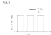
- an undoped polycrystalline silicon film 111 with thickness of, for example, about 150 nm is deposited by thermal decomposition of silane (SiH4) within the temperature range of 500 to 600°C in an LPCVD apparatus.
- an oxygen-rich undoped polycrystalline silicon film 112 is formed by exposing the sample to an argon atmosphere containing 0.2 to 5% of oxygen (O2) in the same apparatus.
- an undoped polycrystalline silicon film 121, an oxygen-rich undoped polycrystalline silicon film 122, a undoped polycrystalline silicon film 131, and an oxygen-rich undoped polycrystalline silicon film 132 are formed sequentially to form a stacked polycrystalline silicon film, obtaining the structure as shown in FIG. 2B.
- the flow rate of silane and argon diluting oxygen are changed periodically as shown, for example, in FIG. 3.
- the film thicknesses of the oxygen-rich undoped polycrystalline silicon films 112, 122, and 132 formed on the surfaces of the undoped polycrystalline silicon films 111, 121, and 131, respectively, are determined by the temperature, pressure, and oxygen partial pressure within the LPCVD apparatus, duration of the operation, and the like, but they are considered to be the thicknesses corresponding to silicon layers with one to several atomic layers. At this time, it is considered that the bonding between oxygen and silicon does not form the complete structure of silicon dioxide (SiO2).
- the sample is taken out of the LPCVD apparatus and is subjected to diffusion by phosphoryl trichloride (POCl3) bubbling at 800 to 850°C to diffuse phosphorus into the stacked film and convert the undoped polycrystalline silicon films 111, 121, and 131 and the oxygen-rich undoped polycrystalline silicon films 112, 122, and 132 to n-type semiconductor films.
- POCl3 phosphoryl trichloride
- the thickness of the oxygen-rich n-type polycrystalline silicon film is 5 to 200 nm, and the sheet resistance of the film is 200 to 1000 ⁇ / ⁇ or so.
- the reason for this is considered to be due to dispersion, in broader manner into the silicon crystals, of oxygen contained in the oxygen-rich undoped polycrystalline silicon film instead of forming the oxide of silicon, as a result of diffusion of phosphorus and the accompanying heat treatment.
- the depth profile of the oxygen concentration is as shown in FIG. 4.
- This result represents a measurement by secondary ion mass spectrometry (SIMS).
- SIMS secondary ion mass spectrometry
- the oxygen concentration has three peaks; a first peak on the surface, a second peak at a depth of about 150 nm, and a third peak at a depth of about 300 nm.
- the second and the third peaks have a considerable spectral width, and the maximum oxygen concentrations at these peaks are about one order of magnitude smaller than the oxygen concentration of a silicon oxide film.
- the first peak is in the state of superposition of a region of extremely high oxygen concentration (about 5 x 101 atoms/cm3 which is comparable to the oxygen concentration of the interlayer insulating film) in a very narrow range, and a region which is the same order as those of the second and the third peaks.
- the region of the first peak with extremely high oxygen concentration corresponds to the region of natural oxide formed on the surface of the stacked film.
- a photoresist film 119 is formed in the region reserved for a node electrode, and anisotropic etching is applied to the stacked film consisting of the n-type polycrystalline silicon using the photoresist film as a mask.
- a stacked film consisting of an oxygen-rich n-type polycrystalline silicon film 134b, an n-type polycrystalline silicon film 133b, an oxygen-rich n-type polycrystalline silicon film 124b, an n-type polycrystalline silicon film 123b, an oxygen-rich n-type polycrystalline silicon film 114b, and an n-type polycrystalline silicon film 113b, as shown in FIG. 2C.
- the side faces of the stacked film are approximately flat.
- the anisotropic etching is an RIE that uses dichlorodifluoromethane (CCl2F2) of about 40 sccm as the etchant gas, carried out under a pressure of about 200 m Torr and an RF power of about 300 W.
- Cl2F2 dichlorodifluoromethane
- isotropic etching is applied,without removal of the photoresist film 119, to the surfaces of the stacked film exposed by the anisotropic etching, by using sulfur hexafluoride (SF6) as the etchant gas.
- SF6 sulfur hexafluoride
- the oxygen-rich n-type polycrystalline silicon film 134b, the n-type polycrystalline silicon film 133b, the oxygen-rich n-type polycrystalline silicon film 124b, the n-type polycrystalline silicon film 123b, the oxygen-rich n-type polycrystalline silicon film 114b, and the n-type polycrystalline silicon film 113b are converted respectively to an oxygen-rich n-type polycrystalline silicon film 134c, an n-type polycrystalline silicon film 133c, an oxygen-rich n-type polycrystalline silicon film 124c, an n-type polycrystalline silicon film 123c, an oxygen-rich n-type polycrystalline silicon film 114c, and an n-type polycrystalline silicon film 113c
- the isotropic etching employed here is carried out, for example, using sulfur hexafluoride of 60 sccm as the etchant gas and helium (He) of 100 sccm as the carrier gas, under a pressure of 400 m Torr and an RF power of 400 W.
- the indentations in this case are about 0.1 to 0.3 ⁇ m.
- the increase in the surface area of the node electrode 117a due to individual indentation is small, for example, even if the increase in the surface area due to a single indentation is about 6%, the surface area of the node electrode can be increased by increasing the number of layers of the oxygen-rich polycrystalline films, as shown in FIG. 5.
- the number of layers of the n-type polycrystalline silicon films that do not contain oxygen (or are oxygen-poor) is three, and the thickness of each film is about 150 nm, so that the increase in the surface area of the node electrode is about 18%.
- the increase in the surface area of the node electrode can be made about 60%.
- a dieletric capacitor insulating film 107 and a cell plate electrode 108 are formed, completing a stacked capacitor.
- a second interlayer insulating film 109 is deposited all over the surface, and a bit contact hole 106b is opened by sequentially etching the interlayer insulating films 109 and 105 on the bit diffused layer 104b.
- a bit line 110 is formed to complete a DRAM which is equipped with the node electrode 117a of the first embodiment as shown in FIG. 2E.
- the present embodiment makes it possible to obtain the fin structure in a smaller number of steps of one photolithography operation (and two etching operations) compared with the method of Figs 1A to 1E. Furthermore, the depth of the indentation of the fins is about 0.3 ⁇ m at the most so that the mechanical strength at the stage of formation of the node electrode can be secured. Moreover, as described above, the number of indentations on the side faces of the node electrode can readily be increased, so that it is easy to obtain a capacitor having large capacitance even if the occupancy area of the stacked capacitor has to be decreased.
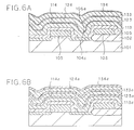
- FIGs. 6A and 6B are schematic sectional views illustrating an alternative method of manufacturing the semiconductor memory device, which is the same as that of the main embodiment up to the process shown in FIG. 2A.
- an oxygen-rich n-type polycrystalline silicon film 114 is formed on the surface of the polycrystalline silicon film 113 by exposing the sample to an argon atmosphere containing 0.2 to 5% of oxygen (O2) within the same apparatus.
- an n-type polycrystalline silicon film 123, an oxygen-rich n-type polycrystalline silicon film 124, an n-type polycrystalline silicon film 133, and an oxygen-rich n-type polycrystalline silicon film 134 are formed sequentially to form a stacked polycrystalline silicon film, obtaining the structure as shown in FIG. 6A.
- the oxygen-rich n-type polycrystalline silicon film 134, the n-type polycrystalline silicon film 133, the oxygen-rich n-type polycrystalline silicon film 124, the n-type polycrystalline silicon film 123, the oxygen-rich n-type polycrystalline silicon film 114, and the n-type polycrystalline silicon film 113 are respectively converted to an oxygen-rich n-type polycrystalline silicon film 134a, an n-type polycrystalline silicon film 133a, an oxygen-rich n-type polycrystalline silicon film 124a, an n-type polycrystalline silicon film 123a, an oxygen-rich n-type polycrystalline silicon film 114a, and an n-type polycrystalline silicon film 113a, as shown in FIG.
- the purpose of the heat treatment is to disperse oxygen in, for example, the oxygen-rich n-type polycrystalline silicon film 114, and as a result, the thickness of the oxygen-rich n-type polycrystalline silicon film 114a is increased relative to the thickness of the oxygen-rich n-type polycrystalline silicon film 114.
- a node electrode is completed through processes similar to those shown in FIGs. 2C and 2D. Further, a DRAM equipped with the node electrode is completed by the same manufacturing method as shown in FIG. 2E.
- a stacked film is formed consisting of polycrystalline silicon films which are n-type from the beginning.
- the growth rate of the n-type polycrystalline silicon film by the above-mentioned method is smaller than the growth rate of the undoped polycrystalline silicon film of FIGs. 2A to 2E.
- the thickness of the oxygen-rich n-type polycrystalline silicon film 114a depends on the conditions of the heat treatment. Therefore, the thickness of the n-type polycrystalline silicon film 113a and the oxygen-rich n-type polycrystalline silicon film 114a, for example, can further be reduced compared with the main embodiment.
- the alternative method makes it possible to further increase the surface area of the side faces of the node electrode.
- the stacked film consisting of the polycrystalline silicon films were made by an LPCVD method.
Landscapes
- Engineering & Computer Science (AREA)
- Manufacturing & Machinery (AREA)
- Semiconductor Memories (AREA)
Claims (5)
- Mémoire vive dynamique comprenant un transistor MOS comportant une électrode de grille (103), une couche diffusée de noeud (104a) et une couche diffusée de bit (104b) et un condensateur comportant une électrode de noeud (117a) connectée à la couche diffusée de noeud, un film diélectrique (107) formé sur l'électrode de noeud et une électrode de plaque de cellule (108) formée sur la couche diélectrique, dans laquelle l'électrode de noeud est constituée par un premier film en silicium polycristallin de type n (113c, 123c, 133c) empilé en alternance avec un second film en silicium polycristallin de type n (114b, 124b, 134b), le second film en silicium polycristallin présentant une teneur en oxygène supérieure à celle du premier film en silicium polycristallin, et dans laquelle la partie d'extrémité de chaque premier film polycristallin est en une position davantage enfoncée que la partie d'extrémité de chaque dit second film polycristallin.
- Procédé de fabrication d'une électrode de noeud d'une mémoire vive dynamique incluant un transistor MOS et un condensateur empilé, comprenant les étapes de :formation d'un transistor MOS constitué par une électrode de grille qui joue le rôle de ligne de mot sur un film d'isolation de grille et par une couche diffusée de noeud de type n et une couche diffusée de bit de type n qui sont formées sur unc surface d'un substrat en silicium de type p, dépôt d'un film isolant intercouche sur la totalité de la surface et ouverture d'un trou de contact de noeud qui atteint la couche diffusée de noeud dans le film isolant intercouche ;formation d'un film empilé en déposant en alternance un premier film en silicium polycristallin de type n et un second film en silicium polycristallin de type n, le second film en silicium polycristallin présentant une teneur en oxygène supérieure à celle du premier film en silicium polycristallin, d'où une vitesse de gravure plus lente ;formation d'un film de photoréserve dans une région pour former une électrode de noeud et gravure anisotrope du film empilé en utilisant le film de photoréserve en tant que masque ; etgravure isotrope d'au moins la surface du film empilé qui est mise à nu par la gravure anisotrope.
- Procédé de fabrication d'un dispositif de mémoire à semiconducteur selon la revendication 2, dans lequel l'étape de formation du film empilé comprend la mise en oeuvre d'un dépôt alterné d'un film en silicium polycristallin non dopé et la formation d'un film en silicium polycristallin non dopé riche en oxygène sur la surface du film en silicium polycristallin non dopé en exposant le film en silicium polycristallin non dopé à une atmosphère d'oxygène et en formant un premier film empilé constitué par ledit film en silicium polycristallin non dopé et par ledit film en silicium polycristallin non dopé riche en oxygène, et la diffusion de phosphore dans le premier film empilé.
- Procédé de fabrication d'un dispositif de mémoire à semiconducteur selon la revendication 2, dans lequel l'étape de formation du film empilé comprend la mise en oeuvre d'un dépôt alterné du premier film en silicium polycristallin de type n au moyen d'un procédé de dépôt chimique en phase vapeur (CVD) qui utilise du gaz silane comprenant de la phosphine, et la formation du second film en silicium polycristallin de type n sur la surface du premier film en silicium polycristallin de type n en exposant le premier film en silicium polycristallin de type n à de l'oxygène et en mettant en oeuvre un traitement thermique dans une atmosphère inerte.
- Procédé de fabrication d'un dispositif de mémoire à semiconducteur selon la revendication 4, dans lequel la gravure isotrope est une gravure par voie sèche qui utilise un gaz de gravure qui contient au moins de l'hexafluorure de souffre.
Applications Claiming Priority (4)
| Application Number | Priority Date | Filing Date | Title |
|---|---|---|---|
| JP29153890 | 1990-10-29 | ||
| JP291538/90 | 1990-10-29 | ||
| JP03041474A JP3104262B2 (ja) | 1991-03-07 | 1991-03-07 | 半導体装置およびその製造方法 |
| JP41474/91 | 1991-03-07 |
Publications (2)
| Publication Number | Publication Date |
|---|---|
| EP0484088A1 EP0484088A1 (fr) | 1992-05-06 |
| EP0484088B1 true EP0484088B1 (fr) | 1996-05-08 |
Family
ID=26381099
Family Applications (1)
| Application Number | Title | Priority Date | Filing Date |
|---|---|---|---|
| EP91309956A Expired - Lifetime EP0484088B1 (fr) | 1990-10-29 | 1991-10-29 | Cellule DRAM à condensateur empilé |
Country Status (4)
| Country | Link |
|---|---|
| US (2) | US5504704A (fr) |
| EP (1) | EP0484088B1 (fr) |
| KR (1) | KR960016837B1 (fr) |
| DE (1) | DE69119354T2 (fr) |
Families Citing this family (32)
| Publication number | Priority date | Publication date | Assignee | Title |
|---|---|---|---|---|
| JP2542706B2 (ja) * | 1989-10-05 | 1996-10-09 | 株式会社東芝 | ダイナミックram |
| JPH05198768A (ja) * | 1992-01-21 | 1993-08-06 | Mitsubishi Electric Corp | 半導体記憶装置およびその製造方法 |
| JPH0621018A (ja) * | 1992-06-29 | 1994-01-28 | Sony Corp | ドライエッチング方法 |
| KR960003771B1 (ko) * | 1992-08-08 | 1996-03-22 | 삼성전자주식회사 | 반도체 메모리장치 |
| US5436186A (en) * | 1994-04-22 | 1995-07-25 | United Microelectronics Corporation | Process for fabricating a stacked capacitor |
| KR0136533B1 (ko) * | 1994-06-09 | 1998-09-15 | 문정환 | 불휘발성 반도체 메모리 소자 및 그의 제조방법 |
| KR960006030A (ko) * | 1994-07-18 | 1996-02-23 | 김주용 | 반도체소자의 캐패시터 제조방법 |
| JPH0831174A (ja) * | 1994-07-18 | 1996-02-02 | Fujitsu Ltd | 半導体記憶装置 |
| US5538592A (en) * | 1994-07-22 | 1996-07-23 | International Business Machines Corporation | Non-random sub-lithography vertical stack capacitor |
| US5564180A (en) * | 1994-11-14 | 1996-10-15 | United Microelectronics Corp. | Method of fabricating DRAM cell capacitor |
| KR0155785B1 (ko) * | 1994-12-15 | 1998-10-15 | 김광호 | 핀형 커패시터 및 그 제조방법 |
| US5672535A (en) * | 1995-05-31 | 1997-09-30 | Alliance Semiconductor Corporation | Method of fabricating DRAM cell with self-aligned contact |
| DE19527023C1 (de) * | 1995-07-24 | 1997-02-27 | Siemens Ag | Verfahren zur Herstellung eines Kondensators in einer Halbleiteranordnung |
| US5701264A (en) * | 1995-12-13 | 1997-12-23 | Alliance Semiconductor Corporation | Dynamic random access memory cell having increased capacitance |
| US5792708A (en) * | 1996-03-06 | 1998-08-11 | Chartered Semiconductor Manufacturing Pte Ltd. | Method for forming residue free patterned polysilicon layers upon high step height integrated circuit substrates |
| US5591664A (en) * | 1996-03-20 | 1997-01-07 | Taiwan Semiconductor Manufacturing Company Ltd. | Method of increasing the capacitance area in DRAM stacked capacitors using a simplified process |
| US5994730A (en) | 1996-11-21 | 1999-11-30 | Alliance Semiconductor Corporation | DRAM cell having storage capacitor contact self-aligned to bit lines and word lines |
| TW311258B (en) * | 1997-01-24 | 1997-07-21 | United Microelectronics Corp | Manufacturing method of stack capacitor of dynamic random access memory |
| JP3373134B2 (ja) * | 1997-06-13 | 2003-02-04 | 沖電気工業株式会社 | 半導体装置の製造方法 |
| US5970358A (en) * | 1997-06-30 | 1999-10-19 | Micron Technology, Inc. | Method for forming a capacitor wherein the first capacitor plate includes electrically coupled conductive layers separated by an intervening insulative layer |
| US5903493A (en) * | 1997-09-17 | 1999-05-11 | Lucent Technologies Inc. | Metal to metal capacitor apparatus and method for making |
| US6329703B1 (en) * | 1998-02-25 | 2001-12-11 | Infineon Technologies Ag | Contact between a monocrystalline silicon region and a polycrystalline silicon structure and method for producing such a contact |
| US6210813B1 (en) * | 1998-09-02 | 2001-04-03 | Micron Technology, Inc. | Forming metal silicide resistant to subsequent thermal processing |
| KR100311498B1 (ko) | 1999-01-12 | 2001-11-02 | 김영환 | 반도체 소자의 이중 게이트 형성방법 |
| KR100313510B1 (ko) | 1999-04-02 | 2001-11-07 | 김영환 | 반도체 소자의 제조방법 |
| WO2002080244A2 (fr) | 2001-02-12 | 2002-10-10 | Asm America, Inc. | Procede ameliore permettant de deposer des films semi-conducteurs |
| US7320131B1 (en) * | 2001-06-06 | 2008-01-15 | Cisco Technology, Inc. | Methods and apparatus for selecting a server to process a request |
| US7186630B2 (en) * | 2002-08-14 | 2007-03-06 | Asm America, Inc. | Deposition of amorphous silicon-containing films |
| US6746877B1 (en) * | 2003-01-07 | 2004-06-08 | Infineon Ag | Encapsulation of ferroelectric capacitors |
| US7005160B2 (en) * | 2003-04-24 | 2006-02-28 | Asm America, Inc. | Methods for depositing polycrystalline films with engineered grain structures |
| US8629063B2 (en) * | 2011-06-08 | 2014-01-14 | International Business Machines Corporation | Forming features on a substrate having varying feature densities |
| US9048212B2 (en) * | 2012-05-15 | 2015-06-02 | Taiwan Semiconductor Manufacturing Company, Ltd. | Semiconductor devices, methods of manufacture thereof, and methods of manufacturing capacitors |
Family Cites Families (6)
| Publication number | Priority date | Publication date | Assignee | Title |
|---|---|---|---|---|
| JPH0682783B2 (ja) * | 1985-03-29 | 1994-10-19 | 三菱電機株式会社 | 容量およびその製造方法 |
| DE3856143T2 (de) * | 1987-06-17 | 1998-10-29 | Fujitsu Ltd | Verfahren zum Herstellen einer dynamischen Speicherzelle mit wahlfreiem Zugriff |
| US4901043A (en) * | 1987-07-02 | 1990-02-13 | Andrew F. Tresness | Compact filter having a multi-compartment housing |
| JPS6420050A (en) * | 1987-07-14 | 1989-01-24 | Maruka Kk | Production of boneless fish |
| JPH01120050A (ja) * | 1987-11-02 | 1989-05-12 | Hitachi Ltd | 半導体記憶装置 |
| JPH0210762A (ja) * | 1988-06-28 | 1990-01-16 | Mitsubishi Electric Corp | キャパシタ |
-
1991
- 1991-10-29 DE DE69119354T patent/DE69119354T2/de not_active Expired - Fee Related
- 1991-10-29 EP EP91309956A patent/EP0484088B1/fr not_active Expired - Lifetime
- 1991-10-29 KR KR91019264A patent/KR960016837B1/ko not_active IP Right Cessation
- 1991-10-29 US US07/784,269 patent/US5504704A/en not_active Expired - Lifetime
-
1994
- 1994-09-01 US US08/299,885 patent/US5416037A/en not_active Expired - Lifetime
Also Published As
| Publication number | Publication date |
|---|---|
| US5416037A (en) | 1995-05-16 |
| DE69119354T2 (de) | 1996-09-19 |
| KR960016837B1 (en) | 1996-12-21 |
| EP0484088A1 (fr) | 1992-05-06 |
| US5504704A (en) | 1996-04-02 |
| DE69119354D1 (de) | 1996-06-13 |
Similar Documents
| Publication | Publication Date | Title |
|---|---|---|
| EP0484088B1 (fr) | Cellule DRAM à condensateur empilé | |
| EP0264858B1 (fr) | Cellule de mémoire du type RAM comprenant un condensateur de stockage commun dans un sillon, dont les parois déterminent les contacts à pont et les électrodes de porte | |
| US5384276A (en) | Method of fabricating a memory device with a multilayer insulating film | |
| KR960005245B1 (ko) | 반도체장치의 제조방법 | |
| US5696395A (en) | Dynamic random access memory with fin-type stacked capacitor | |
| EP0317199A2 (fr) | Structures de couches pour cellule à mémoire pour dispositif de mémoire dynamique à accès aléatoire et procédé pour sa fabrication | |
| US4692994A (en) | Process for manufacturing semiconductor devices containing microbridges | |
| US4826781A (en) | Semiconductor device and method of preparation | |
| GB2244861A (en) | Integrated circuit capacitor | |
| JP2817645B2 (ja) | 半導体装置の製造方法 | |
| KR0151196B1 (ko) | 반도체 메모리장치의 제조방법 | |
| US20010044182A1 (en) | Semiconductor device having hsg polycrystalline silicon layer | |
| JP3038088B2 (ja) | 半導体記憶装置の製造方法 | |
| JP3020257B2 (ja) | 半導体記憶装置の製造方法 | |
| JPH0621393A (ja) | 半導体メモリー装置の製造方法 | |
| JPH02143456A (ja) | 積層型メモリセルの製造方法 | |
| JP3067329B2 (ja) | 半導体記憶装置およびその製造方法 | |
| JPS6315749B2 (fr) | ||
| JPS6185857A (ja) | 半導体メモリ素子の製造方法 | |
| JPS61225851A (ja) | 半導体装置及びその製造方法 | |
| JPH0734451B2 (ja) | 半導体装置の製造方法 | |
| JP2903191B2 (ja) | 半導体装置の製造方法 | |
| JPH022672A (ja) | 半導体メモリセルとその製造方法 | |
| KR930004724B1 (ko) | 다층 스택 캐패시터의 제조방법 및 그에 따른 캐패시터 | |
| JP2833338B2 (ja) | 半導体装置の製造方法 |
Legal Events
| Date | Code | Title | Description |
|---|---|---|---|
| PUAI | Public reference made under article 153(3) epc to a published international application that has entered the european phase |
Free format text: ORIGINAL CODE: 0009012 |
|
| 17P | Request for examination filed |
Effective date: 19911119 |
|
| AK | Designated contracting states |
Kind code of ref document: A1 Designated state(s): DE FR GB |
|
| 17Q | First examination report despatched |
Effective date: 19940315 |
|
| GRAH | Despatch of communication of intention to grant a patent |
Free format text: ORIGINAL CODE: EPIDOS IGRA |
|
| GRAA | (expected) grant |
Free format text: ORIGINAL CODE: 0009210 |
|
| AK | Designated contracting states |
Kind code of ref document: B1 Designated state(s): DE FR GB |
|
| REF | Corresponds to: |
Ref document number: 69119354 Country of ref document: DE Date of ref document: 19960613 |
|
| ET | Fr: translation filed | ||
| PLBE | No opposition filed within time limit |
Free format text: ORIGINAL CODE: 0009261 |
|
| STAA | Information on the status of an ep patent application or granted ep patent |
Free format text: STATUS: NO OPPOSITION FILED WITHIN TIME LIMIT |
|
| 26N | No opposition filed | ||
| REG | Reference to a national code |
Ref country code: GB Ref legal event code: IF02 |
|
| REG | Reference to a national code |
Ref country code: GB Ref legal event code: 732E |
|
| REG | Reference to a national code |
Ref country code: FR Ref legal event code: TQ |
|
| REG | Reference to a national code |
Ref country code: GB Ref legal event code: 732E |
|
| REG | Reference to a national code |
Ref country code: FR Ref legal event code: TP Ref country code: FR Ref legal event code: TQ |
|
| PGFP | Annual fee paid to national office [announced via postgrant information from national office to epo] |
Ref country code: GB Payment date: 20061025 Year of fee payment: 16 |
|
| PGFP | Annual fee paid to national office [announced via postgrant information from national office to epo] |
Ref country code: DE Payment date: 20061026 Year of fee payment: 16 |
|
| GBPC | Gb: european patent ceased through non-payment of renewal fee |
Effective date: 20071029 |
|
| PG25 | Lapsed in a contracting state [announced via postgrant information from national office to epo] |
Ref country code: DE Free format text: LAPSE BECAUSE OF NON-PAYMENT OF DUE FEES Effective date: 20080501 |
|
| REG | Reference to a national code |
Ref country code: FR Ref legal event code: ST Effective date: 20080630 |
|
| PGFP | Annual fee paid to national office [announced via postgrant information from national office to epo] |
Ref country code: FR Payment date: 20061010 Year of fee payment: 16 |
|
| PG25 | Lapsed in a contracting state [announced via postgrant information from national office to epo] |
Ref country code: GB Free format text: LAPSE BECAUSE OF NON-PAYMENT OF DUE FEES Effective date: 20071029 |
|
| PG25 | Lapsed in a contracting state [announced via postgrant information from national office to epo] |
Ref country code: FR Free format text: LAPSE BECAUSE OF NON-PAYMENT OF DUE FEES Effective date: 20071031 |