EP0483846B1 - Analog-Digitalwandlerschaltung - Google Patents
Analog-Digitalwandlerschaltung Download PDFInfo
- Publication number
- EP0483846B1 EP0483846B1 EP91118616A EP91118616A EP0483846B1 EP 0483846 B1 EP0483846 B1 EP 0483846B1 EP 91118616 A EP91118616 A EP 91118616A EP 91118616 A EP91118616 A EP 91118616A EP 0483846 B1 EP0483846 B1 EP 0483846B1
- Authority
- EP
- European Patent Office
- Prior art keywords
- bias voltage
- voltage
- offset
- converter
- analog signal
- Prior art date
- Legal status (The legal status is an assumption and is not a legal conclusion. Google has not performed a legal analysis and makes no representation as to the accuracy of the status listed.)
- Expired - Lifetime
Links
Images


Classifications
-
- H—ELECTRICITY
- H03—ELECTRONIC CIRCUITRY
- H03M—CODING; DECODING; CODE CONVERSION IN GENERAL
- H03M1/00—Analogue/digital conversion; Digital/analogue conversion
- H03M1/06—Continuously compensating for, or preventing, undesired influence of physical parameters
- H03M1/0602—Continuously compensating for, or preventing, undesired influence of physical parameters of deviations from the desired transfer characteristic
- H03M1/0604—Continuously compensating for, or preventing, undesired influence of physical parameters of deviations from the desired transfer characteristic at one point, i.e. by adjusting a single reference value, e.g. bias or gain error
- H03M1/0607—Offset or drift compensation
-
- H—ELECTRICITY
- H03—ELECTRONIC CIRCUITRY
- H03M—CODING; DECODING; CODE CONVERSION IN GENERAL
- H03M1/00—Analogue/digital conversion; Digital/analogue conversion
- H03M1/12—Analogue/digital converters
Definitions
- the present invention relates to an analog-to-digital (A/D) converter circuit, more specifically to an A/D converter circuit capable of removing an offset in an input of an analog signal.
- A/D analog-to-digital
- a conventional A/D converter circuit for efficiently performing analog to digital conversion by biasing the input signal level by a predetermined level is constructed as illustrated in FIG. 9. That is, the analog signal applied to an analog signal input terminal 1 is first applied to a bias voltage summing circuit 2 in which a bias voltage from a bias voltage generation circuit 3 is summed with the analog signal before being applied to the A/D converter circuit 4.
- the A/D converter circuit 4 is provided with a high potential reference voltage input terminal 5 and a low potential reference voltage input terminal 6 for quantizing the analog signal in the voltage range from the low potential reference voltage to the high potential reference voltage. If the number of quantization bits is, for example, 8 bits, the output from the A/D converter circuit will be OOH when the input is equal to the low potential reference voltage. On the other hand, the output will be FFH when the input is equal to the high potential reference voltage.
- the A/D converter 4 may be operated with a single or a dual voltage source. The following conditions must be met between the reference voltage and the power supply voltages: voltage of the negative voltage source ⁇ low potential reference voltage ⁇ high potential reference voltage ⁇ voltage of the positive voltage source.
- a bias voltage is added by the bias voltage summing circuit 2 to shift the input signal voltage varying from 0 volt to the high potential reference voltage before analog to digital conversion.
- summed with the input analog signal is one-half of the high potential reference voltage as the bias voltage, thereby outputting 80H from the A/D converter when 0 volt input is applied to the bias voltage summing circuit.
- the conventional A/D converter circuit described above has a problem to cause offset in the output of the A/D converter.
- a voltage divider circuit to divide the reference voltage may be used for obtaining the bias voltage.
- it is difficult to obtain a desirec resistance ratio because of tolerance of resistors. Setting a desired resistance ratio using a variable resistor or a potentiometer is not stable enough due to aging, temperature variation, etc. Accordingly, the bias voltage may be subjected to considerable changes due to aging, temperature variation, accuracy of parts, etc.
- US-A-4,907,165 discloses an electric energy measuring method which corrects the offsets in an A/D converter by an average value of accumulated digital values during sampling.
- US-A-4,942,399 discloses an adaptive flash A/D converter for a differential input signal; the average value of the level-shifted and converted signal is compared with the midpoint of a set of reference voltages in order to generate a control signal for the converted signal.
- any offset from the ideal value of the average voltage in the input signal to the A/D converter circuit is detected by an offset detection circuit.
- the detected offset is subtracted from the digital output data from the A/D converter to compensate the digital output data by removing the offset in the analog signal and the bias voltage from the output data from the A/D converter.
- the bias voltage is modified by the detected offset voltage of the offset detection circuit in such a manner that the average voltage in the input signal to the A/D converter is equal to the ideal voltage, thereby not causing any offset in the output from the A/D converter.
- the modification of the bias voltage means that the bias voltage is made to be equal to the ideal bias voltage and that the offset voltage in the analog signal is canceled.
- FIG. 1 Illustrated in FIG. 1 is a block diagram of a first embodiment of the A/D converter circuit according to the present invention in which like reference numerals are used to represent elements similar to those in FIG. 9.
- a first embodiment features the addition of a subtractor 7 and an offset detection circuit 8.
- the analog signal to be applied to an input analog signal input terminal 1 has a known average voltage but is offset as described above. Samples of the input signal will be equally distributed on both sides of the average voltage in case of Gaussian distribution or uniform distribution. Examples of such input signals are sinusoidal waveform signals and eye pattern signals obtained by orthogonal demodulation of MSK or QPSK modulation signals. An example of asymmetrical distribution is a signal due to the electric field fluctuation under, for example, Rayleigh fading. Also, an error is contained in the bias voltage generated by a bias voltage generator circuit 3.
- V AD V AV + ⁇ V + V B + ⁇ V B
- V AD ' V AV + V B
- An offset detection circuit 8 has two terminals 9 and 10 for externally receiving the ideal value of the bias voltage and the ideal average voltage of the analog signal, respectively. Firstly, output samples from the A/D converter 4 are used to obtain the average voltage of the analog signal which is given by the above expression (1). Then, the offset ( ⁇ V + ⁇ V B ) is detected through mathematical operation by subtracting the ideal average of the analog signal to be applied to the ideal average voltage input terminal 10 and the ideal bias voltage to be applied to the bias voltage input terminal 9 from the obtained average voltage, i.e., subtracting the above expression (2) from the expression (1).
- a subtractor 7 subtracts the output data of the offset detection circuit 8 from the output data of the A/D converter 4. This results in providing from a digital data output terminal 11 a correct digital output data in which the offset ⁇ V in the analog signal and the offset ⁇ V B in the bias voltage are removed.
- Illustrated in FIG. 2(a) is an original waveform of the analog signal free from any offset.
- the offset detection circuit 8 and the subtractor 7 are constructed by a processing circuit to perform the series of processing the sample data from the A/D converter 4 as illustrated in FIG. 3.
- An offset voltage D OFFSET is obtained (or assumed) by subtracting the sum D' AD of the ideal average voltage of the input analog signal and the ideal bias voltage respectively applied to the terminals 9 and 10 from the average value D AD (in step S7).
- the corrected data D'(k) is derived from an output terminal 11 (in step S10). A judgement is made if K reached (N-1) (in step S11).
- step S11 K is incremented by 1 if (N-1) is not reached yet (in step S12) to return to step S9.
- step S11 the correction of the above N samples is finished.
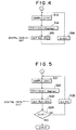
- the correction of the subsequent (N+1)-th sample is carried out in the same manner as the steps S9 and S10. Processing procedures for correction of an unlimited number of subsequent samples are illustrated in FIG. 4.
- sample value D(k) is obtained (in step S13)
- the corrected date D'(k) is obtained by subtracting the offset voltage D OFFSET from the above D(k) (in step S14)
- the corrected data D'(k) is derived from the output terminal 11 (in step S15).
- K is incremented by 1 (in step S16) to perform the similar processing on the subsequent samples by returning to step S13.
- FIG. 5 is an example of performing correction only on predetermined number (N') of samples D(N+1), D(N+2), ..., D(N+N') after completing the processing step S11 in FIG. 3.
- the sample D(k) is obtained in step S21 and the corrected data D'(k) is obtained by subtracting the offset voltage D OFFSET from the above D(k) (in step S22).
- a judgement is made if K reaches (N'-1) (in step S24). If (N'-1) is not reached, K is incremented by 1 (in step S25) to return step S21. Processing is terminated if K reaches (N'-1). It is a matter of course that the offset detection using the sample value obtained from the A/D converter 4 and the correction of the output data from the A/D converter can be made after temporarily storing the data in a memory or the like.
- FIG. 6 illustrates the A/D converter circuit according to a second embodiment of the present invention.
- the second embodiment eliminates the subtractor 7 in the first embodiment.
- the digital output (D OFFSET ) from the offset detection circuit 8 is converted into an analog signal by a D/A (digital-to-analog) converter 12 and is applied to a bias voltage summing circuit 2' so that the average voltage of the input signal to the A/D converter 4 is equal to the voltage as given by the above expression (2).
- D/A digital-to-analog
- the bias voltage summing circuit 2' is provided with means to correct the input analog signal to cancel the offset voltage so that the input bias voltage is equal to the ideal bias voltage.
- an offset free correct digital data is derived from the A/D converter 4.
- the offset voltage D OFFSET derived from the offset detection circuit 8 is converted into an analog signal by a D/A converter 13 before being applied to the bias voltage generation circuit 3 for previously correcting the bias voltage by the bias voltage generation circuit 3 as illustrated in FIG. 7.
- the processing steps S1 through S6 in FIG. 3 are used to determine the offset voltage D OFFSET .
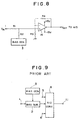
- the bias voltage summing circuit 2 may be implemented, for example, by using an operational amplifier 14 as illustrated in FIG. 8.
- the analog signal to the input terminal 1 in FIG. 8 is applied to the non-inverting input terminal of the operational amplifier 14 by way of a resistor R1.
- the bias voltage from the bias voltage generation circuit 3 is summed by way of a resistor R2.
- the inverting input of the operational amplifier 14 is returned to ground by way of a resistor R3 and is connected to the output terminal by way of a feedback resistor R4.
- Two voltage sources +15 V and -15 V are used for operating the operational amplifier 14.
- the A/D converter circuit corrects the output data from the A/D converter for converting the analog signal in the range from the low to the high potential reference voltages into a corresponding digital data by detecting the offset from the ideal value for the bias voltage to be added to the input signal to the A/D converter and the offset from the ideal value of the average voltage in the analog signal.
- an offset from the ideal value of the bias voltage to be added to the input signal to the A/D converter for converting the analog signal in the range from the low to the high potential reference voltages into the corresponding digital data and also the offset from the ideal value of the average voltage in the analog signal are detected to correct the bias voltage so that the average voltage of the input signal to the A/D converter is equal to the ideal value.
- the correct digital data will be effectively obtained.
Claims (3)
- A/D-Wandlerschaltung mit:einer Vorspannungssummiereinrichtung (2, 2') zum Addieren einer Vorspannung auf ein Analogsignal;einer Vorspannungserzeugungseinrichtung (3) zum Erzeugen der Vorspannung;einer A/D-Wandlereinrichtung (4) zum Digitalisieren des von der Vorspannungssummiereinrichtung (2, 2') ausgegebenenAnalogsignals in dem Bereich zwischen einer niedrigen und einer hohen Referenzspannung, gekennzeichnet durch:eine Einrichtung (8) zum Detektieren des Offset spannungswertes durch Subtrahieren des idealen Mittelwertspannungswertes des Analogsignals und des idealen Wertes der Vorspannung von dem Mittelwert; undeine Korrektureinrichtung (13; 12) zum Zuführen des Ausgangssignals der Offsetdetektionseinrichtung (8) entweder zu der Vorspannungserzeugungsschaltung (3) oder der Vorspannungssummiereinrichtung (2, 2'), um die Vorspannung so zu korrigieren, daß die Mittelwertspannung des Eingangssignals zu der A/D-Wandlereinrichtung gleich dem Idealwert ist.
- A/D-Wandlerschaltung nach Anspruch 1 und mit:einer Einrichtung zum Ausgeben des akkumulierten Wertes einer vorbestimmten Anzahl (N) von Abtastwerten; undeiner Einrichtung für den Erhalt des Mittelwertes durch Dividieren des akkumulierten Wertes durch N.
- A/D-Wandlerschaltung nach Anspruch 2, wobei die Korrektureinrichtung aufweist:eine D/A-Wandlereinrichtung (13; 12) zum Umwandeln der erhaltenen Offsetspannung in ein Analogsignal und zum Zuführen des umgewandelten Signals entweder an die Vorspannungserzeugungsschaltung (3) oder an die Vorspannungssummierschaltung (2') ; undeine auf das Ausgangssignal der D/A-Wandlereinrichtung (13; 12) reagierende Einrichtung zum Kompensieren der Vorpannung entweder von der Vorspannungserzeugungsschaltung (3) oder der Vorspannungssummierschaltung (2').
Applications Claiming Priority (2)
| Application Number | Priority Date | Filing Date | Title |
|---|---|---|---|
| JP29762090 | 1990-11-02 | ||
| JP297620/90 | 1990-11-02 |
Publications (3)
| Publication Number | Publication Date |
|---|---|
| EP0483846A2 EP0483846A2 (de) | 1992-05-06 |
| EP0483846A3 EP0483846A3 (en) | 1993-08-11 |
| EP0483846B1 true EP0483846B1 (de) | 1998-07-29 |
Family
ID=17848918
Family Applications (1)
| Application Number | Title | Priority Date | Filing Date |
|---|---|---|---|
| EP91118616A Expired - Lifetime EP0483846B1 (de) | 1990-11-02 | 1991-10-31 | Analog-Digitalwandlerschaltung |
Country Status (8)
| Country | Link |
|---|---|
| US (1) | US5146223A (de) |
| EP (1) | EP0483846B1 (de) |
| JP (1) | JP2924373B2 (de) |
| KR (1) | KR920011086A (de) |
| AU (1) | AU639839B2 (de) |
| CA (1) | CA2054820C (de) |
| DE (1) | DE69129891T2 (de) |
| SG (1) | SG52469A1 (de) |
Families Citing this family (18)
| Publication number | Priority date | Publication date | Assignee | Title |
|---|---|---|---|---|
| US5281968A (en) * | 1991-09-06 | 1994-01-25 | Nec Corporation | DC offset correction circuit for A/D converter |
| US5227794A (en) * | 1991-12-23 | 1993-07-13 | Ford Motor Company | Frequency multiplexed analog-digital conversion |
| US5293166A (en) * | 1992-03-31 | 1994-03-08 | Vlsi Technology, Inc. | Digital-to-analog converter and bias compensator therefor |
| FR2696300B1 (fr) * | 1992-09-25 | 1994-11-18 | Thomson Csf | Circuit de codage analogique-numérique à compensation automatique du décalage du zéro. |
| US5352938A (en) * | 1992-12-14 | 1994-10-04 | Delco Electronics Corporation | Analog to digital signal conversion |
| US5523756A (en) * | 1994-01-18 | 1996-06-04 | The Grass Valley Group, Inc. | Analog-to-digital converter with offset reduction loop |
| EP0707383B1 (de) * | 1994-06-14 | 2002-05-02 | Stage Tec Entwicklungsgesellschaft für professionelle Audiotechnik mbH | Schaltungsanordnung zur Analog-Digital-Wandlung von Signalen |
| US5892472A (en) * | 1997-06-30 | 1999-04-06 | Harris Corporation | Processor controlled analog-to-digital converter circuit |
| JP4488553B2 (ja) * | 1999-07-14 | 2010-06-23 | 株式会社アドバンテスト | 波形取得方法及びこの方法を用いて動作する波形取得装置 |
| JP2003509141A (ja) | 1999-09-11 | 2003-03-11 | 株式会社ソニー・コンピュータエンタテインメント | 操作装置および同装置の信号出力調整方法 |
| DE60307226D1 (de) * | 2003-02-18 | 2006-09-14 | St Microelectronics Srl | Analog-Digital-Wandler mit Korrektur von Verschiebungsfehlern |
| US6784820B1 (en) * | 2003-04-09 | 2004-08-31 | Raytheon Company | High resolution, high dynamic range analog-to-digital converter system and related techniques |
| JP2007233598A (ja) * | 2006-02-28 | 2007-09-13 | Star Micronics Co Ltd | 磁気インク文字読取装置及びその制御方法 |
| KR100743965B1 (ko) * | 2007-05-11 | 2007-08-01 | 쓰리에이로직스(주) | Rf 신호의 오프셋 전압을 보상할 수 있는 복조기 및 그방법 |
| JP2013041631A (ja) * | 2009-12-02 | 2013-02-28 | Panasonic Corp | 信号処理方法、信号処理装置、及び情報記録再生装置 |
| TWI467923B (zh) * | 2012-01-16 | 2015-01-01 | Novatek Microelectronics Corp | 類比到數位轉換電路以及類比到數位轉換方法 |
| JP2014165649A (ja) * | 2013-02-25 | 2014-09-08 | Fujitsu Semiconductor Ltd | アナログデジタル変換装置 |
| CN115469134A (zh) * | 2022-09-08 | 2022-12-13 | 山东浪潮科学研究院有限公司 | 一种自适应宽动态模数转换电路 |
Family Cites Families (19)
| Publication number | Priority date | Publication date | Assignee | Title |
|---|---|---|---|---|
| US3405238A (en) * | 1964-05-06 | 1968-10-08 | Hurvitz Hyman | Means to eliminate redundant information |
| FR2171960B1 (de) * | 1972-02-17 | 1978-03-03 | Labo Cent Telecommunicat | |
| FR2396463A1 (fr) * | 1977-06-30 | 1979-01-26 | Ibm France | Circuit pour compenser les decalages du zero dans les dispositifs analogiques et application de ce circuit a un convertisseur analogique-numerique |
| US4228423A (en) * | 1977-12-30 | 1980-10-14 | The United States Of America As Represented By The Secretary Of The Air Force | Offset correction apparatus for a successive approximation A/D converter |
| US4229703A (en) * | 1979-02-12 | 1980-10-21 | Varian Associates, Inc. | Zero reference and offset compensation circuit |
| JPS57202128A (en) * | 1981-06-08 | 1982-12-10 | Victor Co Of Japan Ltd | Analog-to-digital converting circuit |
| JPS60197016A (ja) * | 1984-03-21 | 1985-10-05 | Toshiba Corp | アナログ・デジタル変換回路装置 |
| JPS6184186A (ja) * | 1984-10-01 | 1986-04-28 | Nec Corp | クランプレベル補正回路 |
| US4590458A (en) * | 1985-03-04 | 1986-05-20 | Exxon Production Research Co. | Offset removal in an analog to digital conversion system |
| JPS61292067A (ja) * | 1985-06-19 | 1986-12-22 | Mitsubishi Electric Corp | 電力量測定方法 |
| JPS62120723A (ja) * | 1985-11-20 | 1987-06-02 | Nec Corp | A/d変換器用バイアス回路 |
| JPS62281618A (ja) * | 1986-05-30 | 1987-12-07 | Anritsu Corp | 直流オフセツト電圧除去回路 |
| JPH0758907B2 (ja) * | 1986-06-07 | 1995-06-21 | ソニー株式会社 | オフセツト自動補正a/d変換回路 |
| US4771267A (en) * | 1986-12-24 | 1988-09-13 | Hughes Aircraft Company | Analog offset compensation technique |
| JPS6416024A (en) * | 1987-07-09 | 1989-01-19 | Matsushita Electric Ind Co Ltd | Offset correction type analog/digital converter |
| JPH0186328U (de) * | 1987-11-26 | 1989-06-07 | ||
| AU623462B2 (en) * | 1989-02-03 | 1992-05-14 | Alcatel Australia Limited | Digital converter |
| US4942399A (en) * | 1989-03-15 | 1990-07-17 | International Business Machines Corporation | Adaptive flash analog/digital converter for differential input signal |
| JPH02262719A (ja) * | 1989-04-03 | 1990-10-25 | Fuji Electric Co Ltd | オフセット調整機能付a/d変換装置 |
-
1991
- 1991-10-30 JP JP3314025A patent/JP2924373B2/ja not_active Expired - Fee Related
- 1991-10-31 SG SG1996004995A patent/SG52469A1/en unknown
- 1991-10-31 EP EP91118616A patent/EP0483846B1/de not_active Expired - Lifetime
- 1991-10-31 DE DE69129891T patent/DE69129891T2/de not_active Expired - Fee Related
- 1991-11-01 CA CA002054820A patent/CA2054820C/en not_active Expired - Fee Related
- 1991-11-01 US US07/786,540 patent/US5146223A/en not_active Expired - Fee Related
- 1991-11-01 AU AU86959/91A patent/AU639839B2/en not_active Ceased
- 1991-11-01 KR KR1019910019510A patent/KR920011086A/ko not_active Application Discontinuation
Also Published As
| Publication number | Publication date |
|---|---|
| CA2054820C (en) | 1996-12-03 |
| JP2924373B2 (ja) | 1999-07-26 |
| KR920011086A (ko) | 1992-06-27 |
| EP0483846A2 (de) | 1992-05-06 |
| JPH057154A (ja) | 1993-01-14 |
| AU639839B2 (en) | 1993-08-05 |
| SG52469A1 (en) | 1998-09-28 |
| US5146223A (en) | 1992-09-08 |
| DE69129891D1 (de) | 1998-09-03 |
| EP0483846A3 (en) | 1993-08-11 |
| DE69129891T2 (de) | 1999-01-28 |
| AU8695991A (en) | 1992-05-07 |
| CA2054820A1 (en) | 1992-05-03 |
Similar Documents
| Publication | Publication Date | Title |
|---|---|---|
| EP0483846B1 (de) | Analog-Digitalwandlerschaltung | |
| US4647873A (en) | Adaptive linear FM sweep corrective system | |
| JP3011424B2 (ja) | A/d変換器 | |
| US7501965B2 (en) | Correcting for errors that cause generated digital codes to deviate from expected values in an ADC | |
| US4316178A (en) | Digital-to-analog conversion system with compensation circuit | |
| US7095346B2 (en) | A/D converter with minimized transfer error | |
| CA2240630C (en) | Digital calibration of a transceiver | |
| EP0709971A2 (de) | Sigma Delta Analog-Digital Wandler mit 3 Punkt Kalibriervorrichtung und Kalibrierverfahren | |
| US20060031037A1 (en) | Continuous digital background calibration in pipelined ADC architecture | |
| US5103230A (en) | Precision digitized current integration and measurement circuit | |
| US4119960A (en) | Method and apparatus for sampling and holding an analog input voltage which eliminates offset voltage error | |
| US6891486B1 (en) | Calibrating capacitor mismatch in a pipeline ADC | |
| CN112073066A (zh) | 针对反馈数模转换器所引入的失配误差进行校正的∑-δ模数转换器电路 | |
| US4498072A (en) | A/D Converter having a self-bias circuit | |
| CA2422504C (en) | Methods and apparatus for analog-to-digital conversion | |
| EP3451531B1 (de) | Verfahren zur verbesserung der rückkopplungsschaltungsleistung | |
| US11936396B2 (en) | AD converter with self-calibration function | |
| KR20090085283A (ko) | 아날로그 디지털 변환기의 오차 보정 장치 및 방법 | |
| US7443326B2 (en) | Digital input signals constructor providing analog representation thereof | |
| Daponte et al. | Using an interpolation method for noise shaping in A/D converters | |
| JPS6352497B2 (de) | ||
| US7034725B2 (en) | Method for self-calibrating a phase integration error in a modulator | |
| US6542097B1 (en) | Adaptive delta modulation with step size variation responsive to sensed overload | |
| RU2145149C1 (ru) | Сигма-дельта-аналого-цифровой преобразователь | |
| Abuelma'atti | Spectrum of a nonlinearly quantised sinusoid |
Legal Events
| Date | Code | Title | Description |
|---|---|---|---|
| PUAI | Public reference made under article 153(3) epc to a published international application that has entered the european phase |
Free format text: ORIGINAL CODE: 0009012 |
|
| 17P | Request for examination filed |
Effective date: 19911128 |
|
| AK | Designated contracting states |
Kind code of ref document: A2 Designated state(s): DE FR GB IT NL SE |
|
| PUAL | Search report despatched |
Free format text: ORIGINAL CODE: 0009013 |
|
| AK | Designated contracting states |
Kind code of ref document: A3 Designated state(s): DE FR GB IT NL SE |
|
| 17Q | First examination report despatched |
Effective date: 19950616 |
|
| GRAG | Despatch of communication of intention to grant |
Free format text: ORIGINAL CODE: EPIDOS AGRA |
|
| GRAG | Despatch of communication of intention to grant |
Free format text: ORIGINAL CODE: EPIDOS AGRA |
|
| GRAG | Despatch of communication of intention to grant |
Free format text: ORIGINAL CODE: EPIDOS AGRA |
|
| GRAH | Despatch of communication of intention to grant a patent |
Free format text: ORIGINAL CODE: EPIDOS IGRA |
|
| GRAH | Despatch of communication of intention to grant a patent |
Free format text: ORIGINAL CODE: EPIDOS IGRA |
|
| GRAA | (expected) grant |
Free format text: ORIGINAL CODE: 0009210 |
|
| AK | Designated contracting states |
Kind code of ref document: B1 Designated state(s): DE FR GB IT NL SE |
|
| PG25 | Lapsed in a contracting state [announced via postgrant information from national office to epo] |
Ref country code: NL Free format text: LAPSE BECAUSE OF FAILURE TO SUBMIT A TRANSLATION OF THE DESCRIPTION OR TO PAY THE FEE WITHIN THE PRESCRIBED TIME-LIMIT Effective date: 19980729 |
|
| REF | Corresponds to: |
Ref document number: 69129891 Country of ref document: DE Date of ref document: 19980903 |
|
| PG25 | Lapsed in a contracting state [announced via postgrant information from national office to epo] |
Ref country code: SE Free format text: LAPSE BECAUSE OF FAILURE TO SUBMIT A TRANSLATION OF THE DESCRIPTION OR TO PAY THE FEE WITHIN THE PRESCRIBED TIME-LIMIT Effective date: 19981029 |
|
| ET | Fr: translation filed | ||
| NLV1 | Nl: lapsed or annulled due to failure to fulfill the requirements of art. 29p and 29m of the patents act | ||
| PLBE | No opposition filed within time limit |
Free format text: ORIGINAL CODE: 0009261 |
|
| STAA | Information on the status of an ep patent application or granted ep patent |
Free format text: STATUS: NO OPPOSITION FILED WITHIN TIME LIMIT |
|
| 26N | No opposition filed | ||
| REG | Reference to a national code |
Ref country code: GB Ref legal event code: IF02 |
|
| PGFP | Annual fee paid to national office [announced via postgrant information from national office to epo] |
Ref country code: FR Payment date: 20031003 Year of fee payment: 13 |
|
| PGFP | Annual fee paid to national office [announced via postgrant information from national office to epo] |
Ref country code: GB Payment date: 20031029 Year of fee payment: 13 |
|
| PGFP | Annual fee paid to national office [announced via postgrant information from national office to epo] |
Ref country code: DE Payment date: 20031113 Year of fee payment: 13 |
|
| PG25 | Lapsed in a contracting state [announced via postgrant information from national office to epo] |
Ref country code: GB Free format text: LAPSE BECAUSE OF NON-PAYMENT OF DUE FEES Effective date: 20041031 |
|
| PG25 | Lapsed in a contracting state [announced via postgrant information from national office to epo] |
Ref country code: DE Free format text: LAPSE BECAUSE OF NON-PAYMENT OF DUE FEES Effective date: 20050503 |
|
| GBPC | Gb: european patent ceased through non-payment of renewal fee |
Effective date: 20041031 |
|
| PG25 | Lapsed in a contracting state [announced via postgrant information from national office to epo] |
Ref country code: FR Free format text: LAPSE BECAUSE OF NON-PAYMENT OF DUE FEES Effective date: 20050630 |
|
| REG | Reference to a national code |
Ref country code: FR Ref legal event code: ST |
|
| PG25 | Lapsed in a contracting state [announced via postgrant information from national office to epo] |
Ref country code: IT Free format text: LAPSE BECAUSE OF NON-PAYMENT OF DUE FEES;WARNING: LAPSES OF ITALIAN PATENTS WITH EFFECTIVE DATE BEFORE 2007 MAY HAVE OCCURRED AT ANY TIME BEFORE 2007. THE CORRECT EFFECTIVE DATE MAY BE DIFFERENT FROM THE ONE RECORDED. Effective date: 20051031 |