EP0474507A2 - Dispositif d'affichage à cristal liquide - Google Patents
Dispositif d'affichage à cristal liquide Download PDFInfo
- Publication number
- EP0474507A2 EP0474507A2 EP91308173A EP91308173A EP0474507A2 EP 0474507 A2 EP0474507 A2 EP 0474507A2 EP 91308173 A EP91308173 A EP 91308173A EP 91308173 A EP91308173 A EP 91308173A EP 0474507 A2 EP0474507 A2 EP 0474507A2
- Authority
- EP
- European Patent Office
- Prior art keywords
- liquid crystal
- crystal display
- display device
- substrates
- electrodes
- Prior art date
- Legal status (The legal status is an assumption and is not a legal conclusion. Google has not performed a legal analysis and makes no representation as to the accuracy of the status listed.)
- Granted
Links
Images



Classifications
-
- G—PHYSICS
- G02—OPTICS
- G02F—OPTICAL DEVICES OR ARRANGEMENTS FOR THE CONTROL OF LIGHT BY MODIFICATION OF THE OPTICAL PROPERTIES OF THE MEDIA OF THE ELEMENTS INVOLVED THEREIN; NON-LINEAR OPTICS; FREQUENCY-CHANGING OF LIGHT; OPTICAL LOGIC ELEMENTS; OPTICAL ANALOGUE/DIGITAL CONVERTERS
- G02F1/00—Devices or arrangements for the control of the intensity, colour, phase, polarisation or direction of light arriving from an independent light source, e.g. switching, gating or modulating; Non-linear optics
- G02F1/01—Devices or arrangements for the control of the intensity, colour, phase, polarisation or direction of light arriving from an independent light source, e.g. switching, gating or modulating; Non-linear optics for the control of the intensity, phase, polarisation or colour
- G02F1/13—Devices or arrangements for the control of the intensity, colour, phase, polarisation or direction of light arriving from an independent light source, e.g. switching, gating or modulating; Non-linear optics for the control of the intensity, phase, polarisation or colour based on liquid crystals, e.g. single liquid crystal display cells
- G02F1/133—Constructional arrangements; Operation of liquid crystal cells; Circuit arrangements
-
- G—PHYSICS
- G02—OPTICS
- G02F—OPTICAL DEVICES OR ARRANGEMENTS FOR THE CONTROL OF LIGHT BY MODIFICATION OF THE OPTICAL PROPERTIES OF THE MEDIA OF THE ELEMENTS INVOLVED THEREIN; NON-LINEAR OPTICS; FREQUENCY-CHANGING OF LIGHT; OPTICAL LOGIC ELEMENTS; OPTICAL ANALOGUE/DIGITAL CONVERTERS
- G02F1/00—Devices or arrangements for the control of the intensity, colour, phase, polarisation or direction of light arriving from an independent light source, e.g. switching, gating or modulating; Non-linear optics
- G02F1/01—Devices or arrangements for the control of the intensity, colour, phase, polarisation or direction of light arriving from an independent light source, e.g. switching, gating or modulating; Non-linear optics for the control of the intensity, phase, polarisation or colour
- G02F1/13—Devices or arrangements for the control of the intensity, colour, phase, polarisation or direction of light arriving from an independent light source, e.g. switching, gating or modulating; Non-linear optics for the control of the intensity, phase, polarisation or colour based on liquid crystals, e.g. single liquid crystal display cells
- G02F1/133—Constructional arrangements; Operation of liquid crystal cells; Circuit arrangements
- G02F1/1333—Constructional arrangements; Manufacturing methods
- G02F1/1343—Electrodes
- G02F1/134309—Electrodes characterised by their geometrical arrangement
- G02F1/134336—Matrix
-
- G—PHYSICS
- G02—OPTICS
- G02F—OPTICAL DEVICES OR ARRANGEMENTS FOR THE CONTROL OF LIGHT BY MODIFICATION OF THE OPTICAL PROPERTIES OF THE MEDIA OF THE ELEMENTS INVOLVED THEREIN; NON-LINEAR OPTICS; FREQUENCY-CHANGING OF LIGHT; OPTICAL LOGIC ELEMENTS; OPTICAL ANALOGUE/DIGITAL CONVERTERS
- G02F1/00—Devices or arrangements for the control of the intensity, colour, phase, polarisation or direction of light arriving from an independent light source, e.g. switching, gating or modulating; Non-linear optics
- G02F1/01—Devices or arrangements for the control of the intensity, colour, phase, polarisation or direction of light arriving from an independent light source, e.g. switching, gating or modulating; Non-linear optics for the control of the intensity, phase, polarisation or colour
- G02F1/13—Devices or arrangements for the control of the intensity, colour, phase, polarisation or direction of light arriving from an independent light source, e.g. switching, gating or modulating; Non-linear optics for the control of the intensity, phase, polarisation or colour based on liquid crystals, e.g. single liquid crystal display cells
- G02F1/133—Constructional arrangements; Operation of liquid crystal cells; Circuit arrangements
- G02F1/1333—Constructional arrangements; Manufacturing methods
- G02F1/1335—Structural association of cells with optical devices, e.g. polarisers or reflectors
- G02F1/133509—Filters, e.g. light shielding masks
- G02F1/133512—Light shielding layers, e.g. black matrix
Definitions
- the invention relates to a liquid crystal display device and more particularly to a liquid crystal display device using ferroelectric liquid crystals.
- a typical display device is CRT (cathode ray tube), while liquid crystal display devices have been broadly used recently since they can be miniaturized in construction and can be reduced in power consumption.
- a liquid crystal display device of a larger screen and capacity is further strongly expected to be realized.
- ferroelectric liquid crystals capable of exhibiting chiral smectic phases.
- the ferroelectric liquid crystals have a spiral construction in chiral smectic phase usually. When they are sealed in a thin cell, an interface effects to loosen the spiral construction, so that there coexist some domains wherein liquid crystal molecules 18 tilt at + ⁇ with respect to normal line 17 of the smectic layer and other domains wherein the liquid crystal molecules 18 tilt reversely at - ⁇ with respect to the normal line, as shown in Fig. 6(a). Voltage is applied to the domains to cause the liquid crystal molecules to show uniform spontaneous polarization as oriented unidirectionally as shown in Fig. 6(b).
- the liquid crystal display device can keep the initial molecular orientation as shown in Fig. 6(d) due to an orientation restraining force by the interfaces even after electric field is vanished, thereby exhibiting a high memorizing effect which is quite effective for a high duty multiplex drive display.
- it is required to reduce difference of the orientation restraining force between upper and lower transparent substrates to diminish asymmetry of oriented liquid crystal molecules so as to allow coexistence of specific domains of the molecules tilted at + ⁇ and - ⁇ , respectively.
- a typical prior art of this kind of liquid crystal display device is as shown in Fig. 7, wherein a pair of transparent substrates 21 and 22 have on their opposite surfaces linear transparent electrodes 23 and 24 which are arranged as stripes forming a matrix electrode structure, insulating layers 25 and 26, and orientation films 27 and 28, respectively.
- Ferroelectric liquid crystals 29 are sealed between the transparent substrates 21 and 22, and polarizing plates 30 and 31 are laid on the outer surfaces of the substrates, thereby forming a ferroelectric liquid crystal display device 32.
- the liquid crystal display device has diminished asymmetry in orientation of the liquid crystal molecules to obtain memorizing effect of the two states in which liquid crystal molecules tilt at + ⁇ and - ⁇ .
- the conventional liquid crystal display device is not applied with voltage at a region (non-pixel part) other than intersections (pixel part) of the extending directions of the linear transparent electrodes 23 and 24 and has diminished asymmetry in orientation of liquid crystals, so that it includes both of the foregoing two kinds of domains wherein the liquid crystal molecules tilt at + ⁇ and - ⁇ , respectively.
- the non-pixel part 35 on the screen of the liquid crystal display when light passes therethrough, has bright and dark (as hatched) regions to cause the screen to look rough, resulting in that displayed images cannot be given a uniform quality and are deteriorated in grade.
- An object of the invention is to provide a liquid crystal display device wherein there is no mixture of bright and dark regions in the non-pixel part, thereby achieving a uniform bright and dark displaying without decay of voltage applied to linear transparent electrodes but with uniform displaying properties and an improved quality of displayed image.
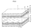
- Figs. 1 and 2 are diagrams showing liquid crystal display devices prepared in the examples of the present invention.
- Figs. 3 and 4 are diagrams showing a preparing process of non-translucent low resistive conductive film for the liquid crystal display device of the present invention.
- Fig. 6 is an explanatory view of function of conventional ferroelectric liquid crystals.
- Fig. 7 is a diagram showing a conventional liquid crystal display device.
- Fig. 8 is a diagram showing pixel part and non-pixel part in their displaying state.
- a number of parallel linear transparent electrodes are formed on the translucent substrates.
- the translucent substrates may be made of glass or the like.
- the linear transparent electrodes and the corresponding ones on the respective substrates each so arranged as the extending directions of the electrodes being intersected are provided for applying voltage through the intersections to liquid crystals disposed between the substrates.
- a transparent conductive film may be prepared on the translucent substrate and etched in a predetermined pattern to form the linear transparent electrodes.
- the transparent conductive film may be ITO film (Indium Tin Oxide), In2O3, SnO2 or the like in thickness of 0.05 to 0.3 ⁇ m.
- the above pattern is provided by etching the transparent conductive film according to a customary method to form lines of 1 to 500 ⁇ m in width.
- the linear transparent electrodes are preferably many and parallel to each other in intervals of 1 to 100 ⁇ m.
- a longitudinally extending insulating film is formed above the ends of one of the adjacent transparent electrodes defining regions therebetween.
- the insulating film insulates the liner transparent electrodes for preventing short-circuiting between the adjacent linear transparent electrodes due to non-translucent low resistive conductive film which is to be formed on the insulating film.
- the insulating film may be provided on a surface of the translucent substrate forming the linear transparent electrodes and etched in a predetermined pattern.
- the insulating film may use Ta2O5 , Al2O3, ZnO, Y2O3, SiO2 or SiN x formed by sputtering, CVD process or the like, and its thickness is generally in the range from 1000 ⁇ to 10000 ⁇ preferably about 5000 ⁇ from the viewpoint of relevant insulating efficiency.
- the pattern preferably allows the insulating film to extend lengthwise above one end of each linear transparent electrode and comprises layers covering an edge and upper surface of that one end.
- Non-translucent low resistive conductive film which shields regions between the adjacent linear transparent electrodes, keeping insulation between the electrodes through an insulating film while it is electrically connected with one of the pair of adjacent transparent electrodes.
- the non-translucent low resistive conductive film applies voltage to the linear transparent electrodes without occurrence of voltage drop in the longitudinal direction of the electrodes, and makes non-translucent the regions defined between the linear transparent electrodes.
- the conductive film preferably has non-translucency and resistivity less than 107 ⁇ cm and may be formed by that molybdenum, aluminum or titan is deposited according to sputtering, vacuum deposition or the like on the insulating film formed on the surface of transparent substrate and etched in a predetermined pattern. Thickness of the conductive film is 100 to 10000 ⁇ , preferably 1000 to 2000 ⁇ .
- the above pattern allows the respective regions between the linear transparent electrodes to be electrically connected with one of the adjacent transparent electrodes defining the specific regions but is disconnected from the other adjacent electrode while kept insulated through an insulating film so as to be non-translucent substantially.
- At least one of substrates provided with a number of parallel linear transparent electrodes and an orientation film formed thereon through an insulating film as or when required may use the above substrate for liquid crystals, and the substrates are arranged as opposing to each other, allowing the extending directions of the linear transparent electrodes to intersect and placing a liquid crystal composition between the substrates, thereby constituting a liquid crystal display device.
- the non-translucent low resistive conductive film is adapted to be electrically connected with one of the adjacent linear transparent electrodes defining the specific regions and be disconnected from the other adjacent electrode through an insulating film by the conductive film's complete shielding of non-pixel part. Hence, the other parts than the pixel regions are shielded from light, thereby unifying the quality of displayed image. Also, decay of voltage to be applied to the electrodes can be lowered to unify voltage to be applied to the liquid crystal layer.
- Fig. 1 shows a ferroelectric liquid crystal display device prepared by the example of the present invention.
- the ferroelectric liquid crystal display device 1 comprises a transparent substrate 2, 3 of glass which seal ferroelectric liquid crystals 4 therebetween.
- Linear transparent electrodes 5 and 6 are formed as stripes constituting a matrix structure on the opposite surfaces of the substrates 2 and 3.
- Non-translucent low resistive conductive films (molybdenum films) 9, 10 are provided as connected with one of the adjacent linear transparent electrodes but disconnected from the other adjacent electrode to provide a complete shading between the adjacent electrodes through an insulating film 7, 8.
- an insulating film 11, 12 and an orientation film 13, 14 are layered in this order on the conductive films.
- Polarizing plates 15, 16 are disposed forming crossed-Nicols on the outer surfaces of the transparent substrates 2 and 3.
- Ta2O5 is deposited on the substrates 2 and 3 to form the insulating films 7, 8 and molybdenum to form the non-translucent low resistive conductive films 9, 10 according to sputtering process, and etched into a shape as shown.
- Fig. 3 shows a process for preparing the insulating films 7,8 and non-translucent low resistive conductive films 9, 10 on the transparent substrates 2, 3.
- Photoresist 37 is then coated thereon, as shown in Fig. 3(b), and baked at 90°C followed by application of light with high pressure mercury lamp through a photo-mask 38 in the shown shape and development of the pattern. Then, the product is baked again at 120°C to form a photoresist pattern 37′ as shown in Fig.
- Molybdenum film 9 as shown in Fig. 3(e) is formed according to sputtering process and subjected to the same process as Figs. 3(b) and (c) using a photomask in the shown shape to form a photo resist pattern 37a′ as shown in Fig. 3(f).
- the product is etched for 3 min by use of a solution containing 25% of 5:1 mixture of H3PO4 and HNO3 to peel off the molybdenum low resistive conductive film 9 except its portion which contacts with one the adjacent linear transparent electrodes and completely shuts light between the specific electrodes followed by peeling off the resist by use of a solution containing 2% of NaOH, as shown in Fig. 3(g).
- the pattern is then spin-coated with SiO2 (Tradename OCD TYPE-II, Tokyo Oka Inc.) and baked to form an insulating film 11 on which a solution of nylon 6 (Toray Industries) in 1% m-cresol was spin-coated followed by baking to form an orientation film 13.
- SiO2 Tradename OCD TYPE-II, Tokyo Oka Inc.
- nylon 6 Toray Industries
- the resultant orientation film 13 on the transparent substrate 2 and the orientation film 14 on the substrate 3 treated similarly with Fig. 3 process are rubbed to be parallel or anti-parallel and configurated into a cell in thickness of 2.0 ⁇ m in which ferroelectric liquid crystals are fed and sealed.
- Two polarizing plates 15 and 16 are disposed on the outer surface of the cell to form a liquid crystal display device shown in Fig. 1.
- the liquid crystal display device comprises molybdenum film which has lower electrical resistivity than the linear transparent electrodes 2 and 3 and extends lengthwise thereof. Hence, voltage to be applied from one end of the electrodes 2, 3 does not decay at the other ends thereof, thereby achieving an excellent bistable memory at the pixel part of matrix electrodes over the whole screen and providing a uniform quality of displayed image at non-pixel part because of a complete cutting off of light by the molybdenum film.
- Al2O3, ZnO, Y2O3, SiO2, SiN x in place of Ta2O5 were used as an insulating film to provide the same effect.
- aluminum, titan or the like in place of molybdenum was used as non-translucent low resistive conductive film to provide the same effect.
- An insulating film to be formed between the linear transparent electrodes and the non-translucent low resistive conductive film is 1000 ⁇ - 10000 ⁇ preferably about 5000 ⁇ in thickness to prevent the electrodes from contacting with the conductive film.
- Fig. 2 shows a ferroelectric liquid crystal display device prepared by the example of the present invention.
- the ferroelectric liquid crystal display device 1 comprises a transparent substrate 2, 3 of glass which seal ferroelectric liquid crystals 4 therebetween.
- Linear transparent electrodes 5 and 6 are formed as stripes constituting a matrix structure on the opposite surfaces of the substrates 2 and 3.
- Non-translucent low resistive conductive films (molybdenum films) 9, 10 are provided as connected with one of the adjacent linear transparent electrodes but disconnected from the other adjacent electrode to provide a complete shading between the adjacent electrodes through an insulating film 7, 8.
- an insulating film 11, 12 and an orientation film 13, 14 are layered in this order on the conductive films.
- Polarizing plates 15, 16 are disposed forming crossed-Nicols on the outer surfaces of the transparent substrates 2 and 3.
- Fig. 4 shows a process for preparing the insulating films 7,8 and non-translucent low resistive conductive films 9, 10 on the transparent substrates 2, 3.
- the drawings show only the case of transparent substrate 2.
- Photoresist 37 is then coated thereon, as shown in Fig. 4(b), and baked at 90°C followed by application of light with high pressure mercury lamp through a photo-mask 40 in the shown shape and development of the pattern. Then, the product is baked again at 120°C to form a photoresist pattern 37′ as shown in Fig.
- Molybdenum film 9 as shown in Fig. 4(e) is formed according to sputtering process and subjected to the same process as Figs. 4(b) and (c) using a photomask 39 in the shown shape to form a photo resist pattern 37a′ as shown in Fig. 4(f).
- the product is etched for 3 min by use of a solution containing 25% of 5:1 mixture of H3PO4 and HNO3 to peel off the molybdenum low resistive conductive film 9 except its portion which contacts with one the adjacent linear transparent electrodes and completely shuts light between the specific electrodes followed by peeling off the resist by use of a solution containing 2% of NaOH, as shown in Fig. 4(g).
- the pattern is then spin-coated with SiO2 (Tradename OCD TYPE-II, Tokyo Oka Inc.) and baked to form an insulating film 11 on which a solution of nylon 6 (Toray Industries) in 1% m-cresol was spin-coated followed by baking to form an orientation film 13.
- SiO2 Tradename OCD TYPE-II, Tokyo Oka Inc.
- nylon 6 Toray Industries
- the resultant orientation film 13 on the transparent substrate 2 and the orientation film 14 on the substrate 3 treated similarly with Fig. 3 process are rubbed to be parallel or anti-parallel and configurated into a cell in thickness of 2.0 ⁇ m in which ferroelectric liquid crystals are fed and sealed.
- Two polarizing plates 15 and 16 are disposed on the outer surface of the cell to form a liquid crystal display device shown in Fig. 2.
- the liquid crystal display device comprises molybdenum film which has lower electrical resistivity than the linear transparent electrodes 2 and 3 and extends lengthwise thereof. Hence, voltage to be applied from one end of the electrodes 2, 3 does not decay at the other ends thereof, thereby achieving an excellent bistable memory at the pixel part of matrix electrodes over the whole screen and providing a uniform quality of displayed image at non-pixel part because of a complete cutting off of light by the molybdenum film.
- Al2O3, ZnO, Y2O3, SiO2 , SiN x in place of Ta2O5 were used as an insulating film to provide the same effect.
- aluminum, titan or the like in place of molybdenum was used as non-translucent low resistive conductive film to provide the same effect.
- An insulating film to be formed between the linear transparent electrodes and the non-translucent low resistive conductive film is preferably more than 1000 ⁇ in thickness to prevent contact the electrodes and the conductive film.
- voltage to be applied to the linear transparent electrodes does not decay. Also, by completely cutting off light at non-pixel part a uniform and bistable memory effect can be obtained at pixel part in the whole screen, and there causes no mixture of bright and dark regions at non-pixel part to thereby provide a uniform bright and dark displaying.
Landscapes
- Physics & Mathematics (AREA)
- Nonlinear Science (AREA)
- Mathematical Physics (AREA)
- Chemical & Material Sciences (AREA)
- Crystallography & Structural Chemistry (AREA)
- General Physics & Mathematics (AREA)
- Optics & Photonics (AREA)
- Geometry (AREA)
- Liquid Crystal (AREA)
Applications Claiming Priority (2)
| Application Number | Priority Date | Filing Date | Title |
|---|---|---|---|
| JP237451/90 | 1990-09-07 | ||
| JP2237451A JPH04116620A (ja) | 1990-09-07 | 1990-09-07 | 液晶表示装置 |
Publications (3)
| Publication Number | Publication Date |
|---|---|
| EP0474507A2 true EP0474507A2 (fr) | 1992-03-11 |
| EP0474507A3 EP0474507A3 (en) | 1992-09-02 |
| EP0474507B1 EP0474507B1 (fr) | 1996-02-28 |
Family
ID=17015540
Family Applications (1)
| Application Number | Title | Priority Date | Filing Date |
|---|---|---|---|
| EP91308173A Expired - Lifetime EP0474507B1 (fr) | 1990-09-07 | 1991-09-06 | Dispositif d'affichage à cristal liquide |
Country Status (5)
| Country | Link |
|---|---|
| US (1) | US5227899A (fr) |
| EP (1) | EP0474507B1 (fr) |
| JP (1) | JPH04116620A (fr) |
| KR (1) | KR920006787A (fr) |
| DE (1) | DE69117398T2 (fr) |
Cited By (1)
| Publication number | Priority date | Publication date | Assignee | Title |
|---|---|---|---|---|
| WO1995002846A1 (fr) * | 1993-07-17 | 1995-01-26 | Central Research Laboratories Limited | Modulateur de lumiere |
Families Citing this family (9)
| Publication number | Priority date | Publication date | Assignee | Title |
|---|---|---|---|---|
| JPH0690375B2 (ja) * | 1986-04-17 | 1994-11-14 | キヤノン株式会社 | 液晶装置 |
| JP2673460B2 (ja) * | 1990-02-26 | 1997-11-05 | キヤノン株式会社 | 液晶表示素子 |
| JP3119935B2 (ja) * | 1992-04-28 | 2000-12-25 | 株式会社半導体エネルギー研究所 | 表示装置の駆動方法 |
| US5622163A (en) | 1994-11-29 | 1997-04-22 | Iep Group, Inc. | Counter for fluid dispensers |
| US5777710A (en) * | 1995-04-28 | 1998-07-07 | Canon Kabushiki Kaisha | Electrode substrate, making the same, liquid crystal device provided therewith, and making the same |
| DE19631922C2 (de) * | 1995-08-07 | 2003-12-04 | Mitsubishi Motors Corp | Abgasmeßvorrichtung |
| US5805254A (en) * | 1995-10-12 | 1998-09-08 | Canon Kabushiki Kaisha | Liquid crystal device and process for production thereof having plural insulating layers |
| US6204902B1 (en) * | 1998-01-14 | 2001-03-20 | Samsung Display Devices Co., Ltd. | Flexible plate liquid crystal display device |
| JP3617458B2 (ja) * | 2000-02-18 | 2005-02-02 | セイコーエプソン株式会社 | 表示装置用基板、液晶装置及び電子機器 |
Family Cites Families (7)
| Publication number | Priority date | Publication date | Assignee | Title |
|---|---|---|---|---|
| JPS6146931A (ja) * | 1984-08-11 | 1986-03-07 | Citizen Watch Co Ltd | カラ−液晶パネルの製造方法 |
| JPS62119521A (ja) * | 1985-11-19 | 1987-05-30 | Canon Inc | 光学変調装置 |
| JPH0666016B2 (ja) * | 1987-05-28 | 1994-08-24 | キヤノン株式会社 | 液晶素子 |
| US5000545A (en) * | 1987-05-28 | 1991-03-19 | Canon Kabushiki Kaisha | Liquid crystal device with metal electrode partially overlying transparent electrode |
| JP2683032B2 (ja) * | 1988-05-06 | 1997-11-26 | キヤノン株式会社 | 液晶素子 |
| JPH01179915A (ja) * | 1988-01-11 | 1989-07-18 | Canon Inc | 液晶素子 |
| JP2670450B2 (ja) * | 1988-08-30 | 1997-10-29 | キヤノン株式会社 | 光学変調素子 |
-
1990
- 1990-09-07 JP JP2237451A patent/JPH04116620A/ja active Pending
-
1991
- 1991-09-03 KR KR1019910015344A patent/KR920006787A/ko not_active Ceased
- 1991-09-05 US US07/755,109 patent/US5227899A/en not_active Expired - Lifetime
- 1991-09-06 EP EP91308173A patent/EP0474507B1/fr not_active Expired - Lifetime
- 1991-09-06 DE DE69117398T patent/DE69117398T2/de not_active Expired - Fee Related
Cited By (1)
| Publication number | Priority date | Publication date | Assignee | Title |
|---|---|---|---|---|
| WO1995002846A1 (fr) * | 1993-07-17 | 1995-01-26 | Central Research Laboratories Limited | Modulateur de lumiere |
Also Published As
| Publication number | Publication date |
|---|---|
| DE69117398T2 (de) | 1996-08-01 |
| KR920006787A (ko) | 1992-04-28 |
| JPH04116620A (ja) | 1992-04-17 |
| EP0474507B1 (fr) | 1996-02-28 |
| EP0474507A3 (en) | 1992-09-02 |
| DE69117398D1 (de) | 1996-04-04 |
| US5227899A (en) | 1993-07-13 |
Similar Documents
| Publication | Publication Date | Title |
|---|---|---|
| EP0534467B1 (fr) | Structure d'électrodes d'un dispositif d'affichage à cristal liquide et procédé de fabrication de dispositif d'affichage à cristal liquide | |
| KR100276442B1 (ko) | 액정표시장치 제조방법 및 그 제조방법에 의한 액정표시장치 | |
| US5633738A (en) | TFT substrate having scanning lines of metal films of columnar crystal grains | |
| US5161043A (en) | Method of forming liquid crystal display device with molybdenum shading layer over ITO electrodes | |
| EP0845696B1 (fr) | Elément d'affichage à cristaux liquides | |
| US20010052951A1 (en) | Liquid crystal display device | |
| EP0512840A2 (fr) | Dispositif d'affichage à matrice active | |
| EP0474507B1 (fr) | Dispositif d'affichage à cristal liquide | |
| KR100482167B1 (ko) | 액정표시장치및그제조방법 | |
| JPH06235940A (ja) | 反射型液晶表示装置 | |
| JP2622033B2 (ja) | 液晶表示装置 | |
| EP0475747A2 (fr) | Dispositif d'affichage à cristal liquide | |
| EP0407164B1 (fr) | Dispositif d'affichage à cristal liquide | |
| JPH06160877A (ja) | 薄膜配線構造及びそれを用いた液晶表示装置 | |
| JP2756147B2 (ja) | 液晶表示装置 | |
| JPH06208114A (ja) | 低抵抗電極を用いた液晶表示素子 | |
| WO2005040905A1 (fr) | Panneau de diodes a couches minces et procede permettant de produire ce panneau | |
| US5231526A (en) | Liquid crystal display device with two insulating films, the second in only non-pixel areas | |
| JPH05142578A (ja) | 液晶表示装置 | |
| JP2654661B2 (ja) | 電気光学表示装置 | |
| JP3350486B2 (ja) | アクティブマトリクス型液晶表示装置 | |
| JP2520604B2 (ja) | 液晶素子及びその製造方法 | |
| JP3657713B2 (ja) | 液晶表示装置 | |
| JPH0262518A (ja) | 液晶画像表示装置 | |
| JPH0593912A (ja) | 液晶表示装置 |
Legal Events
| Date | Code | Title | Description |
|---|---|---|---|
| PUAI | Public reference made under article 153(3) epc to a published international application that has entered the european phase |
Free format text: ORIGINAL CODE: 0009012 |
|
| AK | Designated contracting states |
Kind code of ref document: A2 Designated state(s): DE GB NL |
|
| PUAL | Search report despatched |
Free format text: ORIGINAL CODE: 0009013 |
|
| AK | Designated contracting states |
Kind code of ref document: A3 Designated state(s): DE GB NL |
|
| 17P | Request for examination filed |
Effective date: 19930301 |
|
| 17Q | First examination report despatched |
Effective date: 19941031 |
|
| GRAA | (expected) grant |
Free format text: ORIGINAL CODE: 0009210 |
|
| AK | Designated contracting states |
Kind code of ref document: B1 Designated state(s): DE GB NL |
|
| REF | Corresponds to: |
Ref document number: 69117398 Country of ref document: DE Date of ref document: 19960404 |
|
| PLBE | No opposition filed within time limit |
Free format text: ORIGINAL CODE: 0009261 |
|
| STAA | Information on the status of an ep patent application or granted ep patent |
Free format text: STATUS: NO OPPOSITION FILED WITHIN TIME LIMIT |
|
| 26N | No opposition filed | ||
| PGFP | Annual fee paid to national office [announced via postgrant information from national office to epo] |
Ref country code: DE Payment date: 20010828 Year of fee payment: 11 |
|
| PGFP | Annual fee paid to national office [announced via postgrant information from national office to epo] |
Ref country code: GB Payment date: 20010905 Year of fee payment: 11 |
|
| PGFP | Annual fee paid to national office [announced via postgrant information from national office to epo] |
Ref country code: NL Payment date: 20010927 Year of fee payment: 11 |
|
| REG | Reference to a national code |
Ref country code: GB Ref legal event code: IF02 |
|
| PG25 | Lapsed in a contracting state [announced via postgrant information from national office to epo] |
Ref country code: GB Free format text: LAPSE BECAUSE OF NON-PAYMENT OF DUE FEES Effective date: 20020906 |
|
| PG25 | Lapsed in a contracting state [announced via postgrant information from national office to epo] |
Ref country code: NL Free format text: LAPSE BECAUSE OF NON-PAYMENT OF DUE FEES Effective date: 20030401 Ref country code: DE Free format text: LAPSE BECAUSE OF NON-PAYMENT OF DUE FEES Effective date: 20030401 |
|
| GBPC | Gb: european patent ceased through non-payment of renewal fee |
Effective date: 20020906 |