EP0471130B1 - Kodierungsverfahren und Vorrichtung zur Pipeline- und Parallelverarbeitung - Google Patents
Kodierungsverfahren und Vorrichtung zur Pipeline- und Parallelverarbeitung Download PDFInfo
- Publication number
- EP0471130B1 EP0471130B1 EP90810614A EP90810614A EP0471130B1 EP 0471130 B1 EP0471130 B1 EP 0471130B1 EP 90810614 A EP90810614 A EP 90810614A EP 90810614 A EP90810614 A EP 90810614A EP 0471130 B1 EP0471130 B1 EP 0471130B1
- Authority
- EP
- European Patent Office
- Prior art keywords
- bit
- coder
- byte
- state
- bytes
- Prior art date
- Legal status (The legal status is an assumption and is not a legal conclusion. Google has not performed a legal analysis and makes no representation as to the accuracy of the status listed.)
- Expired - Lifetime
Links
- 238000000034 method Methods 0.000 title claims description 25
- 238000012545 processing Methods 0.000 title description 3
- 230000007704 transition Effects 0.000 claims description 68
- 238000006243 chemical reaction Methods 0.000 claims description 6
- 230000000295 complement effect Effects 0.000 claims description 6
- 230000005540 biological transmission Effects 0.000 description 14
- 238000010586 diagram Methods 0.000 description 9
- 238000001228 spectrum Methods 0.000 description 4
- 238000013461 design Methods 0.000 description 3
- 230000008901 benefit Effects 0.000 description 2
- 230000008859 change Effects 0.000 description 2
- 238000010168 coupling process Methods 0.000 description 2
- 238000005859 coupling reaction Methods 0.000 description 2
- 230000007423 decrease Effects 0.000 description 2
- 238000001514 detection method Methods 0.000 description 2
- 238000009432 framing Methods 0.000 description 2
- 238000013507 mapping Methods 0.000 description 2
- 230000003287 optical effect Effects 0.000 description 2
- 238000011084 recovery Methods 0.000 description 2
- 238000012546 transfer Methods 0.000 description 2
- 230000015556 catabolic process Effects 0.000 description 1
- 238000010276 construction Methods 0.000 description 1
- 230000006735 deficit Effects 0.000 description 1
- 238000006731 degradation reaction Methods 0.000 description 1
- 230000001934 delay Effects 0.000 description 1
- 230000001419 dependent effect Effects 0.000 description 1
- 238000003780 insertion Methods 0.000 description 1
- 230000037431 insertion Effects 0.000 description 1
- 239000000203 mixture Substances 0.000 description 1
- 239000013307 optical fiber Substances 0.000 description 1
- 230000003071 parasitic effect Effects 0.000 description 1
- 230000008569 process Effects 0.000 description 1
- 230000001902 propagating effect Effects 0.000 description 1
- 230000009467 reduction Effects 0.000 description 1
- 230000003595 spectral effect Effects 0.000 description 1
- 230000001629 suppression Effects 0.000 description 1
Images


Classifications
-
- H—ELECTRICITY
- H03—ELECTRONIC CIRCUITRY
- H03M—CODING; DECODING; CODE CONVERSION IN GENERAL
- H03M5/00—Conversion of the form of the representation of individual digits
- H03M5/02—Conversion to or from representation by pulses
- H03M5/04—Conversion to or from representation by pulses the pulses having two levels
- H03M5/14—Code representation, e.g. transition, for a given bit cell depending on the information in one or more adjacent bit cells, e.g. delay modulation code, double density code
- H03M5/145—Conversion to or from block codes or representations thereof
-
- G—PHYSICS
- G11—INFORMATION STORAGE
- G11B—INFORMATION STORAGE BASED ON RELATIVE MOVEMENT BETWEEN RECORD CARRIER AND TRANSDUCER
- G11B20/00—Signal processing not specific to the method of recording or reproducing; Circuits therefor
- G11B20/10—Digital recording or reproducing
- G11B20/14—Digital recording or reproducing using self-clocking codes
- G11B20/1403—Digital recording or reproducing using self-clocking codes characterised by the use of two levels
- G11B20/1423—Code representation depending on subsequent bits, e.g. delay modulation, double density code, Miller code
- G11B20/1426—Code representation depending on subsequent bits, e.g. delay modulation, double density code, Miller code conversion to or from block codes or representations thereof
-
- H—ELECTRICITY
- H04—ELECTRIC COMMUNICATION TECHNIQUE
- H04L—TRANSMISSION OF DIGITAL INFORMATION, e.g. TELEGRAPHIC COMMUNICATION
- H04L25/00—Baseband systems
- H04L25/38—Synchronous or start-stop systems, e.g. for Baudot code
- H04L25/40—Transmitting circuits; Receiving circuits
- H04L25/49—Transmitting circuits; Receiving circuits using code conversion at the transmitter; using predistortion; using insertion of idle bits for obtaining a desired frequency spectrum; using three or more amplitude levels ; Baseband coding techniques specific to data transmission systems
- H04L25/4906—Transmitting circuits; Receiving circuits using code conversion at the transmitter; using predistortion; using insertion of idle bits for obtaining a desired frequency spectrum; using three or more amplitude levels ; Baseband coding techniques specific to data transmission systems using binary codes
- H04L25/4908—Transmitting circuits; Receiving circuits using code conversion at the transmitter; using predistortion; using insertion of idle bits for obtaining a desired frequency spectrum; using three or more amplitude levels ; Baseband coding techniques specific to data transmission systems using binary codes using mBnB codes
-
- G—PHYSICS
- G11—INFORMATION STORAGE
- G11B—INFORMATION STORAGE BASED ON RELATIVE MOVEMENT BETWEEN RECORD CARRIER AND TRANSDUCER
- G11B20/00—Signal processing not specific to the method of recording or reproducing; Circuits therefor
- G11B20/10—Digital recording or reproducing
- G11B20/14—Digital recording or reproducing using self-clocking codes
- G11B20/1403—Digital recording or reproducing using self-clocking codes characterised by the use of two levels
- G11B20/1423—Code representation depending on subsequent bits, e.g. delay modulation, double density code, Miller code
- G11B20/1426—Code representation depending on subsequent bits, e.g. delay modulation, double density code, Miller code conversion to or from block codes or representations thereof
- G11B2020/1438—8 to 10 modulation
Definitions
- Present invention is concerned with the encoding of sequential data bytes each comprising k bits, into code bytes each comprising m bits, i.e. kB/mB coding with k ⁇ m, where the sequential data bytes have no restrictions, but any sequence of code bytes is constrained (e.g. bounded running digital sum RDS; limited run-length of identical symbols).
- the present invention is concerned with a coder in which a group of several sequential data bytes can be converted simultaneously into a respective group of code bytes.
- the coding technique of present invention may find application in digital data transmission as well as in magnetic or optical recording of digital data.
- Line codes impose desired constraints on transmitted signals to facilitate detection in the presence of the usual transmission impairments.
- Signal characteristics required often in practice are spectral null at DC, spectrum with small low-frequency content, small maximum distance between transitions from one signal level to another one, and large minimum and average transition density.
- binary transmission or recording schemes such as the ones used in fiber-optical transmission and in digital magnetic recording, these desired properties of the transmitted signal can only be achieved by an increase in the channel data rate, i.e., insertion of redundancy into the data stream (coding without enlarging the set of signal levels).
- kB/mB block codes where a k-bit byte of data is mapped into an m-bit code byte are very common. Coding schemes considered here in particular are 8B/10B block codes.
- the desired properties of a line code are determined by the field of application.
- DC-free transmission codes are preferred because laser diode transmitters and high-sensitivity receivers are usually AC-coupled designs specified by a lower and an upper frequency limit for operation.
- the upper frequency limit indicates the maximum achievable channel data rate whereas the lower frequency limit determines the amount of tolerable low-frequency content in the signal spectrum.
- the lower frequency limit in the laser diode driver is determined by the control loop which keeps the average output power at a constant level.
- DC-free transmitted signals do not require a data-reference circuit in the transmitter which have been used to cope with DC-shifted signals.
- the lower frequency limit in the receiver is given by the AC-coupling of the analog preamplifier stages which allows better control of parasitic noise in the design of high-performance amplifier front-end circuits.
- a code is DC-free if and only if the running digital sum (RDS) is bounded.
- the number of values RDS can take on determines the low-frequency content of the code spectrum and will be denoted by V.
- the digital sum variation (DSV) is then given by V-1. Capacity calculations show that V cannot be made smaller than six for a code rate 8/10. It is also true that the smaller V (or DSV) the larger the suppression of the power at low-frequencies in the code spectrum to facilitate AC-coupling.
- the decoders for line codes are usually block decoders to avoid infinite error propagation.
- a block decoder for a kB/mB code has the desirable property that errors in a single m-bit code byte at its input can only affect a single k-bit data byte at its output.
- Such a block decoder can also be used to detect invalid code bytes by raising a flag if the input of the decoder is a m-bit byte which is not a permitted code byte.
- Another important aspect of a block decoder is its synchronization, i.e., the capability to infer from the incoming serial stream of bits where the code byte boundaries are.
- the j-bit sync pattern is chosen such that it cannot occur anywhere in the stream of code bytes.
- Another desired property associated with a sync byte is that it differs from all code bytes in two or more bits to decrease the probability of a code byte being mistaken for a sync byte because of transmission errors.
- kB/mB line code provides an adequate number of special m-bit bytes which can be used for framing and control purposes. These special bytes, which do not represent data, should satisfy the code constraints. Finally, encoders/decoders at very high channel data rates should offer multiple-byte interface for implementation and interconnection reasons.
- a DC-free partitioned block 8B/10B code for packet transmission on optical fibers was described in U.S.Patent 4,486,739 (Widmer and Franaszek).
- One of the sync bytes differs from all code bytes in two or more bits. However, the repetition of this particular sync byte is not permitted.
- the other two sync bytes differ from some code bytes in only one bit and can be repeated with a transition density of 30% and 50%.
- the logic gates used for implementing the code are required to have gate delays of no more than a baud interval. Considering that a channel data rate of 2.4 Gbit/s corresponds to a gate delay of 0.416 ns, the implementation of this coding scheme at this speed becomes very difficult.
- U.S.Patent 4,488,142 (Franaszek) and U.S.Patent 4,888,779 (Karabed and Siegel) both disclose coding apparatus in which the coder receives, besides a next group of input data bits, coder state information which is derived from the encoded data.
- coder state information which is derived from the encoded data.
- no parallel encoding is possible with these coders because the coder state information is obtained only at the output of the encoder apparatus.
- DE-Al-3 608 357 discloses a kB/mB coding method with four parallel converting sections. However, no state machine is employed.
- the encoder apparatus has the great advantage that due to parallel and pipelined encoding, very high speed operation can be achieved which is necessary e.g. when data are to be transmitted at Gbit/s rates over optical links.
- the proposed transmission code is DC-free and allows an AC-coupled implementation leading to a substantial reduction in circuit count by avoiding the use of bias-restoration circuits.
- Table 1 and Table 2 present a selection of 10-bit code bytes to be used as ROM contents in the encoder apparatus of Fig.6A/6B, providing the required code constraints.
- bit is used to designate any bit group comprising a predetermined number of bits, e.g. 8-bit data bytes and 10-bit code bytes, or generally k-bit data bytes and m-bit code bytes. A given number of bytes may form a word, e.g. four 10-bit code bytes may constitute a 40-bit code word.
- byte in the following description is not restricted to 8-bit entities.
- data word and "code word” are used for those bit groups which are designated as bytes in the present description.
- Essential features of the invented method and apparatus are a state transition function T and a coder state function S. While in a general case they will be multiple valued functions termed “state transition indicator T” and “coder state indicator S”, these functions are binary in the disclosed preferred embodiment of a two-state coder, and therefore are termed in the description "state transition bit T” and "coder state bit S”.
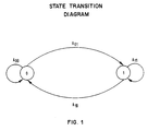
- FIG.1 A state transition diagram illustrating the two coder states and the four coder state transitions which are provided in the preferred embodiment of the invented coding scheme is shown in Fig.1.
- a conversion is made from k-bit data bytes to m-bit code bytes.
- 128
- the coder state at time n is equal to the running digital sum (RDS) achieved after generating a code byte at time n-1.
- the code bytes in A00 and A11 have disparity 0 (they have five 0's and five 1's) whereas the code bytes in A01 and A10 have disparity +2 (they have four 0's and six 1's) and -2 (they have six 0's and four 1's), respectively.
- the code bytes in A00, A01, A10 and A11 are chosen such that they satisfy the following four constraints:
- None of the code bytes in A00, A01, A10 and A11 does contain six (or more) consecutive 0's or 1's.
- the code bytes A00 and A10 leading to state 0 do not end with four 0's or three 1's, and the code bytes A01 and A11 leading to state 1 do not end with four 1's or three 0's; furthermore, the code bytes in A00 and A01 emanating from state 0 do not begin with four 1's or three 0's, and the code bytes in A10 and A11 emanating from state 1 do not begin with four 0's or three 1's.
- a minimum transition density of TD min 40% is ensured by choosing all the code bytes such that they have at least four transitions where a transition occurs if a zero follows a one or a one follows a zero.
- the code bytes a1 a2 ... a10 in A00 or A01 must be chosen such that -3 ⁇ -1 + b1 + b2 + ⁇ + b i ⁇ +3 and the code bytes a1 a2 ...
- Frame synchronization is achieved by sending sync bytes prior to the transmission of data.
- the sync byte generated when the encoder is in state 0 (1) is chosen to be 0101111100 (1010000011) and imbeds the unique sync pattern 1011111 (0100000).
- a stream of sync bytes then has a transition density of 50%.
- the code bytes are chosen such that both sync patterns cannot occur anywhere in a stream of code bytes in order to enable the decoder to realign the code byte boundaries after loss of synchronization. All the code bytes which differ from a sync byte or its complement in only one bit are also not allowed to occur. This decreases the likelihood of a code byte being mistaken for a sync byte because of transmission errors and vice versa. It should be noted that during transmission of the synchronization sequence consisting of sequential sync bytes, the coder state changes after each sync byte, i.e. the two complementary sync bytes are used alternatingly.
- Tables 1 and 2 give two lists P and Q of potential code bytes containing 161 and 129 ten-bit bytes, respectively.
- the two lists P and Q were obtained following the rules given above.
- the concatenation of bytes in P, Q, P and Q following the state transition rules results in a stream of bytes satisfying the desired constraints.
- Rule 1 ensures that the decoder can be realized as a block decoder mapping the code bytes at its input into the original data bytes. Errors in a ten-bit byte at the input of the block decoder cause only a single decoded data byte being in error. If the decoder input is a ten-bit byte which is not in A00, A01, A10 and A11 the decoder raises a flag indicating the detection of an invalid code byte.
- the 8B/10B block coder/decoder operates in parallel on 2 or 4 bytes. Multiple sets of independent block coders to match the interface data path width are not preferred, because the performance of the code diminishes mainly due to an increase in DSV.
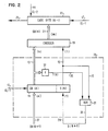
- FIGs.2, 3, and 4 show different forms of a basic coder unit operating according to the invention.
- This unit receives at its input a data byte, and furnishes at its output an encoded byte (or "code byte" as it will be designated shortly in the sequel).
- a register 11 holds the k-bit data byte DB(N) presently being encoded, plus a coder state bit S(N) indicating the encoder state when the respective data byte is encoded.
- the contents of the register had been loaded by a clock signal CL-1 on line 17.
- the data byte is available on lines 13 (k parallel bit lines), the state bit on line 15. Together, they are furnished to encoder 19 which is merely a look-up table furnishing, when addressed by the input on lines 13 and 15, at its output lines 21 an m-bit code byte CB(N). This is stored in an output register 23 under control of the next pulse of clock signal CL-1 on line 17.
- the code byte can be obtained (serially) on an output line 25 when a shift clock signal CL-2 is applied on line 44.
- the next data byte DB(N+1) is presented on input lines 27.
- the next coder state bit S(N+1) will be generated on line 29 in dependence of the old coder state bit S(N) and a function of the old data byte, as was generally explained above:
- the coder state is either changed or not changed, depending on a binary function derived from the old data byte DB(N).
- Logic circuitry 37 is provided for deriving the binary state transition function T (state transition bit T) from the bits of the old data byte DB(N).
- Register 11, XOR gate 31, and logic 37 together form a "data register and coder state block" 39, designated as DRCS block 39 in the sequel, indicated by a dotted line box in Fig.2.
- the basic encoder unit comprises two pipeline stages: Stage 1 consists of the DRCS block 39, preparing the coding of the next data byte DB(N+1); stage 2 is the actual encoder which is merely a table look-up function for converting data byte DB(N) plus its associated state bit S(N) into a code byte CB(N).
- FIG.3 A somewhat simpler form of the basic coder unit is shown in Fig.3.
- the state transition bit T on line 33 is simply identical to the last bit (D7) of the respective data byte. This eliminates the need for logic circuitry 37, as shown in Fig.3.
- this figure shows the preferred data byte length of 8 bits and code byte length of 10 bits.
- the coder is an 8/10 coder.
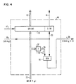
- a modified form of the DRCS block is shown in Fig.4. That modified form of the DRCS block is particularly suited for parallel arrangement of several basic coder units, which is an important advantage of the present invention.
- the modified DRCS block 40 also has a register 11 for holding the data byte DB(N) to be encoded, plus the associated encoder state bit S(N). Both are furnished on output lines 13 and 15, respectively.
- the next data byte DB(N+q) is entered through lines 27. However, the next coder state bit S(N+q) is furnished from another section on line 30.
- a further coder state bit S(N+q+1) is derived in XOR gate 32, by combining coder state bit S(N+q) with a state transition bit T(N+q) on line 34 which in turn is derived by logic 37 from the next data byte DB(N+q) available on lines 27.
- the derived future coder state bit S(N+q+1) is furnished on a line 36. (Of course, a simpler design is also possible for the preferred embodiment, by eliminating logic 37 and just connecting state selection bit line 34 to a single one of the data bit lines 27).
- this encoder principle allows pipelined as well as parallel operation of the encoder.
- Several basic coder units each comprising a modified DRCS block 40 (as shown in Fig.4) and an encoder 19, can be combined in parallel, and the coder state bit can be simultaneously derived for each of them, by propagating it from section to section like a carry function.
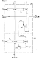
- FIG.5 The block diagram of an encoder comprising four parallel coder sections is shown in Fig.5. It should be noted that it is of course possible to provide a larger number of parallel sections (e.g., 8 or 16) if that is desirable in a system.
- DRCS blocks 40A, 40B, 40C, 40D each accepting on its input lines (27A...27D) one input data byte and providing on its output lines (13A...13D; 15A...15D) a data byte DB to be encoded, and the corresponding coder state bit S.
- each DRCS block one output (36A...36D) furnishing a coder state bit for the next section, is connected to an input (30B, 30C, 30D, 30A) of the DRCS block for the next data byte; in the return connection between the last section D and the first section A, i.e. between output 36D and input 30A, there is provided a clocked delay stage 42 so that the coder state bit generated in the last section is entered into the first section only one clock interval later. This together constitutes the pipeline stage 1 of the four-byte parallel encoder (word encoder).
- encoders 19A, 19B, 19C, 19D lookup tables each for encoding one data byte, and furnishing the code bytes on respective output lines (21A...21D).
- the encoders constitute the pipeline stage 2 of the parallel byte encoder (word encoder).
- the coded bytes are loaded into respective output registers (23A...23D) under control of the clock signal CL-1 on line 17. They can be furnished in serial form on output line 26, under control of a shift clock signal CL-2 on line 44.
- the frequency of this shift clock signal is forty times as much as that of the word clock signal CL-1.
- the DRCS blocks (data register and coder state blocks) hold four data bytes DB(N)...DB(N+3), plus their respective associated coder state bits S(N)...S(N+3). They are available also on output lines 13A...13D and 15A...15D, and they address encoders 19A...19D so that at the encoder outputs 21A...21D, the coded bytes CB(N)...CB(N+3) are available simultaneously.
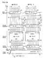
- Figs.6A/6B show a more detailed circuit diagram of a multi-byte block encoder whose principle was shown in Fig.5. Again, the same reference numerals were used for items already shown in Figs.2/3/4 and in Fig.5.
- the encoder comprises four pipeline registers 11A...11D, four encoders (look-up tables) 19A...19D, and four output registers 23A...23D.
- State update is performed by a chain of four XOR gates 32A...32D, and state updating percolates across the 4-byte word thus updating all four coder state bits S.
- a clocked one-bit delay stage 42 is provided for keeping the output of the last XOR gate 32D up to the next clock interval, so that it can then be used for the first pipeline register 11A.
- each data byte DB is designated as D0...D7.
- Fig.6A/6B shows in all data byte registers an additional bit Z, and also an input line Z in parallel with the data bit lines D0...D7.
- These control bits Z are also entered into the pipeline registers, and they are used, together with the associated data byte DB(N) and state bit S(N) as a combined address for accessing the encoder lookup table (19A etc.).
- the respective address bits are designated as A0...A7, A8, and A9 as is shown in Fig.6A/6B.
- Each encoder table is a ROM storing 210 (i.e., 1024) ten-bit code bytes, which is addressed by the 10-bit input present in pipeline register (11A etc.).
- the remaining encoding process effected in pipeline stage 2 is a mere conversion from one set of 10-bit bytes into another.
- each look-up table 19A...19D is a ten-bit code byte Q0...Q9 which is transferred into an output register (23A...23D) (under control of the clock signal CL-1 on line 17).
- the respective decoder for converting a bit stream representing sequential 10-bit code bytes into 8-bit data bytes is shown in Figs.7A/7B.
- Decoding of a byte does not depend at all from previous transmitted bytes and is performed by look-up tables. This feature of the block code prevents any error propagation caused by transmission bit errors. As a consequence, the decoder needs no portions for handling state bits, as is the case for the encoder.
- the coded bit stream appearing on input line 57 is entered into a deserializer 59 under control of a shift clock on line 61.
- the serializer also generates a word clock on line 63 (which furnishes one clock pulse for each group of four bytes, i.e., for each word).
- the decoded data bytes in the present example DB(N-4)...DB(N-1) plus respective control bits Z, are stored in four decoder output registers 69A...69D, under control of the word clock available on line 63. Each byte is then available on respective output lines D0...D7 (71A...71D) and Z (73A...73D).
- a DRCS block data register and coder state block
- a certain transition time is needed after application of a new set of input data bytes, until the state bit S of the last one of the parallel sections assumes its new value.
- This transition time is equal to the transition time of the logic units 37 (changing their states simultaneously in all parallel sections), plus the time needed for the new state values to ripple through the XOR gates 32 of all parallel sections which are arranged in a series connection.
- the maximum rate of the clock signal CL-1 on line 17 depends on the length of this transition time.
- a modified version of the DRCS block can be provided as shown in Fig.8.
- the state transition bit T is derived in advance from the input bytes DB.
- Portion 40-1 of the DRCS block comprises register 11 for the data byte DB(N) presently being encoded and its associated state bit S(N), and an XOR unit 32 for combining the state bit S(N+q) from the neighbor section, and a state transition bit T(N+q) which is provided on line 34′.
- An additional DRCS block portion 40-2 must be provided to allow for the advance generation of the state transition bit T.
- This portion 40-2 comprises an additional register 75 for holding the next data byte DB(N+q) for the respective coder section, plus the respective state transition bit T(N+q).
- the input to register 75 are lines 27′ on which the over-next data byte DB(N+2q) for the respective section is received.
- Logic circuitry 38 is connected to these input lines 27′, for deriving the over-next state transition bit T(N+2q) from the over-next data byte.
- This advance state transition bit will be stored, when the next clock pulse occurs on lines 17, together with the respective data byte in register 75.
- This modified DRCS block allows a faster operation and thus a higher clock rate than the embodiment shown in Fig.4, at the expense of one extra register 75 for each of the parallel byte sections of the encoder.
- the coder state bit S(N+q) for the prestored data byte DB(N+q) is received from the left neighbor section, the necessary state transition bit T(N+q) is stored with the prestored data byte DB(N+q), and in XOR gate 32, the coder state bit S(N+q+1) for the right neighbor section is developed.
- a state transition bit T(N+q-1) and a coder state bit S(N+q-1) could be received from the left neighbor section (which would require two transition lines for T and S instead of only one for S), and the XOR unit would be employed for developing the coder state bit S(N+q), for use in the respective section and for transfer to the right neighbor section.
- the prestored state transition bit T(N+q) then would not be used in the respective section, but would also be transferred to the right neighbor section.
- two delay registers 42 would be required instead of only one.
- byte means any bit group having a predetermined number of bits, as was explained already at the end of the introduction.
- the first and third section could provide p/r block encoding (e.g. 9/10 block encoding), whereas the second and fourth section (which are interconnected with the first and third section) could provide u/w block encoding (e.g. 7/8 block encoding).
- p/r block encoding e.g. 9/10 block encoding
- u/w block encoding e.g. 7/8 block encoding
- coder state function S(i) and the state transition function T(i) have restricted the coder state function S(i) and the state transition function T(i) to binary variables assuming the values 0 or 1. Therefore, they were termed "coder state bit S(i)" and “state transition bit T(i)", respectively, in the description of the preferred embodiment.
- registers should have the appropriate size to be able to store S(i) and T(i).
- register 11 would have to store (k+s) bits whereas register 75 would have to store (k+t) bits.
- the XOR block 31, 32 would have to be replaced by logic circuitry implementing the Boolean function g, and whenever more than one bit is needed to represent S(i) or/and T(i) the corresponding lines would have to be multiple lines for transmitting multi-bit variables.
Landscapes
- Engineering & Computer Science (AREA)
- Signal Processing (AREA)
- Theoretical Computer Science (AREA)
- Physics & Mathematics (AREA)
- Spectroscopy & Molecular Physics (AREA)
- Computer Networks & Wireless Communication (AREA)
- Compression, Expansion, Code Conversion, And Decoders (AREA)
- Dc Digital Transmission (AREA)
Claims (18)
- Verfahren zum Kodieren sequentieller k-Bit Datenbytes in sequentielle m-Bit Kodebytes, die vorbestimmte Begrenzungen erfüllen, wobei k < m, unter Einsatz eines Kodierungsverfahrens mit mindestens zwei Zuständen,
wobei das Verfahren dadurch gekennzeichnet ist, daß es die folgenden Schritte umfaßt:- Erzeugen eines Zustandsübergangsindikators T(i-1) zum Kodieren jedes Datenbytes DB(i), abhängig von den Bitwerten des jeweils vorangehenden Datenbytes DB(i-1); und- paralleles Kodieren von q Datenbytes DB(N)...DB(N + q-1) durch-- gleichzeitiges Erzeugen eines Kodierer-Zustandsindikators S(i) für jedes Datenbyte DB(i) einer Gruppe von q Datenbytes, durch logisches Kombinieren des Kodierer-Zustandsindikators S(i-1), der dem jeweils vorangehenden Datenbyte DB(i-1) zugeordnet ist und des Zustandsübergangsindikators T(i-1), der abhängig von dem jeweils vorangehenden Datenbyte DB(i-1) erzeugt wird, und-- Umwandeln jedes Datenbytes DB(i) der Gruppe von q Datenbytes, zusammen mit dem zugehörigen KodiererZustandsindikator S(i), in ein zugewiesenes m-Bit Kodebyte CB(i). - Ein Verfahren nach Anspruch 1, bei dem- ein Kodierungsverfahren mit zwei Zuständen eingesetzt wird, und- der genannte Kodierer-Zustandsindikator S(i) und der genannte Zustandsübergangsindikator T(i-1) binäre Größen sind, die durch ein Zustandsübergangsbit beziehungsweise ein Kodierer-Zustandsbit dargestellt werden.
- Methode nach Anspruch 2, außerdem weiter folgenden Schritt umfassend:
- logisches Kombinieren des Kodierer-Zustandsbits S(i-1), das dem vorherigen Datenbyte DB(i-1) zugeordnet ist, und des Zustandsübergangsbits T(i-1), das abhängig von dem vorherigen Datenbyte DB(i-1) in einer Exklusiv-Oder-Operation erzeugt wurde, so daß der Wert des Zustandsübergangsbits T(i-1) bestimmt, ob der binäre Kodierer-Zustand, der dem vorherigen Datenbyte zugeordnet ist, für das aktuelle Datenbyte beibehalten oder verändert wird. - Verfahren nach Anspruch 2, folgenden Schritt umfassend:
- Auswählen des Zustandsübergangsbits T(i-1), so daß es einem bestimmten Bit (D7) der Bits des vorherigen Datenbytes DB(i-1) entspricht. - Verfahren nach Anspruch 2, den folgenden weiteren Schritt umfassend:
- Speichern eines Kodierer-Zustandsbits S(N + q), das abhängig von dem letzten Datenbyte DB(N + q-1) der einen Gruppe erzeugt wurde, und seines zugeordneten Kodierer-Zustandsbits S(N + q-1) in einem getrennten Register (42) und Einsetzen dieses Kodierer-Zustandsbits (S(N + q) nach einer vorgegebenen Verzögerung als Eingang zum Kodieren des ersten Datenbytes DB(N + q) der nächsten Gruppe von q Datenbytes DB(N + q) ... DB(N + 2q-1). - Methode nach Anspruch 2, folgende zusätzliche Schritte umfassend:- mit jedem Datenbyte DB(i) Bereitstellen eines zusätzlichen Steuerbits Z(i), um festzustellen, ob das betreffende Datenbyte tatsächliche Daten oder eine Steuerinformation darstellt, und- Umwandeln jedes Datenbytes DB(i) sowie des zugeordneten Kodierer-Zustandsbits S(i) und des zugeordneten Steuerbits Z(i) in ein zugewiesenes Kodebyte CB(i).
- Methode nach Anspruch 1, bei der die m-Bit Kodebytes in jeder möglichen sequentiellen Anordnung die folgenden Begrenzungen erfüllen:- (a) Die Lauflänge identischer Symbole ist auf einen vorbestimmten Wert R begrenzt;- (b) die Übergangsdichte ist nicht geringer, als ein vorbestimmter Wert TDmin;- (c) die laufende digitale Summe RDS kann nur eine vorbestimmte Anzahl V verschiedener Werte annehmen; und- (d) ein vorbestimmtes Synchronisationsmuster SP und sein Komplement
SP kommen nicht vor. - Verfahren nach Anspruch 7, bei dem jedes Kodebyte m = 10 Bits umfaßt, und bei dem die von den Kodebytes erfüllten Begrenzungen die folgenden Werte haben:- (a) die maximale Lauflänge der identische Symbole beträgt R = 5;- (b) die minimale Übergangsdichte beträgt TDmin = 40 %;- (c) die Anzahl der unterschiedlichen Werte für die laufende digitale Summe RDS beträgt V = 7; und- (d) das Synchronisationsmuster SP ist die Bitfolge 1011111, sein Komplement
SP ist die Bitfolge 0100000. - Verfahren nach Anspruch 8, bei dem die Kodebytes zusätzlich folgende Begrenzung erfüllen:
- (e) Ein Synchronisationsbyte, in dem das vorbestimmte Synchronisationsmuster SP (1011111) eingebettet ist, und sein Komplement, in dem das komplementäre SynchronisationsmusterSP (0100000) eingebettet ist, unterscheiden sich von jedem Kodebyte in mindestens zwei Bits. - Kodierervorrichtung zum Kodieren sequentieller k-Bit Datenbytes in sequentielle m-Bit Kodebytes, die vorbestimmte Begrenzungen erfüllen, wobei k < m, in der ein Kodierverfahren mit mindestens zwei Zuständen eingesetzt wird, zum Ausführen des Verfahrens nach Anspruch 1, dadurch gekennzeichnet, daß das Verfahren q parallele Umwandlungsabschnitte, von denen jeder mindestens zwei Pipeline-Stufen aufweist, und einen zugeordneten Kodierer-Zustandsindikator (S(i)) umfaßt,- wobei jeder der genannten parallelen Umwandlungsabschnitte zum Umwandeln eines Eingangsdatenbytes DB(i) in ein Ausgangs-Kodebyte CB(i) vorgesehen ist und folgendes umfaßt:-- in einer ersten Pipeline-Stufe (40) ein Register (11) für ein Datenbyte DB(i) und den zugeordneten Kodierer-Zustandsindikator S(i) und Mittel (32) zum Erzeugen eines neuen Kodierer-Zustandsindikators; und-- in einer zweiten Pipeline-Stufe, Kode-Umwandlungsmittel (19), die als Eingänge (13; 15) ein Datenbyte DB(i) und den zugeordneten Kodierer-Zustandsindikator S(i) empfangen, und die an ihrem Ausgang (21) das entsprechende Kodebyte CB(i) bereitstellen;- Verbindungsmittel (30; 36), die zwischen den ersten Pipeline-Stufen von benachbarten Abschnitten angeordnet sind, zum Übertragen eines Kodierer-Zustandsindikators von einem Abschnitt zum nächsten.
- Kodierervorrichtung nach Anspruch 10, bei der- der neue Kodierer-Zustandsindikator, der in jedem Abschnitt erzeugt wird, der Kodierer-Zustandsindikator S(i + q 1) ist, der dem nächsten Datenbyte DB(i + q + 1), das in dem benachbarten Abschnitt kodiert wird, zugeordnet wird, und- dieser neue Kodierer-Zustandsindikator S(i + q + 1) auf dem genannten Verbindungsmittel (30; 36) zu dem betreffenden Nachbarabschnitt übertragen wird.
- Kodierervorrichtung nach Anspruch 10, bei der- der neue Kodierer-Zustandsindikator, der in jedem Abschnitt erzeugt wird, der Kodierer-Zustandsindikator S(i + q) ist, der dem nächsten Datenbyte DB(i + q) zugeordnet werden muß, das in demselben Abschnitt kodiert werden soll;- dieser neue Kodierer-Zustandsindikator S(i + q) auf dem genannten Verbindungsmittel (30; 36) zu dem betreffenden Nachbarabschnitt übertragen wird;- zusätzliche Zwischenverbindungsmittel bereitgestellt werden, um einen Zustandsübergangsindikator T(i + q) zu dem benachbarten Abschnitt zu übertragen; und- das genannte Mittel (32) zum Erzeugen eines neuen Kodierer-Zustandsindikators als Eingänge einen Kodierer-Zustandsindikator und einen Zustandsübergangsindikator empfängt, die auf dem genannten Zwischenverbindungsmittel und auf dem genannten zusätzlichen Zwischenverbindungsmittel von dem benachbarten Abschnitt übertragen werden.
- Kodierervorrichtung nach Anspruch 10, bei der der genannte Kodierer zwei unterschiedliche Zustände hat, der genannte Zustandsübergangsindikator eine binäre Größe ist, dargestellt durch ein Zustandsübergangsbit T, und der genannte Kodierer-Zustandsindikator eine binäre Größe ist, dargestellt durch ein Kodierer-Zustandsbit S; wobei die genannte Kodierervorrichtung folgendes umfaßt:- Mittel (34, 37; 34′, 38, 75), um ein Zustandsübergangsbit T(N + q) von einem gegebenen Datenbyte DB(N + q) abzuleiten, und- logisches Mittel (32), das das genannte Zustandsübergangsbit T(N + q) und das Kodierer-Zustandsbit S(N + q), die dem genannten gegebenen Datenbyte DB(N + q) zugeordnet sind, kombiniert, und ein neues Kodierer-Zustandsbit S(N + q + 1) bereitstellt, das dem Datenbyte DB(N + q + 1) nach dem genannten gegebenen Datenbyte DB(N + q) zugeordnet wird.
- Kodierervorrichtung nach Anspruch 10, als Kode-Umwandlungsmittel in jedem der q parallelen Abschnitte folgendes umfassend:- Tabellennachschlag-Festspeichermittel (19A...19D), in dem alle möglichen Ausgangs-Kodebytes CB(i) gespeichert werden;- wobei das genannte Tabellennachschlag-Speichermittel von dem Inhalt des genannten Registers (11A...11D) in der ersten Pipeline-Stufe adressiert wird (15A...15D; A0...A9).
- Kodierervorrichtung nach Anspruch 10, weiter umfassend:
- eine zusätzliche dritte Pipeline-Stufe (40-2) in jedem der q parallelen Abschnitte, wobei die genannte dritte Pipeline-Stufe folgendes umfaßt:-- ein zusätzliches Register (75) zum Speichern des Datenbytes DB(N + q) eines nächsten Blocks, das kodiert werden soll, und eines von diesem abgeleiteten Zustandsübergangsindikators T(N + q), und-- logisches Mittel (38), um im voraus einen Zustandsübergangsindikator T(N + 2q) aus einem Vorab-Datenbyte DB(N +2q) des nächsten Blocks zu erzeugen, das am Eingang der genannten dritten Pipeline-Stufe verfügbar ist; wobei der Ausgang des genannten logischen Mittels mit einem Eingang des genannten zusätzlichen Registers (75) verbunden wird. - Kodierervorrichtung nach Anspruch 10, folgendes umfassend:
- mindestens zwei Abschnitte mit unterschiedlichen Registergrößen und einer unterschiedlichen Anzahl von Bitleitungen zum Übertragen von Datenbytes und Kodebytes, um ein gleichzeitiges Kodieren von Datenbytes mit einer ersten Datenbyte-Breite p in Kodebytes mit einer ersten Kodebyte-Breite q in einem Abschnitt zu ermöglichen, und das Kodieren von Datenbytes mit einer zweiten Datenbyte-Breite u in Kodebytes mit einer zweiten Kodebyte-Breite w in einem anderen Abschnitt. - Kodierervorrichtung nach Anspruch 10, in jedem der genannten Register (11A...11D) in der genannten ersten Pipeline-Stufe eine zusätzliche Bitposition für ein Steuerbit Z(i) umfassend; wobei das genannte Kode-Umwandlungsmittel (19) als zusätzlichen Eingang ein Steuerbit Z(i) zusammen mit einem Datenbyte DB(i) und dem zugeordneten Kodierer-Zustandsindikator S(i) empfängt.
Priority Applications (6)
| Application Number | Priority Date | Filing Date | Title |
|---|---|---|---|
| EP90810614A EP0471130B1 (de) | 1990-08-16 | 1990-08-16 | Kodierungsverfahren und Vorrichtung zur Pipeline- und Parallelverarbeitung |
| DE69024045T DE69024045T2 (de) | 1990-08-16 | 1990-08-16 | Kodierungsverfahren und Vorrichtung zur Pipeline- und Parallelverarbeitung. |
| CA002046953A CA2046953C (en) | 1990-08-16 | 1991-07-12 | Coding method and apparatus for pipelined and parallel processing |
| US07/729,264 US5177482A (en) | 1990-08-16 | 1991-07-12 | Rll encoder and decoder with pipelined plural byte processing |
| JP3200087A JPH0789617B2 (ja) | 1990-08-16 | 1991-07-15 | エンコード方法及び装置 |
| BR919103454A BR9103454A (pt) | 1990-08-16 | 1991-08-13 | Metodo e aparelho de codificacao para processamento canalizado e paralelo |
Applications Claiming Priority (1)
| Application Number | Priority Date | Filing Date | Title |
|---|---|---|---|
| EP90810614A EP0471130B1 (de) | 1990-08-16 | 1990-08-16 | Kodierungsverfahren und Vorrichtung zur Pipeline- und Parallelverarbeitung |
Publications (2)
| Publication Number | Publication Date |
|---|---|
| EP0471130A1 EP0471130A1 (de) | 1992-02-19 |
| EP0471130B1 true EP0471130B1 (de) | 1995-12-06 |
Family
ID=8205946
Family Applications (1)
| Application Number | Title | Priority Date | Filing Date |
|---|---|---|---|
| EP90810614A Expired - Lifetime EP0471130B1 (de) | 1990-08-16 | 1990-08-16 | Kodierungsverfahren und Vorrichtung zur Pipeline- und Parallelverarbeitung |
Country Status (6)
| Country | Link |
|---|---|
| US (1) | US5177482A (de) |
| EP (1) | EP0471130B1 (de) |
| JP (1) | JPH0789617B2 (de) |
| BR (1) | BR9103454A (de) |
| CA (1) | CA2046953C (de) |
| DE (1) | DE69024045T2 (de) |
Cited By (1)
| Publication number | Priority date | Publication date | Assignee | Title |
|---|---|---|---|---|
| EP1026863A3 (de) * | 1999-02-03 | 2006-04-12 | Nippon Telegraph and Telephone Corporation | Parallelarbeitender Duobinärenkoder für Systemen mit optischer Übertragung |
Families Citing this family (31)
| Publication number | Priority date | Publication date | Assignee | Title |
|---|---|---|---|---|
| US5424881A (en) | 1993-02-01 | 1995-06-13 | Cirrus Logic, Inc. | Synchronous read channel |
| EP0644544B1 (de) * | 1993-09-21 | 1999-11-17 | STMicroelectronics S.r.l. | Hochfrequenz Dekodierer mit Pipeline-Struktur für lauflängenbegrenzte Daten |
| DE69330957T2 (de) * | 1993-11-10 | 2002-04-04 | St Microelectronics Srl | Programmierbarer RLL/NRZ-Dekoder für Einzel-/Doppel-Ausgangsdatenströme |
| SE503920C2 (sv) * | 1994-10-03 | 1996-09-30 | Ericsson Telefon Ab L M | Sätt att synkronisera signaler och anordning härför |
| JP3339539B2 (ja) * | 1995-12-13 | 2002-10-28 | 松下電器産業株式会社 | デジタル変調装置、その方法及び記録媒体 |
| US5663724A (en) * | 1996-03-28 | 1997-09-02 | Seagate Technology, Inc. | 16B/20B encoder |
| JP3962439B2 (ja) * | 1996-06-21 | 2007-08-22 | パイオニア株式会社 | 情報記録装置及び情報記録方法並びに情報再生装置及び情報再生方法 |
| US5907566A (en) * | 1997-05-29 | 1999-05-25 | 3Com Corporation | Continuous byte-stream encoder/decoder using frequency increase and cyclic redundancy check |
| JP3951441B2 (ja) * | 1998-04-28 | 2007-08-01 | ソニー株式会社 | 符号状態判定方法および符号化装置 |
| US6351501B1 (en) * | 1998-06-29 | 2002-02-26 | National Semiconductro Corporation | Apparatus and method for providing direct current balanced code |
| US6295010B1 (en) * | 1998-07-02 | 2001-09-25 | Seagate Technology, Llc | 8B/10B encoder system and method |
| US6172623B1 (en) * | 1999-03-22 | 2001-01-09 | Rise Technology Company | Efficient bit scan mechanism |
| FI106758B (fi) * | 1999-04-16 | 2001-03-30 | Nokia Networks Oy | Segmentointimekanismi lohkoenkooderia varten |
| KR100315424B1 (ko) * | 1999-12-24 | 2001-11-28 | 오길록 | 고속의 데이터 송신을 위한 개선된 8비트/10비트 인코더 |
| US6480125B2 (en) | 2000-06-09 | 2002-11-12 | Seagate Technology Llc | Method and apparatus for efficient encoding of large data words at high code rates |
| US6504493B1 (en) | 2000-10-31 | 2003-01-07 | Marvell International, Ltd. | Method and apparatus for encoding/decoding data |
| US6847312B2 (en) * | 2001-03-19 | 2005-01-25 | Kodeos Communications | Symmetric line coding |
| US6501396B1 (en) * | 2001-03-30 | 2002-12-31 | Xilinx, Inc. | Scalable physical coding sublayer (PCS) and 8B/10B encoder |
| US7123173B1 (en) * | 2004-04-08 | 2006-10-17 | Cypress Semiconductor Corporation | Method and system for a feed-forward encoder |
| DE102004063950B4 (de) * | 2004-08-07 | 2009-02-19 | Tropf, Hermann | Kanalcodiervorrichtung |
| DE102004038601B4 (de) * | 2004-08-07 | 2006-08-24 | Tropf, Hermann | Kanalcodierungsverfahren und Codiereinrichtung |
| US7307453B1 (en) * | 2004-10-12 | 2007-12-11 | Nortel Networks Limited | Method and system for parallel state machine implementation |
| US8949120B1 (en) | 2006-05-25 | 2015-02-03 | Audience, Inc. | Adaptive noise cancelation |
| US8201071B2 (en) * | 2006-11-15 | 2012-06-12 | Qimonda Ag | Information transmission and reception |
| US7961520B2 (en) * | 2009-08-18 | 2011-06-14 | Seagate Technology Llc | Encoding and decoding to reduce switching of flash memory transistors |
| JP6192642B2 (ja) * | 2011-08-16 | 2017-09-06 | シリコン・ライン・ゲー・エム・ベー・ハー | 符号化および/または復号化するための回路装置および方法 |
| US9640194B1 (en) | 2012-10-04 | 2017-05-02 | Knowles Electronics, Llc | Noise suppression for speech processing based on machine-learning mask estimation |
| US9536540B2 (en) | 2013-07-19 | 2017-01-03 | Knowles Electronics, Llc | Speech signal separation and synthesis based on auditory scene analysis and speech modeling |
| US9236874B1 (en) * | 2013-07-19 | 2016-01-12 | Audience, Inc. | Reducing data transition rates between analog and digital chips |
| US9799330B2 (en) | 2014-08-28 | 2017-10-24 | Knowles Electronics, Llc | Multi-sourced noise suppression |
| KR20220086904A (ko) * | 2020-12-17 | 2022-06-24 | 삼성전자주식회사 | 데이터 전송 방법 및 데이터 전송 장치 |
Family Cites Families (10)
| Publication number | Priority date | Publication date | Assignee | Title |
|---|---|---|---|---|
| US3995264A (en) * | 1974-11-01 | 1976-11-30 | International Business Machines Corporation | Apparatus for encoding and decoding binary data in a modified zero modulation data code |
| US4486739A (en) * | 1982-06-30 | 1984-12-04 | International Business Machines Corporation | Byte oriented DC balanced (0,4) 8B/10B partitioned block transmission code |
| US4551773A (en) * | 1982-07-16 | 1985-11-05 | Sperry Corporation | Encoding and decoding apparatus and method utilizing hierarchical code substitution |
| JPS6048645A (ja) * | 1983-08-29 | 1985-03-16 | Sony Corp | 情報変換装置 |
| US4598326A (en) * | 1983-10-18 | 1986-07-01 | Honeywell Inc. | Digital recording apparatus with disparity reducing encoder |
| DE3444315A1 (de) * | 1984-12-05 | 1986-06-05 | Deutsche Bundespost, vertreten durch den Präsidenten des Fernmeldetechnischen Zentralamtes, 6100 Darmstadt | Schneller nb/mb-codierer |
| US4688016A (en) * | 1985-06-13 | 1987-08-18 | International Business Machines Corporation | Byte-wide encoder and decoder system for RLL (1,7) code |
| US4684921A (en) * | 1985-06-13 | 1987-08-04 | International Business Machines Corporation | RLL (1,7) encoder with single state bit |
| DE3608357A1 (de) * | 1986-03-13 | 1987-09-17 | Philips Patentverwaltung | Multiplex- und nb/mb-codieranordnung |
| US4864303A (en) * | 1987-02-13 | 1989-09-05 | Board Of Trustees Of The University Of Illinois | Encoder/decoder system and methodology utilizing conservative coding with block delimiters, for serial communication |
-
1990
- 1990-08-16 DE DE69024045T patent/DE69024045T2/de not_active Expired - Fee Related
- 1990-08-16 EP EP90810614A patent/EP0471130B1/de not_active Expired - Lifetime
-
1991
- 1991-07-12 CA CA002046953A patent/CA2046953C/en not_active Expired - Fee Related
- 1991-07-12 US US07/729,264 patent/US5177482A/en not_active Expired - Lifetime
- 1991-07-15 JP JP3200087A patent/JPH0789617B2/ja not_active Expired - Lifetime
- 1991-08-13 BR BR919103454A patent/BR9103454A/pt not_active IP Right Cessation
Cited By (3)
| Publication number | Priority date | Publication date | Assignee | Title |
|---|---|---|---|---|
| EP1026863A3 (de) * | 1999-02-03 | 2006-04-12 | Nippon Telegraph and Telephone Corporation | Parallelarbeitender Duobinärenkoder für Systemen mit optischer Übertragung |
| EP1830532A1 (de) * | 1999-02-03 | 2007-09-05 | Nippon Telegraph and Telephone Corporation | Vorkodierungsschaltung und Vorkodierungs-Multiplexing-Schaltung zur Realisierung sehr hoher Übertragungsraten in einer Lichtwellenleiterkommunikation |
| EP1830531A1 (de) | 1999-02-03 | 2007-09-05 | Nippon Telegraph and Telephone Corporation | Vorkodierungsschaltung und Vorkodierungs-Multiplexing-Schaltung zur Realisierung sehr hoher Übertragungsraten in einer Lichtwellenleiterkommunikation |
Also Published As
| Publication number | Publication date |
|---|---|
| US5177482A (en) | 1993-01-05 |
| CA2046953A1 (en) | 1992-02-17 |
| JPH04280516A (ja) | 1992-10-06 |
| JPH0789617B2 (ja) | 1995-09-27 |
| DE69024045D1 (de) | 1996-01-18 |
| BR9103454A (pt) | 1992-05-05 |
| CA2046953C (en) | 1996-09-10 |
| EP0471130A1 (de) | 1992-02-19 |
| DE69024045T2 (de) | 1996-06-20 |
Similar Documents
| Publication | Publication Date | Title |
|---|---|---|
| EP0471130B1 (de) | Kodierungsverfahren und Vorrichtung zur Pipeline- und Parallelverarbeitung | |
| US6621427B2 (en) | Method and apparatus for implementing a doubly balanced code | |
| US5781129A (en) | Adaptive encoder circuit for multiple data channels and method of encoding | |
| US6079041A (en) | Digital modulation circuit and digital demodulation circuit | |
| US4486739A (en) | Byte oriented DC balanced (0,4) 8B/10B partitioned block transmission code | |
| EP0758825B1 (de) | Verfahren zum Generieren eines gleichstromfreien Kodes mit Kodierung eines Teiles der Daten durch die Sequenz der digitalen Summe aufeinanderfolgender Kodewörtern, und Vorrichtung dazu | |
| US5606317A (en) | Bandwidth efficiency MBNB coding and decoding method and apparatus | |
| JPH0821957B2 (ja) | コード化方法 | |
| JP3754080B2 (ja) | mビットの情報語の系列を変調信号に変換する方法、コード装置及び記録装置 | |
| JPH11346154A (ja) | 変調装置および方法、復調装置および方法、並びに提供媒体 | |
| US6333704B1 (en) | Coding/decoding system of bit insertion/manipulation line code for high-speed optical transmission system | |
| US5742243A (en) | Method and apparatus for reducing DC component of RLL codes | |
| US5349349A (en) | Modulator circuit for a recording for a digital recording medium | |
| EP0537407B1 (de) | Flexibles Kodierungs-Verfahren und Architektur für Hochgeschwindigkeits-Datenübertragung und Aufzeichnung | |
| US6089749A (en) | Byte synchronization system and method using an error correcting code | |
| EP1076932B1 (de) | Kodieren/dekodieren von n-bit-quellwörtern in korrespondierenden m-bit-kanalwörtern, und umgekehrt, damit die parität durch die umsetzung umgekehrt wird | |
| JP2000149457A (ja) | 変調装置および方法、復調装置および方法、並びに提供媒体 | |
| EA005043B1 (ru) | Способ преобразования м-битовых информационных слов в модулированный сигнал | |
| JPH11145841A (ja) | 変調装置および方法、復調装置および方法、並びに伝送媒体 | |
| EP0624000A2 (de) | Einrichtung zur Kodierung/Dekodierung von n-bit Quellworten in entsprechende m-bit Kanalworte und umgekehrt | |
| JP2563239B2 (ja) | 同期パタ−ン選定方法 | |
| JP2005502980A (ja) | 符号化方法およびその装置 | |
| JPH09232963A (ja) | 変調装置および方法 | |
| KR0185944B1 (ko) | (1,7)변조코드를 이용하는 복호화방법 및 그 장치 | |
| JPH02119434A (ja) | 符合化回路及び復合化回路 |
Legal Events
| Date | Code | Title | Description |
|---|---|---|---|
| PUAI | Public reference made under article 153(3) epc to a published international application that has entered the european phase |
Free format text: ORIGINAL CODE: 0009012 |
|
| AK | Designated contracting states |
Kind code of ref document: A1 Designated state(s): CH DE FR GB IT LI NL SE |
|
| 17P | Request for examination filed |
Effective date: 19920619 |
|
| 17Q | First examination report despatched |
Effective date: 19950228 |
|
| GRAA | (expected) grant |
Free format text: ORIGINAL CODE: 0009210 |
|
| AK | Designated contracting states |
Kind code of ref document: B1 Designated state(s): CH DE FR GB IT LI NL SE |
|
| REF | Corresponds to: |
Ref document number: 69024045 Country of ref document: DE Date of ref document: 19960118 |
|
| ITF | It: translation for a ep patent filed |
Owner name: IBM - DR. ING. FABRIZIO LETTIERI |
|
| REG | Reference to a national code |
Ref country code: CH Ref legal event code: NV Representative=s name: CARL O. BARTH C/O IBM CORPORATION ZURICH INTELLECT |
|
| ET | Fr: translation filed | ||
| PGFP | Annual fee paid to national office [announced via postgrant information from national office to epo] |
Ref country code: FR Payment date: 19960806 Year of fee payment: 7 |
|
| PGFP | Annual fee paid to national office [announced via postgrant information from national office to epo] |
Ref country code: NL Payment date: 19960827 Year of fee payment: 7 |
|
| PLBE | No opposition filed within time limit |
Free format text: ORIGINAL CODE: 0009261 |
|
| STAA | Information on the status of an ep patent application or granted ep patent |
Free format text: STATUS: NO OPPOSITION FILED WITHIN TIME LIMIT |
|
| 26N | No opposition filed | ||
| PGFP | Annual fee paid to national office [announced via postgrant information from national office to epo] |
Ref country code: CH Payment date: 19961128 Year of fee payment: 7 |
|
| PG25 | Lapsed in a contracting state [announced via postgrant information from national office to epo] |
Ref country code: LI Free format text: LAPSE BECAUSE OF NON-PAYMENT OF DUE FEES Effective date: 19970831 Ref country code: CH Free format text: LAPSE BECAUSE OF NON-PAYMENT OF DUE FEES Effective date: 19970831 |
|
| PG25 | Lapsed in a contracting state [announced via postgrant information from national office to epo] |
Ref country code: NL Free format text: LAPSE BECAUSE OF NON-PAYMENT OF DUE FEES Effective date: 19980301 |
|
| REG | Reference to a national code |
Ref country code: CH Ref legal event code: PL |
|
| PG25 | Lapsed in a contracting state [announced via postgrant information from national office to epo] |
Ref country code: FR Free format text: LAPSE BECAUSE OF NON-PAYMENT OF DUE FEES Effective date: 19980430 |
|
| NLV4 | Nl: lapsed or anulled due to non-payment of the annual fee |
Effective date: 19980301 |
|
| REG | Reference to a national code |
Ref country code: FR Ref legal event code: ST |
|
| REG | Reference to a national code |
Ref country code: GB Ref legal event code: IF02 |
|
| PGFP | Annual fee paid to national office [announced via postgrant information from national office to epo] |
Ref country code: GB Payment date: 20020806 Year of fee payment: 13 |
|
| PGFP | Annual fee paid to national office [announced via postgrant information from national office to epo] |
Ref country code: SE Payment date: 20030728 Year of fee payment: 14 |
|
| PG25 | Lapsed in a contracting state [announced via postgrant information from national office to epo] |
Ref country code: GB Free format text: LAPSE BECAUSE OF NON-PAYMENT OF DUE FEES Effective date: 20030816 |
|
| PGFP | Annual fee paid to national office [announced via postgrant information from national office to epo] |
Ref country code: DE Payment date: 20030820 Year of fee payment: 14 |
|
| GBPC | Gb: european patent ceased through non-payment of renewal fee |
Effective date: 20030816 |
|
| PG25 | Lapsed in a contracting state [announced via postgrant information from national office to epo] |
Ref country code: SE Free format text: LAPSE BECAUSE OF NON-PAYMENT OF DUE FEES Effective date: 20040817 |
|
| PG25 | Lapsed in a contracting state [announced via postgrant information from national office to epo] |
Ref country code: DE Free format text: LAPSE BECAUSE OF NON-PAYMENT OF DUE FEES Effective date: 20050301 |
|
| EUG | Se: european patent has lapsed | ||
| PG25 | Lapsed in a contracting state [announced via postgrant information from national office to epo] |
Ref country code: IT Free format text: LAPSE BECAUSE OF NON-PAYMENT OF DUE FEES;WARNING: LAPSES OF ITALIAN PATENTS WITH EFFECTIVE DATE BEFORE 2007 MAY HAVE OCCURRED AT ANY TIME BEFORE 2007. THE CORRECT EFFECTIVE DATE MAY BE DIFFERENT FROM THE ONE RECORDED. Effective date: 20050816 |