EP0465264A2 - Procédé de formation d'un film métallique - Google Patents
Procédé de formation d'un film métallique Download PDFInfo
- Publication number
- EP0465264A2 EP0465264A2 EP91306118A EP91306118A EP0465264A2 EP 0465264 A2 EP0465264 A2 EP 0465264A2 EP 91306118 A EP91306118 A EP 91306118A EP 91306118 A EP91306118 A EP 91306118A EP 0465264 A2 EP0465264 A2 EP 0465264A2
- Authority
- EP
- European Patent Office
- Prior art keywords
- film
- monocrystalline
- scanning
- heating
- rheed
- Prior art date
- Legal status (The legal status is an assumption and is not a legal conclusion. Google has not performed a legal analysis and makes no representation as to the accuracy of the status listed.)
- Granted
Links
Images


Classifications
-
- H—ELECTRICITY
- H01—ELECTRIC ELEMENTS
- H01L—SEMICONDUCTOR DEVICES NOT COVERED BY CLASS H10
- H01L23/00—Details of semiconductor or other solid state devices
- H01L23/52—Arrangements for conducting electric current within the device in operation from one component to another, i.e. interconnections, e.g. wires, lead frames
- H01L23/522—Arrangements for conducting electric current within the device in operation from one component to another, i.e. interconnections, e.g. wires, lead frames including external interconnections consisting of a multilayer structure of conductive and insulating layers inseparably formed on the semiconductor body
- H01L23/532—Arrangements for conducting electric current within the device in operation from one component to another, i.e. interconnections, e.g. wires, lead frames including external interconnections consisting of a multilayer structure of conductive and insulating layers inseparably formed on the semiconductor body characterised by the materials
- H01L23/53204—Conductive materials
- H01L23/53209—Conductive materials based on metals, e.g. alloys, metal silicides
- H01L23/53214—Conductive materials based on metals, e.g. alloys, metal silicides the principal metal being aluminium
-
- H—ELECTRICITY
- H01—ELECTRIC ELEMENTS
- H01L—SEMICONDUCTOR DEVICES NOT COVERED BY CLASS H10
- H01L21/00—Processes or apparatus adapted for the manufacture or treatment of semiconductor or solid state devices or of parts thereof
- H01L21/02—Manufacture or treatment of semiconductor devices or of parts thereof
- H01L21/04—Manufacture or treatment of semiconductor devices or of parts thereof the devices having at least one potential-jump barrier or surface barrier, e.g. PN junction, depletion layer or carrier concentration layer
- H01L21/18—Manufacture or treatment of semiconductor devices or of parts thereof the devices having at least one potential-jump barrier or surface barrier, e.g. PN junction, depletion layer or carrier concentration layer the devices having semiconductor bodies comprising elements of Group IV of the Periodic System or AIIIBV compounds with or without impurities, e.g. doping materials
- H01L21/30—Treatment of semiconductor bodies using processes or apparatus not provided for in groups H01L21/20 - H01L21/26
- H01L21/31—Treatment of semiconductor bodies using processes or apparatus not provided for in groups H01L21/20 - H01L21/26 to form insulating layers thereon, e.g. for masking or by using photolithographic techniques; After treatment of these layers; Selection of materials for these layers
- H01L21/3205—Deposition of non-insulating-, e.g. conductive- or resistive-, layers on insulating layers; After-treatment of these layers
- H01L21/321—After treatment
-
- H—ELECTRICITY
- H01—ELECTRIC ELEMENTS
- H01L—SEMICONDUCTOR DEVICES NOT COVERED BY CLASS H10
- H01L21/00—Processes or apparatus adapted for the manufacture or treatment of semiconductor or solid state devices or of parts thereof
- H01L21/70—Manufacture or treatment of devices consisting of a plurality of solid state components formed in or on a common substrate or of parts thereof; Manufacture of integrated circuit devices or of parts thereof
- H01L21/71—Manufacture of specific parts of devices defined in group H01L21/70
- H01L21/768—Applying interconnections to be used for carrying current between separate components within a device comprising conductors and dielectrics
- H01L21/76838—Applying interconnections to be used for carrying current between separate components within a device comprising conductors and dielectrics characterised by the formation and the after-treatment of the conductors
- H01L21/76877—Filling of holes, grooves or trenches, e.g. vias, with conductive material
- H01L21/76883—Post-treatment or after-treatment of the conductive material
-
- H—ELECTRICITY
- H01—ELECTRIC ELEMENTS
- H01L—SEMICONDUCTOR DEVICES NOT COVERED BY CLASS H10
- H01L2924/00—Indexing scheme for arrangements or methods for connecting or disconnecting semiconductor or solid-state bodies as covered by H01L24/00
- H01L2924/0001—Technical content checked by a classifier
- H01L2924/0002—Not covered by any one of groups H01L24/00, H01L24/00 and H01L2224/00
Definitions
- the present invention relates to a method for forming a thin metal film, and more particularly to a method for forming a thin metal film principally composed of aluminum, adapted for use in wirings for example for semiconductor devices.
- the electrodes and wirings have principally be composed of pure aluminum or a metal principally composed of aluminum, such as Al-Si.
- Aluminum has various advantages, such as low cost, high electrical conductivity, formation of a dense surfacial oxide film capable of chemically protecting the interior, and good adhesion to silicon.
- the deterioration in step coverage at the stepped portions has been prevented by formation of a tapered portion at a step, but the step can no longer be tapered but has become vertical with the miniaturization of geometry. Since sputtering is based on linear particle movement in vacuum, the film thickness at the vertical step becomes inevitably smaller than in other places so that satisfactory step coverage cannot be maintained. Also via holes cannot be filled in completely but generate gaps therein, so that satisfactory contact cannot be expected.
- deposition of Al or Al-Si can be deposited by chemical vapor deposition (CVD) in which aluminum-containing gas is transported into a space including a substrate and a desired deposition film is formed by absorption and reaction of a raw material gas on the substrate surface.
- CVD chemical vapor deposition
- Such CVD method has a feature of satisfactory step coverage at the stepped portion, because it utilizes the absorption and reaction of the raw material gas on the substrate surface.
- Selective deposition is also possible, depending on the specy of the substrate surface.
- the CVD method generally employs an organometallic material, such as trimethylaluminum (TMA; (CH3)6Al2), triisobutylaluminum (TIBA; (iC4H9)3 Al), or dimethylaluminum hydride (DMAH; (CH3)2HAl) as the raw material gas.
- TMA trimethylaluminum
- TIBA triisobutylaluminum
- DMAH dimethylaluminum hydride
- the Al film obtained by the CVD method is superior in step coverage to that obtained by sputtering.
- the CVD method is capable of selective deposition on the exposed Si area on a Si substrate bearing SiO2 thereon.
- the CVD method utilizing DMAH and hydrogen (Tsubouchi et al., Nikkei Microdevices, June 1, 1990; p.96 - 102) is capable of selective growth of Al or Al-Si solely on a conductive substrate such as Si or a metal, and the aluminum selective deposited on Si substrate becomes monocrystalline.
- the aluminum area selectively grown on Si, being monocrystalline, is free from errosion or spike generation or deterioration in contact resistance at the Si interface in the thermal treatment. Also after aluminum is selectively deposited in the via hole, it can be deposited over the entire area of the substrate, so that such via hole can be completely planarized by deposition of Al or Al-Si. Consequently satisfactory wirings can be formed, without breakage in the steps, contacts or via holes in the miniaturized ULSI.
- Electromigration is a wiring breakage which occurs when the wiring is continuously given a current, and such breakage is considered to occur at the crystal grain boundary of Al wiring.
- stress migration is a wiring breakage by a stress in the aluminum wiring, induced by an insulation film such as SiO or SiN provided on said wiring.
- Al or Al-Si is generally polycrystalline in crystallographic sense. Polycrystals are composed of monocrystalline grains. Each monocrystalline area is called crystal grain, and the interface of grains is called grain boundary. In general, in ULSI's, the size of crystal grain is generally in the order of a micron.
- the electromigration and the stress migration are major causes deteriorating the reliability of the wirings of Al or Al-Si, and improvement in the resistance to such migration phenomena is an essential condition for improving the reliability of the metal wirings in ULSI's.
- the wiring of Al or Al-Si if made in monocrystalline state instead of conventional polycrystalline state, can satisfy the requirements of adhesion, ease of bonding and ease of microworking, and can also attain high reliability without breakage by electromigration or stress migration.
- the wirings with monocrystalline Al or Al-Si have not been realized as will be explained in the following.
- the monocrystalline thin Al films which have been reported thus far are all formed on monocrystalline Si substrates.
- the report on improvement in EM/SM resistances by monocrystalline Al is also based on the measurement on an Al film formed by CVD on a Si substrate.
- the Al or Al-Si wirings in ULSI's are formed on an insulating film such as SiO2.
- the Al film formed by sputtering, CVD or ICB is polycrystals consisting of crystal grains of the order of a micron.
- second Al can be deposited over the entire surface of the substrate. Though the first Al is monocrystalline, the second Al is still polycrystalline, consisting of crystal grains of the order of a micron.
- the present invention is based on a new finding of the present inventors, that an Al film present on an insulating member such as SiO2 can also be made monocrystalline by a heat treatment if monocrystalline Al is present in a lower layer.
- An object of the present invention is to provide a method for converting a non-monocrystalline thin metal film, for example a wiring layer, into monocrystalline state, thereby improving the antimigration resistance of the wiring layer.
- Another object of the present invention is to provide a thin metal film forming method capable of forming aluminum single crystal on an insulation film.
- Still another object of the present invention is to provide a thin metal film forming method comprising steps of forming a non-monocrystalline metal film principally composed of aluminum in contact, at least in a part thereof, with a monocrystalline metal principally composed of aluminum, and heating said non-monocrystalline metal film to convert at least a part thereof into single crystal.
- Still another object of the present invention is to provide a thin metal film forming method comprising steps of forming a non-monocrystalline metal film principally composed of aluminum in contact, at least in a part thereof, with a monocrystalline metal principally composed of aluminum, converting said non-monocrystalline metal film into amorphous or microcrystalline state, and heating said non-monocrystalline metal film in said amorphous or microcrystalline state to convert at least a part thereof into monocrystalline state.
- Still another object of the present invention is to provide a thin metal film forming method comprising a step of forming an insulation film on a principal face of a semiconductor substrate, a step of forming an aperture in said insulation film thereby exposing the surface of said semiconductor therein, a step of depositing a single crystal of a first metal principally composed of aluminum in said aperture, a step of forming a thin film of a second metal principally composed of aluminum on the single crystal of said first metal and on said insulation film, and a step of heating the thin film of said second metal thereby converting at least a part thereof into a single crystal, utilizing said single crystal of said first metal as a seed crystal.
- Still another object of the present invention is to provide a thin metal film forming method comprising a step of forming an insulation film on a principal face of a semiconductor substrate, a step of forming an aperture in said insulation film thereby exposing the surface of said semiconductor, a step of depositing a single crystal of a first metal principally composed of aluminum in said aperture, a step of forming a thin film of a second metal principally composed of aluminum on the single crystal of said first metal and on said insulation film, a step of converting the thin film of said second metal into amorphous or microcrystalline state, and a step of heating the thin film of said secnd metal to convert at least a part thereof into monocrystalline state, utilizing said single crystal of said first metal as a speed crystal.
- the present invention can convert a non-monocrystalline thin metal film, formed in contact with a monocrystalline metal, into monocrystalline state by heating said metal film, utilizing said monocrystalline metal as a seed crystal.
- Such monocrystalline thin film can be used as a wiring layer in a semiconductor device, thereby improving the migration resistance.
- the non-monocrystalline thin metal film may be once converted into amorphous or microcrystalline state (naturally a state of microcrystals mixed in amorphous substance is also acceptable) prior to heating, and such process further improves the migration resistance of the thin metal film.
- a heat treatment is applied to an Al film, containing monocrystalline Al and non-monocrystalline Al in mutual contact in at least a part thereof, thereby converting the non-monocrystalline Al into monocrystalline state.
- an ion implantation, followed by a heat treatment is applied to an Al film, containing monocrystalline Al and non-monocrystalline Al in mutual contact in at least a part thereof, thereby converting the non-monocrystalline Al into monocrystalline state.
- the monocrystalline Al used as the seed crystal is preferably formed by aluminum deposition on monocrystalline silicon by a CVD method utilizing dimethylaluminum hydride (Al(CH3)2H), monomethylaluminum hydride (Al(CH3)H2) or triisobutylaluminum (Al(iC4H9)3) as the raw material gas.
- the non-monocrystalline Al may be formed by a method for forming polycrystalline Al by depositing Al by the CVD method utilizing the above-mentioned gas onto a surface of a material other than monocrystalline Al, a method of forming polycrystalline Al by sputtering, or a method of forming polycrystalline Al by a CVD method utilizing trimethylaluminum (Al(CH3)3) or diethylaluminum chloride (Al(C2H5)2Cl).
- Al(CH3)3 trimethylaluminum
- Al(C2H5)2Cl diethylaluminum chloride
- the monocrystalline Al seed may be so provided that at least a part thereof is in contact with the non-monocrystalline Al to be converted into monocrystalline state.
- the seeds and the insulation film may be arranged in a grating pattern, or the seeds may be deposited in via hole patterns formed in the insulation film, or the seeds and the insulation films may constitute a line-and-space pattern.
- monocrystalline Al formed in an aperture (via hole) in an insulation film is used as the speed crystal, and the non-monocrystalline Al in other parts is converted into monocrystalline state by heating. It is particularly preferable to form monocrystalline Al in the via hole for electrical contact by selective Al deposition therein, then to non-selectively deposit Al also on the insulation film, and to apply the heat treatment thereby converting Al on the insulation film into monocrystalline state. Such method allows to obtain a flat Al film without a recess formation in the Al film on the via hole.
- the monocrystalline Al used as the seed is preferably formed by a CVD method utilizing alkylaluminum hydride and hydrogen (said method hereinafter called Al-CVD method).
- This CVD method is capable of selective Al deposition on an electron-donating surface, such as of monocrystalline silicon.
- Said alkylaluminum hydride can be dimethylaluminum hydride (Al(CH3)2H) or monomethylaluminum hydride (AlCH3H2).
- the non-monocrystalline Al prior to conversion to monocrystalline state, can be formed by ordinary sputtering or CVD.
- the raw material gas for such CVD method can be trimethyl aluminum (Al(CH3)3), triisobutyl aluminum (Al(iC4H9)3), or diethylaluminum chloride (Al(C2H5)2Cl).
- Such method allows to obtain wirings adapted for use in semiconductor devices.
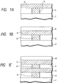
- Fig. 1 gives schematic cross-sectional views showing the single crystal forming method of the present invention, applied to formation of wirings.
- a substrate 1 composed for example of monocrystalline Si
- an insulation film 2 composed for example of silicon oxide
- a monocrystalline Al 3 serving as a seed
- an Al layer 4 to be converted into monocrystalline state by the method to be explained later.
- the insulation film 2 is formed on the substrate 1.
- Said insulation film can be composed, for example, of a silicon oxide film, a silicon nitride film or a silicon oxinitride film such as NSG, PSG, BSG or BPSG. These films can be formed by thermal oxidation, CVD or sputtering already known.
- monocrystalline Al (first Al) 3 is formed in the via hole.
- the above-explained Al-CVD method may be employed to form monocrystalline Al selectively in said via hole.
- the substrate surface temperature in this operation is in a range at least equal to the decomposition temperature of alkylaluminum hydride but not exceeding 450°C, more preferably from 260° to 440°C, and most preferably from 270° to 350°C.
- monocrystalline Al has satisfactory interface with the underlying Si, and also has satisfactory surface properties.
- non-monocrystalline Al (second Al) 4 is formed on the monocrystalline Al 3 and on the insulation film 2.
- the insulation film 2 constituting an electron non-donating surface
- a surface modifying step such as supply of ions or electrons by plasma, plasma damage or ion implantation to obtain a practically electron-donating surface.
- the non-monocrystalline Al can be formed also on the insulation film by the introduction of such surface modifying step (Fig. 1A).
- the heat treatment to be explained later is conducted to convert the non-monocrystalline Al into a monocrystalline state.
- Said heat treatment may be conducted at this point, or after the formation of an insulation film 5.
- said heat treatment may be conducted after the non-monocrystalline Al, to be converted into monocrystalline state, is patterned into the form of desired wirings, or prior to said patterning.
- the insulation film 5 is formed after the patterning of Al 4, as shown in Fig. 1B.
- Said insulation film 5 may be formed, like the insulation film 2, by CVD or sputtering.
- the wirings consisting of monocrystalline Al can be obtained in this manner.
- FIG. 1C there are shown an interlayer insulation film 5, selectively deposited monocrystalline Al 6, Al 7 in converted monocrystalline state, and a protective insulation film 8.
- the metal principally composed of Al is limited to pure aluminum, but it is also possible to convert Al containing Si in a small amount, for example 1 %, namely Al-Si, to monocrystalline state.
- the monocrystalline Al-Si seed can be formed, in the aforementioned Al-CVD method, by introducing Si-containing gas such as SiH4 or Si2H6 together with alkylaluminum hydride gas and hydrogen gas.
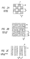
- Fig. 2 shows examples of arrangement of monocrystalline Al seeds.
- apertures of a lateral length of L1 are formed in a checkered pattern in an insulation film 11, formed for example on a Si surface, and monocrystalline Al is selectively deposited in said apertures.
- An unrepresented non-monocrystalline Al film is formed on the insulation film 11 and on the monocrystalline Al in the apertures 12, and is converted into monocrystalline state by heating, utilizing the monocrystalline Al as the seeds.
- apertures of a lateral length L2 are formed as via hole pattern with an interval L3, and, in an example in Fig.
- a line-and-space pattern is formed by insulators 11 of a width L5 and apertures 12 of a width L4.
- the monocrystalline Al is deposited selectively in the apertures, and an unrepresented non-monocrystalline Al film is formed, covering the monocrystalline Al and the insulator.
- the non-monocrystalline Al film is converted into monocrystalline state, utilizing the monocrystalline Al as the seeds.
- the basic procedure consists of preparing a specimen of a cross section as shown in Fig. 1A or 1B, and subjecting said specimen to heating step. Observations were made with X-ray diffraction, conventional RHEED and scanning ⁇ -RHEED microscope, before and after the heating.
- the transition of the second Al from the polycrystalline state to the monocrystalline state by heating is ascribed to the rearrangement of Al atoms, based on the increased flowability thereof. It is already known that a semiconductor containing a covalent bonding such as Si or GaAs present on a thin insulation film can be converted into monocrystalline state by heating.
- an Al or Al-Si film, present on an insulation film can be grown into polycrystals consisting of crystal grains of several microns by a heat treatment of 450°C, but the present invention is based on a finding that Al or Al-Si present on an insulator can be converted into monocrystalline state over an area in excess of 10 ⁇ m if a monocrystalline Al area is present under such Al or Al-Si film.
- Heating of the specimen can be achieved, for example, by heating in an electric oven with an atmosphere of H2, N2 or Ar or a mixture thereof, heating in vacuum, heating with a rapid thermal annealer (RTA), heating with a laser, heating with a linear heater such as a carbon heater, high frequency heating, lamp heating or electron beam heating.
- RTA rapid thermal annealer
- a pure Al film or an Al-Si film formed on Si reacts, when heated, with Si thereby causing erosion of the Si substrate or a leak in the Si pn junction present below the Al or Al-Si film.
- the heating treatment should preferably be conducted at a temperature as low as possible.
- the Al atoms have to become flowable by thermal energy. Consequently the heating method is preferably such as to heat the Al or Al-Si alone but not the Si substrate present thereunder.
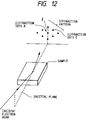
- Heating in vacuum can be achieved, in a scanning ⁇ -RHEED microscope shown in Fig. 3, by a heater positioned behind the substrate.
- FIG. 3 there are shown an electron gun 20; an electron beam 21; a diffracted electron beam 22; a fluorescent plate 23; optical fibers 24, 24′, 24 ⁇ ; photomultipliers 25, 25′, 25 ⁇ ; diffraction spot intensity signals 26, 26', 26" converted into electrical signals; a scanning signal 27; a cathode ray tube (CRT) 28; a secondary electron signal 29; a secondary electron detector 30; a specimen 31; a vacuum chamber 34; and a vacuum system 35.
- CTR cathode ray tube
- a specimen as shown in Fig. 1A is placed in the vacuum chamber 34, and is heated from the back by a heater 32.
- the temperature of the specimen is measured from the back thereof by a thermocouple 33.
- the heating may also be conducted by a lamp or a laser instead of the heater.
- the vacuum chamber 34 is evacuated by the vacuum system 35, to a level of 5 x 10 ⁇ 10 Torr prior to heating, and to a level of 5 x 10 ⁇ 9 - 5 x 10 ⁇ 8 Torr during the heating. Though a higher vacuum level is preferable, the conversion to monocrystalline state by heating is still possible even at a higher pressure than stated above.
- thermocouple 32 The transformation of aluminum to the monocrystalline state takes place when the temperature measured by the thermocouple 32 is about 550°C or higher.
- RTA rapid thermal annealer
- the RTA can heat solely the wafer surface within a short period, thereby minimizing the reaction of Al or Al-Si with the Si substrate.
- Fig. 4 shows an example of the RTA.
- a substrate 200 is supported by fingers 205 of a quartz substrate support 201.
- a quartz tube 202 may have a circular or square cross section, or may be replaced by a metal tube, such as a stainless steel tube, equipped with a quartz window.
- a linear lamp 203 of which light is reflected by a reflector 204 and irradiates the specimen 200 whose Al deposition face is directed to said lamp, may be composed of a halogen lamp, tungsten lamp, a Xe lamp or a Xe-Hg lamp. In the present example there is employed a halogen lamp of a higher heating speed.
- the internal atmosphere can be H2, N2 or Ar, or a mixture thereof.
- the H2 atmosphere is most preferred because highly pure gas, low in contents of moisture and oxygen, is available.
- a heating temperature of ca. 550°C or higher was necessary for the transformation to monocrystalline state.
- the substrate temperature was measured at the surface thereof, by means of a radiation thermometer utilizing PbS as a detector.
- Laser heating can also heat the substrate surface only, and has an advantage of providing a wider monocrystalline area than with the RTA.
- the laser employable for this purpose can be an argon ion laser (hereinafter represented as Ar laser), a krypton ion laser (hereinafter represented as Kr laser), a He-Ne laser, a CO2 laser, a YAG laser, an excimer laser such as ArF, KrF, XeF or XeCl laser with an output of several to twenty watts.
- the oscillation frequency can be continuous oscillation or pulsed oscillation of ca. 10 - 100 Hz.
- the laser heating is featured by a fact that the monocrystalline area can be enlarged by scanning of the specimen with the laser beam. Such enlargement of the monocrystalline area by laser scanning will be explained in the following.
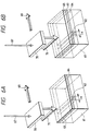
- Said specimen is scanned with a laser beam 67 in reciprocating manner as indicated by a line 68 in Fig. 5A, 5B or 7A, or in one direction as indicated by a line 69 in Fig. 6A, 6B or 7B.
- the laser beam is obtained from a continuously oscillated Ar laser or a pulse oscillated XeCl excimer laser and is focused to about 20 - 100 ⁇ m.
- a laser beam of a circular cross section is converted into a parallel beam 71 by an optical system 70 employing a cylindrical lens.
- the scanning direction of such laser beam or parallel laser beam is substantially perpendicular to the line of the first Al 62, as shown in Fig. 5A, 5B, 6A, 6B, 7A or 7B.
- a thermally oxidized SiO2 layer of a thickness of ca. 7000 ⁇ is formed on the Si substrate, with a line width L10 of ca. 10 ⁇ m for the first Al 62 and with a thickness of ca. 5000 ⁇ for the second Al 63, the beam from an Ar laser is converted into a parallel beam 71 and the specimen is scanned in one direction 69 with a speed of ca. 1 cm/sec. The rear face of the specimen is not heated.
- the Ar laser has an output of ca. 20 - 50 W, with a power density of ca. 50 - 200 Kw/cm2 on the specimen.
- the atmosphere of laser heating is H2 gas of 1 atmosphere.
- the substrate temperature is measured at the position of irradiation, with a radiation thermometer employing a PbS detector.
- the transformation to the monocrystalline state of Al on the first insulation film takes place when the substrate temperature is ca. 500°C or higher.
- Fig. 8 illustrates the method of heating with a linear heater.
- the substrate 82 to be heated is placed on a substrate support 81, made of carbon.
- a linear heater 83 which is also of carbon and energized by a power source 84.
- the substrate support 81 is also heated by a heater (not shown) provided at the bottom side of said support.
- the linear heater 83 moves in a direction 85.
- the atmosphere at heating may assume any pressure from vacuum to atmospheric pressure, and is preferably composed of H2, N2 Ar or a mixture thereof in order to prevent the oxidation of Al surface. Single crystal formation is possible also in vacuum, but the structure of the apparatus is simpler when the atmospheric pressure is employed.
- the transformation of the second Al to monocrystalline state takes place immediately below the linear heater, when the substrate temperature immediately below the linear heater is ca. 550°C or higher.
- the substrate temperature is measured with a radiation thermometer employing a PbS detector.
- the feature of heating with such linear heater lies, as in the laser heating, in a fact that the area of monocrystalline transformation can be expanded by scanning the heated area.
- Fig. 9 illustrates the heating method with a lamp, wherein a substrate 92 to be heated is placed on a substrate support 91, made of carbon.
- a lamp 93 can be a mercury lamp, a Hg-Xe lamp, a Xe lamp or a Xe flash lamp, and preferably has a linear structure.
- the light from the lamp 93 is condensed by a reflector 94 so as to form a line on the substrate surface.
- the substrate support 91 is also heated by a heater (not shown) provided on the bottom side thereof.
- the heated area 95 moves on the substrate in a direction 96, by the movement of the lamp.
- the atmosphere at heating may assume any pressure from atmospheric pressure to vacuum, and is preferably composed of H2, N2, Ar or a mixture thereof, in order to prevent oxidation of the Al surface.
- the single crystal formation is possible also in vacuum, but the atmospheric pressure allows to employ a simpler structure of the apparatus.
- the transformation of the second Al to monocrystalline state takes place in the heated linear area 95, when the substrate temperature therein is ca. 550°C or higher.
- the substrate temperature is measured by a radiation thermometer employing a PbS detector.
- Fig. 10 illustrates the heating method by high frequency heating.
- a substrate 103 to be heated is placed on a substrate support 101, made of carbon. Quartz plates 102 are provided with a gap therebetween.
- the substrate support bearing the substrate thereon as shown in Fig. 10 is heated by a high frequency coil (not shown) positioned therearound. Since the quartz plates 102 are not heated by the high frequency, a part 104 of the substrate is heated to a highest temperature.
- the atmosphere at heating may assume any pressure from atmospheric pressure to vacuum, and is preferably composed of H2, N2, Ar or a mixture thereof, in order to prevent oxidation of the Al surface.
- the single crystal formation is also possible in vacuum, but the atmospheric pressure allows to simplify the structure of the apparatus.
- the pressure of the atmosphere is atmospheric pressure.
- the transformation of the second Al to monocrystalline state takes place in the linear heated area 104, when the substrate temperature therein is ca. 550°C or higher.
- the substrate temperature is measured with a radiation thermometer employing a PbS detector.
- Fig. 11 illustrates the heating method with an electron beam.
- An electron beam 113 from a filament 112 is focused in the form of a line on a substrate 111 to be heated, by means of a condensing coil 115, a scanning coil and deflecting plates 115′.
- a linear portion 114 is heated to a high temperature.
- the heated area 114 also moves on the wafer.
- the atmosphere of heating is preferably high vacuum in order to prevent oxidation of the Al surface.
- the transformation of Al to monocrystalline state takes place at a presure of ca. 10 ⁇ 6 Torr or lower.
- the moving speed of the substrate is ca. 0.5 - 10 cm/min.
- the substrate surface temperature in the heated area is measured with a radiation thermometer employing a PbS detector, and the monocrystalline transformation of Al takes place when said temperature is ca. 450°C or higher.
- the scanning ⁇ -RHEED microscope is disclosed in Extended Abstracts of the 21st Conference on Solid State Devices and Materials (1989) p.217 and Japanese Journal of Applied Physics Vol. 28, No. 11(1989) L2075.
- the conventional RHEED (reflection high energy electron diffraction) method is to irradiate the specimen surface with an electron beam at a shallow angle of 2 - 3° and to evaluate the crystallinity of the specimen surface from the diffraction pattern generated by the diffracted electron beam, but can only provide averaged information of the specimen surface, because the diameter of the electron beam is as large as 100 to several hundred ⁇ m.
- the diameter of the electron beam from the electron gun 20 is reduced to 0.1 ⁇ m, and the electron beam diffraction pattern from a specified small area on the specimen surface can be observed on the fluorescent plate 23. It is also possible to two-dimensionally scan the specimen surface with the electron beam 21, to guide the diffracted electron beam 22 to the fluorescent plate 23, to utilize the intensity change of an arbitrary diffraction spot on the diffraction pattern as image signals 26, 26′, 26 ⁇ , and to obtain a two-dimensional image (scanning ⁇ -RHEED image) of the specimen surface by the diffraction spot intensity change on the CRT 28.
- observation of a scanning ⁇ -RHEED image employing different diffraction spots A, C on the diffraction pattern as shown in Fig. 12 allows to separately display the crystal grains in which the lattice planes are parallel to the specimen surface, for example to a plane (100) but are rotated in said plane.
- Said diffraction spot A is on a line l on which a plane of the diffraction spots and a sagittal plane of the incident electron beam perpendicularly cross, while the diffraction spot C is not on said line l.
- the scanning ⁇ -RHEED image utilizing the diffraction spot A shows both the crystal grains x, y as high intensity areas, but the image utilizing the spot C shows only the crystal grain x as the high intensity area. Consequently observation of the scanning ⁇ -RHEED image utilizing the diffraction spots A and C as shown in Fig. 12 allows to identify whether the crystal in the observed area is polycrystalline including in-plane rotation or monocrystalline.
- X-ray diffraction and conventional RHEED observation proved the polycrystalline state, but were unable to identify the size of the crystal grains.
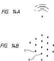
- Observation with a scanning ⁇ -RHEED microscope with an electron beam diameter reduced to 0.1 ⁇ m ⁇ provided a spot pattern shown in Fig. 14B though the intensity was weak.
- Fig. 15A shows the result of observation of the scanning ⁇ -RHEED image, utilizing the spot intensity variation on the diffraction pattern, wherein hatched areas indicate areas with a high diffraction spot intensity, while a white area indicates an area of weak intensity.
- the size of the hatched areas suggests that the size of the crystal grains is in the order of several to ten microns.
- Fig. 14B The spots in Fig. 14B were identified as a diffraction pattern generated when the electron beam is introduced from a direction [101] into the Al(111) plane.
- Figs. 15B and 15C indicate the results of observation of the scanning ⁇ -RHEED image, utilizing the intensity of a spot A (111 diffracted spot) and a spot C (202 diffracted spot) on the diffraction pattern in Fig. 14B.
- the monocrystalline transformation was also experimented with another specimen, which, as shown in Fig. 16A, is composed of an Si substrate bearing thereon a thermal silicon oxide film of a thickness of 1 ⁇ m and having apertures formed by dry etching in said film to expose the Si surface.
- a checker pattern In an area I there is formed a checker pattern, a via hole pattern or a line-and-space pattern as shown in Fig. 2A, 2B or 2C, while an area II is entirely covered by SiO2 without such pattern.
- the substrate with SiO2 pattern as shown in Fig. 16A was at first subjected to deposition of the first Al selectively in the apertures by the CVD method utilizing DMAH and H2, and, after a surface modifying step, the second Al was deposited over the entire surface of the substrate.
- Figs. 16B and 16C show the results of observation of the scanning ⁇ -RHEED image, utilizing the intensity of a diffraction spot A (111 diffracted spot) and a diffraction spot C (202 diffracted spot) in the diffraction pattern shown in Fig. 14B.
- Figs. 16B and 16C show the results of observation of the scanning ⁇ -RHEED image, utilizing the intensity of a diffraction spot A (111 diffracted spot) and a diffraction spot C (202 diffracted spot) in the diffraction pattern shown in Fig. 14B.
- hatched areas indicate areas with high diffraction spot intensity, corresponding to (111) single crystal.
- Figs. 16B and 16C suggest that the monocrystalline area extended by about 10 ⁇ m from the area I including the apertures. It was therefore confirmed that the transformation to monocrystalline state by heat treatment extended by about 10 ⁇ m from the patterned area I, even in the absence of exposed Si under the Al film.
- the area of transformation to monocrystalline state by heat treatment was same as in Figs. 16B and 16C, regardless of the thickness of SiO2. Also within a range of 500 ⁇ to 1 ⁇ m of the thickness of the Al film deposited on SiO2, the area of transformation was same as in Figs. 16B and 16C.
- the area of monocrystalline transformation was measured in the following manner.
- an area III is provided with a checkered pattern, a via hole pattern or a line-and-space pattern as in the area I in Fig. 16A, while an area IV is provided with the first insulation film.
- the first Al and the second Al were formed on such substrate.
- the second Al in deposited state was polycrystals with grains of several to ten microns in size.
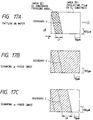
- the scanning is conducted in a direction x shown in Fig. 17A. Also in case of heating with a flat laser beam as shown in Fig. 6, or in case of lamp heating, high frequency heating or electron beam heating, the heated area is moved in said direction x.
- Figs. 17B and 17C show the results of observation with the scanning ⁇ -RHEED microscope after the heat treatment.
- the electron beam diffraction pattern by said microscope provided spots as shown in Fig. 14B, with increased intensity than before the heat treatment.
- the scanning ⁇ -RHEED observation, utilizing the intensity of a diffraction spot A (111 diffracted spot) and a diffraction spot C (202 diffracted spot) in the pattern shown in Fig. 14B provided images shown in Figs. 16B and 16C, wherein hatched areas indicate areas with high spot intensity.
- An area, where both spots A and C have high intensity, corresponds to (111) single crystal.
- a distance L8 indicates the area transformed to monocrystalline state by heat treatment.
- Fig. 17A illustrates the pattern of insulation film, corresponding to Figs. 17B and 17C.
- the above-mentioned specimen contains a stripe of the first Al in the area III, and the heated area is moved in the direction x shown in Fig. 17A.
- Fig. 17C shows L8 in a size of about 10 ⁇ m, but L8 reached ca. 1 cm in case of laser annealing, heating with linear heater, lamp heating, high frequency heating or electron beam heating.
- Electromigration resistance was measured on the Al film subjected to monocrystalline transformation on SiO2.
- the conventional Al or Al-Si wiring obtained by sputtering shows an average service life of 1 x 10² - 103 hours with a wiring cross section of 1 ⁇ m2, in a current test of 1 x 10⁶ A/cm2 at 250°C.
- the moncrystalline Al wiring of the present invention provided a service life of 104 - 105 hours with a cross section of 1 ⁇ m2 in the above-mentioned test.
- a wiring with a width of 0.8 ⁇ m and a thickness of 0.3 ⁇ m provided an average service life of 103 - 104 hours in said test.
- the percentage of wiring breakage was measured by patterning the monocrystalline Al into a width of ca. 1 ⁇ m, depositing a silicon nitride film thereon by a CVD method, and applying stress for 1000 hours at 150°C.
- the percentage of breakage in 1000 lines was 10 - 20 %, but, in the monocrystalline Al wiring of the present invention, no breakage was observed in 1000 lines.
- the monocrystalline Al wiring can drastically improve the resistance to electromigration and stress migration.
- Still another preferred embodiment of the present invention utilizes monocrystalline Al formed in a via hole which is formed in an insulation film as a seed crystal, and converts non-monocrystalline Al in other areas into monocrystalline state by heating. It is particularly preferable, after formation of monocrystalline Al by selective deposition of Al in the via hole, to non-selectively deposit Al also on the insulation film, and, after ion implantation, to apply heat treatment thereby converting Al on the insulation film into monocrystalline state. Such method allows to obtain a flat Al film, without formation of a recess in the Al film on the via hole.
- the non-monocrystalline Al film is once converted into amorphous or microcrystalline state, and is then transformed into monocrystalline state by heating, employing the monocrystalline Al as a seed crystal.
- the non-monocrystalline Al film formed as explained above, is subjected to the implantation of H+, Ar+, Si+ or Al+ ions by a known ion implanting method.
- H+, Ar+, Si+ or Al+ ions may also be employed, the above-mentioned four ions are preferably employed in order not to deteriorate the reliability of the Al or Al-Si wirings for ULSI, and Al+ or H+ ions are most preferable.
- Said H+, Al+, Ar+ or Si+ ions are preferably implanted with an acceleration voltage of ca. 50 kV or higher and with a dose of ca. 1 x 1015 cm ⁇ 2 or higher.
- the second Al can be converted into amorphous or microcrystalline state, even when said second Al has a thickness of ca. 5000 ⁇ .
- the ion implantation transforms Al, which is polycrystalline when deposited, into amorphous state. Since the Al atoms can more easily flow in the amorphous state than in the polycrystalline state, the transformation to monocrystalline state is achieved at a lower temperature than in the heat treatment at the polycrystalline state.
- a semiconductor having covalent bonds such as Si or GaAs on an insulating film is transformed into monocrystalline state by heat treatment.
- Si or GaAs on an insulating film is transformed into monocrystalline state by heat treatment.
- SPE single phase epitaxy
- silicon deposited on a monocrystalline Si substrate is converted into amorphous state by ion implantation, and is then converted to monocrystalline state by heat treatment for example in an electric oven.
- the present invention is based on a finding that even a metal film such as of Al present on an insulating film, after conversion into amorphous or microcrystalline state by ion implantation, can be transformed into monocrystalline state at a relatively low temperature. It is already known that an Al or Al-Si film on an insulating film can be grown into a polycrystalline film consisting of crystal grains of several microns by heat treatment of ca. 450°C. However transformation to the monocrystalline state by heat treatment has been impossible because the method of Al deposition for obtaining the structure shown in Fig. 1A has not been known, and also because the selectively deposited Al (first Al in Fig. 1A) has not been monocrystalline.
- the present invention has enabled, for the first time, to transform an Al film (second Al in Fig. 1A) on an insulating film into monocrystalline state by heat treatment after ion implantation, if selectively grown monocrystalline Al (first Al in Fig. 1A) is present thereunder.
- the semiconductor substrate is most preferably a Si substrate, but it may also be composed of GaAs, InP or Ge.
- the cross sectional structure of the specimen after formation of Al of Al-Si is as shown in Fig. 1A.
- the transformation to monocrystalline state is realized even if the second Al becomes thinner or thicker on the first Al.
- an insulation film 5 may be present on the second Al film as shown in Fig. 1B.
- Said insulation film 5 may be composed of SiO2 obtained by normal pressure CVD, phosphor-doped oxide film (PSG), borondoped oxide film (BSG), phosphor- and boron-doped oxide film (BPSG), silicon nitride film (SiN) obtained by low pressure CVD, or silicon nitride film obtained by ECR.
- Specimens were prepared with monocrystalline seed patterns as explained before, namely a checkered pattern as shown in Fig. 2A with L1 within a range of 0.5 - 20 ⁇ m, or a via hole pattern as shown in Fig. 2B with L3 of 20 ⁇ m or less, or a line-and-space pattern with L5 of 20 ⁇ m, and also with non-monocrystalline Al on such monocrystalline seed pattern.
- X-ray diffraction and conventional RHEED observation proved the polycrystalline state, but were unable to identify the size of the crystal grains.
- Observation with a scanning ⁇ -RHEED microscope with an electron beam diameter reduced to 0.1 ⁇ m ⁇ provided a spot pattern shown in Fig. 14B though the intensity was weak.
- Fig. 15A shows the result of observation of the scanning ⁇ -RHEED image, utilizing the spot intensity variation on the diffraction pattern, wherein hatched areas indicate areas with a high diffraction spot intensity, while a white area indicates an area of weak intensity.
- the size of the hatched areas suggests that the size of the crystal grains is in the order of several to ten microns.
- Said specimen was implanted for example with Al+ ions with an acceleration voltage of 50 kV and with a dose of 1 x 10¹⁶ /cm2.
- Said ion implantation caused transformation of the second Al into amorphous or microcrystalline state. Said transformation was confirmed in the following manner.
- the X-ray diffraction showed a diffraction peak of Al(111) in the deposited state, but, after ion implantation, no longer showed diffraction peak for aluminum.
- observation of the electron beam diffraction pattern by the conventional RHEED apparatus did not show circular nor spot pattern but so-called hallow pattern, indicating that the Al or Al-Si film was transformed by the ion implantation into a state which is not monocrystalline nor polycrystalline but amorphous or microcrystalline.
- Fig. 14B The spots in Fig. 14B were identified as a diffraction pattern generated when the electron beam is introduced from a direction [101] into the Al(111) plane.
- Figs. 15B and 15C indicate the results of observation of the scanning ⁇ -RHEED image, utilizing the intensity of a spot A (111 diffracted spot) and a spot C (202 diffracted spot) on the diffraction pattern in Fig. 14B.
- the monocrystalline transformation was also experimented with another specimen, which, as shown in Fig. 16A, is composed of an Si substrate bearing thereon a thermal silicon oxide film of a thickness of 1 ⁇ m and having apertures formed by dry etching in said film to expose the Si surface.
- a checkered pattern In an area I there is formed a checkered pattern, a via hole pattern or a line-and-space pattern as shown in Fig. 2A, B or C, while an area II is entirely covered by SiO2 without such pattern.
- the substrate with SiO2 pattern as shown in Fig. 16A was at first subjected to deposition of the first Al selectively in the apertures by the CVD method utilizing DMAH and H2, and, after a surface modifying step, the second Al was deposited over the entire surface of the substrate.
- Figs. 16B and 16C show the results of observation of the scanning ⁇ -RHEED image, utilizing the intensity of a diffraction spot A (111 diffracted spot) and a diffraction spot C (202 diffracted spot) in the diffraction pattern shown in Fig. 14B.
- Figs. 16B and 16C show the results of observation of the scanning ⁇ -RHEED image, utilizing the intensity of a diffraction spot A (111 diffracted spot) and a diffraction spot C (202 diffracted spot) in the diffraction pattern shown in Fig. 14B.
- hatched areas indicate areas with high diffraction spot intensity, corresponding to (111) single crystal.
- Figs. 16B and 16C suggest that the monocrystalline area extended by about 10 ⁇ m from the area I containing the apertures. It was therefore confirmed that the transformation to monocrystalline state by heat treatment extended by about 10 ⁇ m from the patterned area I, even in the absence of exposed Si under the Al film.
- the area of transformation to monocrystalline state by heat treatment was same as in Figs. 16B and 16C, regardless of the thickness of SiO2. Also with a range of 500 ⁇ to 1 ⁇ m of the thickness of the Al film deposited on SiO2, the area of transformation was same as in Figs. 16B and 16C.
- Electromigration resistance was measured on the Al film subjected to monocrystalline transformation on SiO2.
- the conventional Al or Al-Si wiring obtained by sputtering shows an average service life of 1 x 10² - 103 hours with a wiring cross section of 1 ⁇ m2, in a current test of 1 x 10⁶ A/cm2 at 250°C.
- the monocrystalline Al wiring of the present invention provided a service life of 104 - 105 hours with a cross section of 1 ⁇ m2 in the above-mentioned test.
- a wiring with a width of 0.8 ⁇ m and a thickness of 0.3 ⁇ m provided an average service life of 103 - 104 hours in said test.
- the percentage of wiring breakage was measured by patterning the monocrystalline Al into a width of ca. 1 ⁇ m, depositing a silicon nitride film thereon by a CVE method, and applying stress for 1000 hours at 150°C.
- the percentage of breakage in 1000 lines was 10 - 20 %, but, in the monocrystalline Al wiring of the present invention, no breakage was observed in 1000 lines.
- the monocrystalline Al wiring obtained after conversion to amorphous or microcrystalline state can drastically improve the resistance to electromigration and stress migration.
- the specimen used in the measurement having a cross-sectional structure as shown in Fig. 1A, was prepared in the following manner.
- Si wafer was subjected to thermal oxidation at 1000°C by hydrogen combustion (H2: 4 l/min., 02: 2 l/min.).
- the surface orientation of the Si wafer was (100) or (111).
- the entire wafer was coated with photoresist and was exposed to a desired pattern by an exposure apparatus. After the photoresist was developed, reactive ion etching was conducted, utilizing the photoresist as a mask, to etch the underlying SiO2, thereby locally exposing the Si surface.
- an Al film was deposited by a low pressure CVD method, employing dimethylaluminum hydride and hydrogen, with a deposition temperature of ca. 270°C and a pressure of ca. 1.5 Torr in the reactor tube.
- first Al selective Al deposition
- second Al was deposited on the entire surface.
- the SiO2 film thickness was varied in 5 levels of 1000, 2500, 5000, 7500 and 10000 ⁇ .
- the checkered pattern shown in Fig. 2A was used on the Si wafer, with size L1 varied in 8 levels of 0.25, 0.5, 1, 2, 3, 5, 10 and 20 ⁇ m.
- Thickness of the Al film deposited on the entire surface was varied in 5 levels of 1000, 2500, 5000, 7500 and 10000 ⁇ .
- the heating in the scanning ⁇ -RHEED microscope was varied in 5 levels of (1) 550°C, 6 hrs., (2) 600°C, 2 hrs., (3) 645°C 15 min., (4) 670°C, 5 min., and (5) 700°C, 5 min.
- the electron diffraction pattern and the scanning ⁇ -RHEED image were observed. All the specimens showed spot patterns as shown in Fig. 14B with higher intensity than before heating, regardless of the wafer surface orientation, SiO2 film thickness, checkered pattern size or second Al film thickness.
- the diffractin pattern shown in Fig. 14B was identified, from the spot positions, to be generated when the electron beam was introduced from a direction [101] into the Al(111) plane.
- the scanning ⁇ -RHEED image obtained utilizing the intensity of the diffracted spot A (111 diffracted spot) and spot C (202 diffracted spot) of the diffracted pattern in Fig.
- Specimens with a cross-section as shown in Fig. 1A were prepared in the same manner as in the example 1, and were heat treated in the scanning ⁇ -RHEED microscope.
- the via hole pattern shown in Fig. 2B was formed on the Si wafer, with L2 varied in 5 levels of 0.25, 0.5, 1, 2 and 5 ⁇ m and L3 in 5 levels of 1, 2, 5, 10 and 20 ⁇ m.
- L2 varied in 5 levels of 0.25, 0.5, 1, 2 and 5 ⁇ m
- L3 in 5 levels of 1, 2, 5, 10 and 20 ⁇ m.
- the thickness of the SiO2 film and of the Al film (second Al 4 in Fig. 1) deposited over the entire surface were same as those in the example 1.
- the specimens prepared as explained above were subjected to heat treatment and observations as in the example 1.
- the heat treating conditions were same as those in the example 1.
- the Al deposited on the entire surface was identified as polycrystals with an orientation (111) consisting of crystal grains of several to ten microns, as in example 1.
- the specimens were subjected to the observation of electron diffraction pattern and the scanning ⁇ -RHEED image. All the specimens showed, as in the example 1, spot patterns as shown in Fig. 14B with a higher intensity than before the heating, regardless of the wafer surface orientation, SiO2 film thickness, via hole dimensions and second Al film thickness.
- the scanning ⁇ -RHEED images utilizing the intensities of the diffracted spot A (111 diffracted spot) and C (202 diffracted spot) on the pattern shown in Fig. 14B were similar to those shown in Fig. 15B and 15C, as in the example 1.
- the Al film deposited in the area of via hole pattern showed strong intensities for both spots A and C, indicating transformation to monocrystalline state by the heat treatment.
- Specimens with a cross-section as shown in Fig. 1A were prepared in the same manner as in the example 1, and were heat treated in the scanning ⁇ -RHEED microscope.
- the line-and-space pattern shown in Fig. 2C was formed on the Si wafer, with L4 varied in 5 levels of 0.25, 0.5, 1, 2 and 5 ⁇ m, and L5 in 5 levels of 1, 2, 5, 10 and 20 ⁇ m.
- L4 varied in 5 levels of 0.25, 0.5, 1, 2 and 5 ⁇ m
- L5 in 5 levels of 1, 2, 5, 10 and 20 ⁇ m.
- the thicknesses of the SiO2 film and of the Al film (second Al 4 in Fig. 1) deposited over the entire surface were same as those in the example 1.
- the specimens thus prepared were subjected to the heat treatment and observations in the same manner as in the example 1.
- the heat treating conditions were also same as those in the example 1.
- the Al deposited on the entire surface (second Al) in all the specimens was identified, as in the example 1, as polycrystals of an orientation (111), consisting of crystal grains of several to ten microns.
- Specimens with a cross-section as shown in Fig. 1A were prepared in the same manner as in the example 1, and were heat treated in the scanning ⁇ -RHEED microscope.
- the SiO2 film is provided with apertures in an area I but is free from such apertures in an area II.
- the pattern in the area I was the checkered pattern, via hole pattern or line-and-space pattern shown in Fig. 2A, 2B or 2C.
- the size L1 was varied in 6 levels of 0.25, 0.5, 1, 2, 3 and 5 ⁇ m.
- L2 was varied in 5 levels of 0.25, 0.5, 1, 2 and 5 ⁇ m while L3 was varied in 3 levels of 1, 2 and 5 ⁇ m, and 15 different patterns were prepared by the combinations of L2 and L3.
- L4 was varied in 4 levels of 0.25, 0.5, 1 and 2 ⁇ m while L5 in 3 levels of 1, 2 and 5 ⁇ m, and 12 different patterns were prepared by the combinations of L4 and L5.
- the thicknesses of the SiO2 film and of the Al film deposited on the entire surface were same as those in the Example 1.
- the Al deposited on the entire surface (second Al) in all the specimens was identified as polycrystals with an orientation (111), consisting of crystal grains of several to ten microns.
- the insulation film was composed of SiO2 obtained by thermal oxidation.
- CVD SiO2 normal pressure CVD
- BSG normal pressure CVD
- PSG phosphor-doped oxide film obtained by normal pressure CVD
- BPSG normal pressure CVD
- P-SiN plasma CVD
- T-SiN thermal nitride film
- L-SiN thermal nitride film obtained by low pressure CVD
- ECR-SiN ECR apparatus
- the thickness of the insulation films was selected as ca. 5000 ⁇ , except that the thermal nitride film (T-SiN) was made with a thickness of ca. 100 ⁇ .
- the thickness of the second Al film was selected as ca. 7500 ⁇ . Formed patterns were same as those in the examples 1, 2, 3 and 4.
- the first and second Al films were both prepared by low pressure CVD.
- the second Al film was prepared by sputtering, but other conditions were maintained same as in the examples 1, 2, 3, 4 and 5.
- the first and second Al films were both composed of pure aluminum.
- pure aluminum was replaced by Al-Si, with Si content varied as 0.2, 0.5 or 1.0 %.
- the Al deposited on the entire surface (second Al) in all the specimens was identified as polycrystals with an orientation (111), consisting of crystal grains of several to ten microns.
- the heat treated specimens were subjected to the observations of the electron beam diffraction pattern and the scanning ⁇ -RHEED image in the scanning ⁇ -RHEED microscope shown in Fig. 3. All the specimens showed the spot electron beam diffraction patterns as shown in Fig. 14B, with a higher intensity than before the heat treatment, regardless of the Si wafer surface orientation, SiO2 film thickness, checkered pattern size or second Al film thickness.
- the diffraction pattern shown in Fig. 14B was identified, from the position of the diffraction spots, to be generated by the electron beam introduced from a direction [101] into the Al(111) plane.
- the scanning ⁇ -RHEED images, utilizing the intensity of the diffraction spot A (111 diffracted spot) and spot C (202 diffracted spot) on the diffraction pattern in Fig. 14B were similar to those shown in Figs. 15A and 15C, wherein hatched areas indicate those with high diffraction spot intensity.
- the Al film deposited on the checker-patterned area showed high intensities for both the spots A and C, indicating transformation to the monocrystalline state by heat treatment. Also in the observation of the electron diffraction pattern in the conventional RHEED apparatus, all the specimens after the heat treatment showed spot patterns as shown in Fig. 14B indicating the monocrystalline state.
- the Al film on SiO2 was transformed into monocrystalline state but showed unevenness in the thickness after the heat treatment. Also the measurements of element distribution in the direction of depth by electron spectroscopy for chemical analysis (ESCA) and Auger electron spectroscopy (AES), the specimen heat treated at 650°C showed diffusion of Al, Si and O at the interface between SiO2 and second Al film. Also transformation to monocrystalline state did not occur by the heat treatment at 500°C or lower.
- ESA electron spectroscopy
- AES Auger electron spectroscopy
- Specimens with via hole pattern shown in Fig. 2B were prepared as in the example 2, and subjected to heat treatment in the RTA apparatus.
- the sizes of the via holes were same as in the example 2.
- the A1 deposited on the entire surface (second Al) in all the specimens was identified as polycrystals with an orientation (111), consisting of crystal grains of several to ten microns.
- the Al film on SiO2 was transformed into monocrystalline state but showed unevenness in the thickness after the heat treatment. Also the measurements of element distribution in the direction of depth by electron spectroscopy for chemical analysis (ESCA) and Auger electron spectroscopy (AES), the specimen heat treated at 650°C showed diffusion of Al, Si and O at the interface between SiO2 and second Al film. Also transformation to monocrystalline state did not occur by the heat treatment at 500°C.
- ESA electron spectroscopy
- AES Auger electron spectroscopy
- Specimens were prepared with the line-and-space patterns as in the example 3 and subjected to heat treatment in the RTA apparatus.
- the specimens were subjected to heat treatment and observations in the same manner as in the example A1.
- the heat treating conditions were same as those in the example A1.
- the Al deposited on the entire surface (second Al) in all the specimens was identified as polycrystals with an orientation (111), consisting of crystal grains of several to ten microns.
- the Al film on SiO2 was transformed into monocrystalline state but showed unevenness in the thickness after the heat treatment. Also the measurements of element distribution in the direction of depth by electron spectroscopy for chemical analysis (ESCA) and Auger electron spectroscopy (AES), the specimen heat treated at 650°C showed diffusion of Al, Si and O at the interface between SiO2 and second Al film. Also transformation to monocrystalline state did not occur by the heat treatment at 500°C.
- ESA electron spectroscopy
- AES Auger electron spectroscopy
- Specimens with a cross-section as shown in Fig. 1A were prepared in the same manner as in the example 1 or A1, and were heat treated in the scanning ⁇ -RHEED microscope.
- the SiO2 film is provided with apertures in an area I but is free from such apertures in an area II.
- the pattern in the are I was the checkered pattern, via hole pattern or line-and-space pattern shown in Fig. 2A, 2B or 2C.
- the size L1 was varied in 6 levels of 0.25, 0.5, 1, 2, 3 and 5 ⁇ m.
- L2 was varied in 5 levels of 0.25, 0.5, 1, 2 and 5 ⁇ m while L2 in 3 levels or 1, 2 and 5 ⁇ m, and 15 different patterns were prepared by the combinations of L2 and L3.
- L3 was varied in 4 levels of 0.25, 0.5, 1 and 2 ⁇ m while L5 in 3 levels of 1, 2 and 5 ⁇ m, and 12 different patterns were prepared by the combinations of L4 and L5.
- the thicknesses of the SiO2 film and of the Al film deposited on the entire surface (second Al film 4 in Fig. 1A) were same as those in the example A1.
- the Al deposited on the entire surface (second Al) in all the specimens was identified as polycrystals with an orientation (111), consisting of crystal grains of several to ten microns.
- the Al film on SiO2 was transformed into monocrystalline state but showed unevenness in the thickness after the heat treatment. Also the measurements of element distribution in the direction of depth by electron spectroscopy for chemical analysis (ESCA) and Auger electron spectroscopy (AES), the specimen heated treated at 650°C showed diffusion of Al, Si and O at the interface between SiO2 and second Al film. Also transformation to monocrystalline state did not occur by the heat treatment at 500°C.
- ESA electron spectroscopy
- AES Auger electron spectroscopy
- the first insulation film was composed of SiO2 obtained by thermal oxidation.
- CVD SiO2 normal pressure CVD
- BSG normal pressure CVD
- PSG phosphor-doped oxide film obtained by normal pressure CVD
- BPSG normal pressure CVD
- P-SiN plasma CVD
- T-SiN thermal nitride film
- L-SiN thermal nitride film obtained by low pressure CVD
- ECR-SiN ECR apparatus
- the thickness of the first insulation films was selected as ca. 5000 ⁇ , except that the thermal nitride film (T-SiN) was made with a thickness of ca. 100 ⁇ .
- the thickness of the second Al film was selected as ca. 7500 ⁇ . Formed patterns were same as those in the examples A1, A2, A3 and A4.
- the first and second Al films were both prepared by low pressure CVD.
- the second Al film was prepared by sputtering, but other conditions were maintained same as in the examples A1, A2, A3, A4 and A5.
- the first and second Al films were both composed of pure aluminum.
- pure aluminum was replaced by Al-Si, with Si content varied as 0.2, 0.5 or 1.0 %.
- the specimens had the cross-sectional structure as shown in Fig. 1A.
- the specimens were subjected to the formation of a second insulation film 5 as shown in Fig. 1B, and to heat treatment in the RTA apparatus. Conditions were maintained same as in the examples A1 - A7, except for the cross-sectional structure.
- the crystallinity of the second Al film after the heat treatment was observed, after the removal of the second insulation film 5, by the conventional RHEED apparatus and the scanning ⁇ -RHEED microscope.
- the insulation film 5 in Fig. 1B was composed of SiO2, PSG, BSG or BPSG obtained by normal pressure CVD, silicon nitride film obtained by plasma CVD, or silicon nitride film obtained by ECR apparatus.
- the film thickness was varied in 3 levels of 1000, 3000 and 5000 ⁇ in each of said films.
- the Al deposited on the entire surface (second Al) in all the specimens was identified as polycrystals with an orientation (111), consisting of crystal grains of several to ten microns.
- the above-mentioned specimens were subjected to laser heating in the following manner. There was employed a continuously oscillated Ar laser (wavelength ca. 488 and 514.5 nm; maximum oscillation output: 20 W), with a beam diameter on the specimen of ca. 20, 30, 70 or 100 ⁇ m. There were conducted scanning motions repeated in one direction, as shown in Fig. 5A. The pitch of the scanning motions was selected approximately equal to the beam diameter. The scanning speed of the laser beam was ca. 0.5, 1, 2, 5 or 10 cm/min. The substrate surface temperature, measured with a radiation thermometer employed a PbS probe, was selected as ca. 450°, 550°, 600°, 650° or 700°C.
- the substrate surface temperature was dependent on the laser beam diameter, laser output and laser beam scanning speed.
- the laser output was so regulated as to obtain the surface temperature of ca. 450°, 550°, 600°, 650° or 700°C.
- the laser heating was conducted in hydrogen gas of atmospheric pressure.
- the scanning ⁇ -RHEED images obtained by utilizing the intensities of the diffraction spot A (111 diffracted spot) and spot C (202 diffracted spot) of the diffraction pattern in Fig. 14B were similar to those shown in Figs. 15B and 15C, wherein hatched areas indicate areas with high intensity of diffracted spots.
- the Al film deposited on the checker-patterned area showed high intensities for both spots A and C, indicating transformation to monocrystalline state by the heat treatment. Also in the observation of the heat treated specimen by the electron beam diffraction pattern by the conventional RHEED apparatus, all the specimens showed spot pattern indicating monocrystalline state, as shown in Fig. 14B.
- Specimens with checkered patterns were prepared in the same manner as in the example 2.
- the thicknesses of the SiO2 film and of the Al film deposited on the entire wafer surface were same as those in example 1.
- prepared specimens were subjected to the heat treatment and the observations in the same manner as in the example B1.
- the heat treating conditions were same as in the example B1.
- the Al deposited on the entire surface (second Al) in all the specimens was identified as polycrystals with an orientation (111), consisting of crystal grains of several to ten microns.
- heat treatment with laser beam irradiation was conducted in the same conditions as in the example B1, and there were conducted observations of the electron beam diffraction pattern and the scanning ⁇ -RHEED image.
- all the specimens treated at a surface temperature of 550°C or higher were confirmed to be transformed into monocrystalline state, regardless of the Si wafer surface orientation, SiO2 film thickness, checkered pattern size or second Al film thickness and also regardless of the laser beam diameter, scanning speed or scanning pitch.
- the specimens treated at a surface temperature of 650°C or higher showed diffusion of Si and Al at the interface of the insulation film on the substrate surface and the second Al film, as in the example 1.
- Specimens with a cross section as shown in Fig. 1A were prepared in the same manner as in the example B1 and were subjected to laser heating.
- the Al deposited on the entire surface (second Al) in all the specimens was identified as polycrystals with an orientation (111), consisting of crystal grains of several to ten microns.
- heat treatment with laser beam irradiation was conducted in the same conditions as in the example B1, and there were conducted observations of the electron beam diffraction pattern and the scanning ⁇ -RHEED image in the scanning ⁇ -RHEED microscope.
- all the speciments treated at a surface temperature of 550°C or higher were confirmed to be transformed into monocrystalline state, regardless of the Si wafer surface orientation, SiO2 film thickness, line-and-space pattern dimensions or second Al film thickness and also regardless of the laser beam diameter, scanning speed of scanning pitch.
- the specimens treated at a surface temperature of 650°C or higher showed diffusion of Si and Al at the interface between the insulation film on the substrate surface and the second Al film, as in the example B1.
- Specimens were prepared in the same manner as in the examples B1, B2 and B3.
- the present example is different from said examples in the shape of the laser beam and the scanning method thereof.
- the above-mentioned specimens were subjected to heating by a laser, which was a continuously oscillated Ar laser (wavelength ca. 488 and 514.5 nm).
- the beam on the specimen was a flat parallel beam as shown in Fig. 6A.
- a circular beam 67 was transformed into a parallel beam 71 by an optical system 70 employing a cylindrical lens.
- the shape of the parallel beam was ca. 20 ⁇ m x 1 cm, 50 ⁇ m x 1 cm or 100 ⁇ m x 1 cm.
- the scanning was conducted in one direction as shown in Fig. 6A, with a speed of ca. 0.5, 1, 2, 5 or 10 cm/min.
- the substrate surface temperature measured by a radiation thermometer employing a PbS probe, was selected at ca. 450°, 550°, 600°, 650° or 700°C.
- the substrate surface temperature was dependent on the shape, output and scanning speed of the laser beam.
- the laser output was so regulated as to obtain the surface temperature of ca. 450°, 550°, 600°, 650° or 700°C mentioned above.
- the laser heating was conducted in hydrogen gas of atmospheric pressure.
- the measurement of element distribution in the direction of depth by Auger electron spectroscopy or secondary ion mass spectroscopy showed the diffusion of Si and Al at the interface between the insulation film on the substrate surface and the second Al film, when the substrate surface temperature was 650°C or higher.
- the second Al film was formed on the entire surface of the specimen as shown in cross section in Fig. 1A.
- an insulation film 5 was formed on the specimens of the examples B1, B2 and B3, as shown in Fig. 1B, and the heat treatment with laser was conducted in the same manner as in said foregoing examples.
- the insulation film on the second Al film was composed of a SiO2 film obtained by normal pressure CVD (hereinafter expressed as CVD SiO2), a boron-doped oxide film obtained by normal pressure CVD (BSG), a phosphor-doped oxide film obtained by normal pressure CVD (PSG), a boron- and phosphor-doped oxide film obtained by normal pressure CVD (BPSG), a nitride film obtained by plasma CVD (P-SiN), or a nitride film obtained by CER apparatus (ECR-SiN).
- the insulation film on the second Al film will hereinafter be called the second insulation film.
- the thickness of said second insulation film was selected as 1000, 2000, 5000 or 10000 ⁇ .
- the laser heating conditions were same as in the examples B1, B2 and B3.
- the specimens were subjected to the removal of the second insulation film by etching and then subjected to the observations of the electron beam diffraction pattern and the scanning ⁇ -RHEED image in the scanning ⁇ -RHEED microscope, as in the examples B1, B2 and B3.
- the obtained results indicated that the second Al was transformed into monocrystalline state when the substrate temperature was 550°C or higher.
- the measurement of element distribution in the direction of depth by Auger electron spectroscopy or secondary ion mass spectroscopy indicated diffusion of Si and Al at the interface between the insulation film on the substrate surface and the second Al film when the substrate surface temperature was equal to 650°C or higher.
- the second Al film was formed on the entire surface of the specimen as shown in cross section in Fig. 1A.
- a second Al film was formed on the specimens of the example B4 as shown in Fig. 1B, and the laser heating was conducted in the same manner as in said example B4.
- the insulation film on the second Al film was composed of CVD SiO2, BSG, PSG, BPS, P-SiN or ECR-SiN. Said insulation film on the second Al film will hereinafter be called a second insulation film.
- the thickness of said second insulation film was selected as 1000, 2000, 5000 or 10000 ⁇ .
- the laser heating conditions were same as those in the example B4.
- the specimens were subjected to the removal of the second insulation film by etching, and to the observations of the electron beam diffraction pattern and the scanning ⁇ -RHEED image by the scanning ⁇ -RHEED microscope as in the example B4.
- the obtained results indicated, as in the example B4, that the second Al film was transformed into monocrystalline state when the substrate temperature was 550°C or higher.
- the measurement of element distribution in the direction of depth by Auger electron spectroscopy or secondary ion mass spectroscopy indicated the diffusion of Si and Al at the interface between the insulation film on the substrate surface and the second Al film, when the substrate surface temperature was 650°C or higher, as in the example B4.
- the insulation film formed on the Si substrate as shown in Fig. 1A was composed of SiO2, formed by thermal oxidation.
- the insulation film on the Si substrate was composed of CVD SiO2, BSG, PSG, BPSG, P-SiN, T-SiN, LP-SiN or ECR-SiN, with thicknesses of 5 levels of 1000, 2500, 5000, 7500 and 10000 ⁇ .
- the thicknesses of the first and second Al films, and the laser heating conditions were same as those in the examples B1, B2, B3 and B4.
- the second Al was transformed to monocrystalline state when the substrate temperature was 550°C or higher. Also as in said examples, the measurement of element distribution in the direction of depth by Auger electron spectroscopy or secondary ion mass spectroscopy indicated diffusion of Si and Al at the interface between the insulation film on the substrate surface and the second Al film, when the substrate surface temperature was 650°C or higher.
- the second Al film was formed over the entire surface of the specimen, as shown in cross section in Fig. 1A.
- an insulation film was formed on the second Al film of the specimens of the example B7, as shown in Fig. 1B, and the heat treatment with the laser beam was conducted in the same manner as in the example B7.
- the insulation film on the second Al was composed of CVD-SiO2, BSG, PSG, BPSG, P-SiN, T-SiN, LP-SiN or ECR-SiN, with a thickness varied in 5 levels of 1000, 2500, 5000, 7500 and 10000 ⁇ .
- the thicknesses of the first and second Al films and the laser heating conditions were same as in the examples B1, B2, B3 and B4.
- the second Al was transformed into monocrystalline state when the substrate temperature was 550°C or higher.
- the measurement of element distribution in the direction of depth by Auger electron spectroscopy or secondary ion mass spectroscopy indicated diffusion of Si and Al at the interface between the insulation film on the substrate surface and the second Al film, when the substrate surface temperature was 650°C or higher.
- the specimen had a structure schematically shown in Fig. 5A and a cross section shown in Fig. 1A.
- the insulation film on the Si substrate was provided with a line of a width L10, which was varied in 6 levels of 0.5, 1, 2, 5, 10 and 20 ⁇ m.
- the surface orientation of the Si substrate was selected as (100) or (111).
- the insulation film was composed of SiO2 obtained by thermal oxidation, with a thickness varied in 5 levels of 1000, 2500, 5000, 7500 and 10000 ⁇ .
- Al deposited over the entire surface (second Al 4 in Fig. 1A or second Al 63 in Fig.
- the second Al was identified as polycrystals consisting of crystal grains of several to ten microns, as in the example 1.
- the beam diameter on the specimen was ca. 20, 30, 70 or 100 ⁇ m, and the scanning was conducted in one direction in repeated manner as shown in Fig. 5A.
- the pitch of scanning was selected approximately same as the beam diameter.
- the scanning speed of the laser beam was ca. 0.5, 1, 2, 5 or 10 cm/min.
- the substrate surface temperature measured by a radiation thermometer employing a PbS probe, was selected as ca. 450°, 550°, 600°, 650° or 700 °C. The substrate surface temperature was dependent on the diameter, output and scanning speed of the laser beam.
- the laser output was so regulated as to obtain the above-mentioned surface temperature of ca. 450°, 550°, 600°, 650° or 700°C.
- the laser heating was conducted in hydrogen gas of atmospheric pressure.
- the electron diffraction pattern and the scanning ⁇ -RHEED image were observed in the scanning ⁇ -RHEED microscope.
- the electron diffraction pattern showed spots with a higher intensity than before the heat treatment, as in the example B1 (Fig. 14B).
- the scanning ⁇ -RHEED images obtained utilizing the 111 and 202 diffracted spots were similar to those shown in Figs. 17B and 17C.
- the direction of the first Al is parallel to y-direction in Fig. 17A, and the scanning direction of the laser beam is parallel to x-direction.
- the length of area transformed into monocrystalline state can be determined by measuring L8 in Fig. 17C. Though L8 is illustrated as about 10 - 20 ⁇ m in Fig.
- the second Al film on SiO2 was transformed into monocrystalline state over a length of 1 cm, utilizing monocrystalline first Al as the seed.
- the measurement of element distribution in the direction of depth by Auger electron spectroscopy or secondary ion mass spectroscopy indicated diffusion of Si and Al at the interface between the insulation film on the substrate surface and the second Al film, when the substrate surface temperature was 650°C or higher.
- Specimens were prepared in the same manner as in the example B9, and were subjected to heat treatment by laser.
- the specimens were different in the cross-sectional structure from those of the example B9.
- the second Al film was formed on the entire surface of the specimen as shown in Fig. 1A or 5A.
- an insulation film was formed on the second Al as shown in Fig. 1B or 5B, and the heat treatment with the laser beam was conducted in the same manner as in the example B9.
- the insulation film, hereinafter called the second insulation film, on the second Al was composed of CVD-SiO2, PSG, BSG, BPSG, P-SiN or ECR-SiN.
- the thickness of the second insulation film was selected as 1000, 2000, 5000 or 10000 ⁇ .
- the laser heating conditions were same as in the examples B1, B2 and B3.
- the second insulation film was removed by etching, and the electron beam diffraction pattern and the scanning ⁇ -RHEED image were observed in the scanning ⁇ -RHEED microscope.
- the measurement of element distribution in the direction of depth by Auger electron spectroscopy or secondary ion mass spectroscopy indicated diffusion of Si and Al at the interface between the insulation film on the substrate surface and the second Al film, when the substrate surface temperature was 650°C or higher.
- the specimens had a structure schematically shown in Fig. 6A and a cross section shown in Fig. 1B.
- the insulation film on the Si substrate was provided with a line of a width L10, and the dimensions of the specimens were same as in the example B9.
- the second Al was identified as polycrystals consisting of crystal grains of several to ten microns, as in the example B9.
- the above-mentioned specimens were subjected to heating by a laser, which was a continuously oscillated Ar laser (wavelength ca. 488 and 514.5 nm).
- the beam on the specimen was a flat parallel beam as shown in Fig. 6A.
- a circular beam was converted into a parallel beam by an optical system 70 employing a cylindrical lens.
- the shape of said parallel beam was ca. 20 ⁇ m x 1 cm, 50 ⁇ m x 1 cm or 100 ⁇ m x 1 cm.
- the scanning was conducted in one direction as shown in Fig. 6A, with a speed of ca. 0.5, 1, 2, 5 or 10 cm/min.
- the substrate surface temperature measured by a radiation thermometer employing a PbS probe, was selected at ca. 450°, 550°, 600°, 650° or 700°C.
- the substrate surface temperature was dependent on the shape, output and scanning speed of the laser beam.
- the laser output was so regulated as to obtain the above-mentioned surface temperature of ca. 450°, 550°, 600°, 650° or 700°C.
- the laser heating was conducted in hydrogen gas of atmospheric pressure.
- the electron diffraction pattern and the scanning ⁇ -RHEED image were observed in the scanning ⁇ -RHEED microscope.
- the electron diffraction pattern showed spots with a higher intensity than before the heat treatment as in the example B9 (Fig. 14B).
- the scanning ⁇ -RHEED images obtained utilizing the 111 and 202 diffracted spots were similar to those shown in Figs. 17B and 17C.
- the direction of the first Al was parallel to y-direction in Fig. 17A, and the scanning direction of the laser beam was parallel to x-direction.
- the length of area transformed to monocrystalline state can be determined by measuring L8 in Fig. 17C. Though L8 is illustrated as about 10 - 20 ⁇ m in Fig.
- the second Al film on SiO2 was transformed into monocrystalline state over a length of 1 cm, utilizing monocrystalline first Al as the seed.
- the measurement of element distribution in the direction of depth by Auger electron spectroscopy or secondary ion mass spectroscopy indicated diffusion of Si and Al at the interface between the insulation film on the substrate surface and the second Al film, when the substrate surface temperature was 650°C or higher.
- Specimens were prepared in the same manner as in the example B11, and were subjected to heat treatment by laser.
- the specimens were different in the cross-sectional structure from those of the example B11.
- the second Al film was formed on the entire surface of the specimen as shown in Fig. 1A or 5A.
- an insulation film was formed on the second Al as shown in Fig. 1B or 5B, and the heat treatment with the laser beam was conducted in the same manner as in the example B11.
- the insulation film, hereinafter called the second insulation film, on the second Al was composed of CVD-SiO2, PSG, BSG, BPSG, P-SiN or ECR-SiN.
- the thickness of the second insulation film was selected as 1000, 2000, 5000 or 10000 ⁇ . After the laser heating, the second insulation film was removed by etching, and the electron beam diffraction pattern and the scanning ⁇ -RHEED image were observed in the scanning ⁇ -RHEED microscope as in the example B11. The obtained results indicated, as in the example B11, that the second Al was transformed into monocrystalline state when the substrate temperature was 550°C or higher. Observation of the area transformed into monocrystalline state by the scanning ⁇ -RHEED image as in the example B11 provided similar results to those shown in Figs. 17B and 17C, with L8 of ca. 1 cm.
- the measurement of element distribution in the direction of depth by Auger electron spectroscopy or secondary ion mass spectroscopy indicated diffusion of Si and Al at the interface between the insulation film on the substrate surface and the second Al film, when the substrate surface temperature was 650°C or higher.
- the insulation film on the second Al was formed uniformly on the specimen in the example B10, but, in the present example, it was formed in stripes substantially perpendicular to the direction of the first Al (line direction) as shown in Fig. 7A.
- the second insulation film was composed of CVD-SiO2, PSG, BSG, BPSG, P-SiN or ECR-SiN, with a thickness of 1000, 2000, 5000 or 10000 ⁇ .
- the stripes of the second insulation film were formed in 16 different dimensions, by taking combinations of L14 as 1, 2, 5 and 10 ⁇ m and L15 as 1, 2, 5 and 10 ⁇ m.
- the laser heating conditions were same as those in the examples B1, B2 and B3. After the laser heating, the second insulation film was removed by etching, and the electron beam diffraction pattern and the scanning ⁇ -RHEED image were observed by the scanning ⁇ -RHEED microscope, as in the example B9.
- the scanning ⁇ -RHEED images observed in the area of monocrystalline transformation as in the example B9 were similar to those shown in Figs. 17B and 17C, with L8 being about 1 cm.
- the measurement of element distribution in the direction of depth by Auger electron spectroscopy or secondary ion mass spectroscopy indicated diffusion of Si and Al at the interface between the insulation film on the substrate surface and the second Al film, when the substrate surface temperature was 650°C or higher.
- Specimens were prepared in the same manner as in the example B13 and subjected to heat treatment by laser.
- This example is however different in the laser beam scanning method from said example B13.
- a continuously oscillated Ar laser (wavelength: ca. 488.5 and 415.5 nm) with a parallel flat beam on the specimen surface, as shown in Fig. 7B.
- a circular beam was converted into a parallel beam by an optical system 70 employing a cylindircal lens.
- the dimension of said parallel beam was ca. 20 ⁇ m x 1 cm, 50 ⁇ m x 1 cm or 100 ⁇ m x 1 cm, and the scanning was conducted in one direction as shown in Fig. 7B.
- the scanning speed was ca. 0.5, 1, 2, 5 or 10 cm/min.
- the substrate surface temperature measured with a radiation thermometer employing a PbS probe, was ca. 450°, 550°, 600°, 650° or 700°C.
- the substrate surface temperature was dependent on the shape, output and scanning speed of the laser beam.
- the laser output was so regulated as to obtain the above-mentioned surface temperature of ca. 450°, 550°, 600°, 650° or 700°C.
- the laser heating was conducted in hydrogen gas of atmospheric pressure.
- the obtained results indicated that the second Al was transformed into monocrystalline state when the substrate temperature was 550°C or higher.
- the scanning ⁇ -RHEED images observed in the monocrystalline area as in the example B13 were similar to those shown in Figs. 17B and 17C, with L8 being ca. 1 cm.
- the measurement of element distribution in the direction of depth by Auger electron spectroscopy or secondary ion mass spectroscopy indicated diffusion of Si and Al at the interface between the insulation film on (he substrate surface and the second Al film, when the substrate surface temperature was 650°C or higher.
- the insulation film formed on the Si substrate as shown in Figs. 5A, 5B, 6A, 6B, 7A or 7B was composed of SiO2 obtained by thermal oxidation.
- the insulation film on the Si substrate was CVD-SiO2, BSG, PSG, BPSG, P-SiN, T-SiN, LP-SiN or ECR-SiN, with a thickness of 1000, 2000, 5000, 7500 or 10000 ⁇ .
- the thicknesses of the first and second Al films were same as those in the examples B1, B2, B3 and B4.
- the monocrystalline transformation of the second Al film occurred when the substrate temperature was 550°C or higher.
- the measurement of element distribution in the direction of depth by Auger electron spectroscopy or secondary ion mass spectroscopy indicated diffusion of Si and Al at the interface between the insulation film on the substrate surface and the second Al film, when the substrate surface temperature was 650°C or higher.
- the first and second Al films were composed of pure aluminum obtained by the LP-CVD method utilizing DMAH (dimethylaluminum hydride) and hydrogen.
- pure aluminum was replaced by Al-Si, deposited by the addition of Si2H6 in the LP-CVD method utilizing DMAH and hydrogen.
- the Si content in the first and second Al-Si films was varied as 0.2, 0.5 or 1.0 %.
- the first and second Al films were both formed by the LP-CVD method employing DMAH and hydrogen.
- the first Al film has to be monocrystalline.
- Said LP-CVD method has the advantage of being capable of depositing the first and second Al films in succession in a same apparatus, but the second Al film need not be formed by a CVD method as long as it is polycrystalline or amorphous.
- the present example was conducted in the same manner as the examples B1 - B15, except that the second Al film alone was formed by sputtering. Based on the X-ray diffraction, electron beam diffraction pattern obtained by the conventional RHEED apparatus, and electron beam diffraction pattern and scanning ⁇ -RHEED image obtained by the scanning ⁇ -RHEED microscope, the second Al film in deposited state was identified as polycrystalline, consisting of crystal grains of about 1 ⁇ m or less.
- the specimen structure and the heating conditions were same as in the examples B1 - B15, but the first Al was composed of Al-Si formed by LP-CVD method employing DMAH, hydrogen and Si2H6, while the second Al was composed of pure aluminum formed by LP-CVD utilizing DMAH and hydrogen.
- the Si content in the first Al-Si film was selected as 0.2, 0.5 or 1.0 %.
- the specimen structure and the heating conditions were same as in the examples B1 - B15, but the first Al was composed of Al-Si formed by LP-CVD employing DMAH, hydrogen and Si2H6 while the second Al was composed of Al-Si formed by sputtering.
- the Si content in the first Al-Si film was selected as 0.2, 0.5 or 1.0 %.
- the heating was conducted by laser beam irradiation from the top surface of specimen.
- heating was conducted by heating from the bottom side of the specimen, in addition to the laser beam irradiation from the top surface.
- the bottom side heating was achieved by resistance heating of a specimen support (not shown).
- the temperature of the bottom surface of the specimen was selected as ca. 250, 300 or 350°C.
- the laser irradiating conditions were same as in the examples B1 - B19.
- Specimens with first and second Al films were prepared as explained in the examples 1, 2 and 3, and were heat treated with a linear heater.
- the first insulation film was patterned in the checkered pattern, via hole pattern and line-and-space pattern shown in Figs. 2A, 2B and 2C, with dimensions L1 - L5 same as in the examples B1 - B3.
- the surface orientation of the Si substrate and the thicknesses of the first insulation film and the second Al film were same as in the examples B1 - B3.
- Fig. 8 illustrates the heating method with the linear heater.
- the substrate 82 is placed on a heating support 81 made of carbon.
- a linear heater 83 which is also of carbon and is energized by a power source 84.
- the heating support 81 is also heated by a heater (not shown) provided on the bottom side thereof.
- the linear heater 83 moves in a direction 85. The heating was conducted in hydrogen gas of atmospheric pressure.
- the linear heater 83 was moved in the direction 85, with a speed of ca. 0.5, 1, 2, 5 or 10 cm/min.
- the substrate surface temperature directly below the linear heater 83 measured with a radiation thermometer employing a PbS probe, was ca. 450, 500, 600, 650 or 700°C.
- the electron beam diffraction pattern and the scanning ⁇ -RHEED image were observed in the scanning ⁇ -RHEED microscope. All the specimens showed spot patterns as shown in Fig. 14B, with a higher intensity than before the heating, regardless of the Si wafer surface orientation, SiO2 film (first insulation film) thickness, shape and size of the pattern, or second Al film thickness, as long as the substrate surface temperature directly below the linear heater 83 was 550°C or higher.
- the diffraction pattern in Fig. 14B was identified, from the position of the spots, as being generated by the electron beam introduced from a direction [101] into the Al (111) plane.
- the scanning ⁇ -RHEED images obtained utilizing the intensities of a diffraction spot A (111 diffracted spot) and a spot C (202 diffracted spot) in the pattern shown in Fig. 14B were similar to those shown in Fig. 15B and 15C, wherein areas of diffraction spots with high intensity are hatched.
- the Al film deposited on the checkered pattern, via hole pattern or line-and-space pattern (second Al film) provided high intensities both in the spots A and C, indicating the transformation to monocrystalline state by the heat treatment. Also in the electron beam diffraction pattern observed in the conventional RHEED apparatus after the heat treatment, all the specimens provided spot patterns indicating monocrystalline state as shown in Fig. 14B.
- the polycrystalline Al when deposited was transformed into monocrystalline state by heating.
- the transformation to monocrystalline state did not occur by heat treatment of 500°C, 6 hrs.
- the second Al film was formed on the entire surface of the specimen, as shown in cross section in Fig. 1A.
- an insulation film was formed on the second Al film at shown in Fig. 1B, and the heat treatment with the linear heater was conducted in the same manner as in the example C1.
- the insulation film on the second Al was composed of a SiO2 film obtained by normal pressure CVD (hereinafter represented as CVD-SiO2), a boron-doped oxide film obtained by normal pressure CVD (BSG), a phosphor-doped oxide film obtained by normal pressure CVD (PSG), a boron- and phosphor-doped oxide film obtained by normal pressure CVD (BPSG), a nitride film obtained by plasma CVD (P-SiN), or a thermal nitride film obtained by the ECR apparatus (ECR-SiN), with a thickness of 1000, 2000, 5000 or 10000 ⁇ .
- the heating conditions were same as in the example C1.
- the second insulation film was removed by etching, and the electron beam diffraction pattern and the scanning ⁇ -RHEED image were observed in the scanning ⁇ -RHEED microscope as in the example C1.
- the obtained results indicated, as in the example C1, that the second Al was transformed into monocrystalline state when the substrate temperature was 550°C or higher.
- the measurement of element distribution in the direction of depth, by Auger electron spectroscopy or secondary ion mass spectroscopy indicated the diffusion of Si and Al at the interface between the insulation film on the substrate surface and the second Al film, when the substrate surface temperature was 650°C or higher.
- the first insulation film formed on the Si substrate shown in Fig. 1A, was composed of SiO2 obtained by thermal oxidation.
- the first insulation film on the Si substrate was composed of CVD-SiO2, BSG, PSG, BPSG, P-SiN, T-SiN, LP-SiN or ECR-SiN, with a thickness of 1000, 2500, 5000, 7500 or 10000 ⁇ .
- the surface orientation of the Si substrate, thicknesses of the first and second Al films and heating conditions with the linear heater were selected same as in the example C1.
- the transformation of the second Al film into monocrystalline state occurred when the substrate temperature was 550°C or higher.
- the second Al was formed on the entire surface of the specimen as shown in cross section in Fig. 1A.
- an insulation film was formed on the second Al film as shown in Fig. 1B, and the heat treatment with the linear heater was conducted in the same manner as in the example C1.
- Said insulation film, on the second Al was composed of CVD-SiO2, BSG, PSG, BPSG, P-SiN, LP-SiN or EC-SiN, with thickness varied in 5 levels of 1000, 2500, 5000, 7500 and 10000 ⁇ .
- the surface orientation of the Si substrate, thicknesses of the first and second Al films, and heating conditions of the linear heater were same as in the example C3.
- the monocrystalline transformation of the second Al occurred when the substrate temperature was 550°C or higher.
- the specimen structure was as shown in Fig. 5A, and same as that in the example B9 employing laser heating, with a cross-sectional structure as shown in Fig. 1A.
- the insulation film on the Si substrate is provided with a line of width L10, which was varied in 6 levels of 0.5, 1, 2, 5, 10 and 20 ⁇ m.
- the surface orientation of the Si wafer was selected as (100) or (111).
- the insulation film was composed of SiO2 obtained by thermal oxidation, with thickness varied in 5 levels of 1000, 2500, 5000, 7500 and 10000 ⁇ . Also the thickness of the Al deposited on the entire surface (second Al 4 in Fig. 1, or second Al 63 in Fig.
- the second Al film was identified as polycrystals consisting of crystal grains of several to ten microns, as in the examples B1 and C1.
- the heating was conducted in the same manner as in the example C1, with a moving speed of ca. 0.5, 1, 2, 5 or 10 cm/min.
- the heating was conducted in hydrogen gas of atmospheric pressure.
- the electron beam diffraction pattern and the scanning ⁇ -RHEED image were observed in the scanning ⁇ -RHEED microscope.
- the electron beam diffraction patterns were dot patterns as shown in Fig. 14B, with intensities higher than before the heating, as in the example C1.
- the scanning ⁇ -RHEED images utilizing the intensities of the 111 and 202 diffracted spots were similar to those shown in Figs. 17B and 17C.
- the direction of first Al (line direction) is parallel to the y-direction in Fig. 17A, while the heater scanning direction is parallel to the x-direction.
- the length of the area transformed into monocrystalline state can be determined from the measurement of L8 in Fig. 17C. Though L8 in Fig.
- 17C is illustrated in the order of 10 - 20 ⁇ m, it was in fact about 1 cm when the substrate temperature was 550°C or higher.
- the second Al film on SiO2 was transformed into monocrystalline state over a length of 1 cm, utilizing monocrystalline first Al as the seed.
- Specimens were prepared in the same manner as in the example C5, and were heat treated with the linear heater. Said specimens were however different in cross-sectional structure from those in the example C5.
- the second Al film was formed on the entire surface of the specimen, as shown in cross section in Fig. 1A or 5A.
- an insulation film was formed on the second Al, as shown in Fig. 1B or 5B, and the heat treatment with the linear heater was conducted in the same manner as in the example C5.
- the insulatiln film on the second Al was composed of CVD-SiO2, PSG, BSG, BPSG, P-SiN or ECR-SiN, with a thickness of 1000, 2000, 5000 or 10000 ⁇ .
- the heating conditions with the linear heater were same as those in the example C1.
- the second insulation film was removed by etching, and the electron beam diffraction pattern and the scanning ⁇ -RHEED image were observed in the scanning ⁇ -RHEED microscope as in the example C5.
- the insulation film formed on the Si substrate in the structures shown in Figs, 5A and 5B, was composed of SiO2 obtained by thermal oxidation.
- the insulation film on the Si substrate was composed of CVD-SiO2, BSG, PSG, BPSG, P-SiN, T-SiN, LP-SiN or ECR-SiN, with thickness varied in 5 levels of 1000, 2500, 5000, 7500 and 10000 ⁇ .
- Surface orientation of the Si substrate, thicknesses of the first and second Al films, and heating conditions with the linear heater were same as those in the example C1.
- the second Al was transformed to monocrystalline state when the substrate temperature was 550°C or higher. Also as in the examples C5 and C6, there were obtained the scanning ⁇ -RHEED images similar to those in Figs. 17B and 17C, with the transformed monocrystalline area L8 of ca. 1 cm. Further, as in the examples C5 and C6, the measurement of element distribution in the direction of depth, by Auger electron spectroscopy or secondary ion mass spectroscopy, indicated diffusion of Si and Al at the interface between the insulation film on the substrate surface and the second Al film, when the substrate surface temperature was 650°C or higher.
- the first and second Al films were both composed of pure aluminum obtained by LP-CVD utilizing DMAH and hydrogen.
- pure aluminum was replaced by Al-Si, deposited by the addition of Si2H6 in the LP-CVD method employing DMAH and hydrogen.
- the Si content in the first and second Al-Si films was selected as 0.2, 0.5 and 1.0 %.
- the heat treatment was conducted in the same manner as in the examples C1 - C7.
- the first and second Al films were formed by a LP-CVD method utilizing DMAH and hydrogen.
- the first Al has to be monocrystalline.
- the LP-CVD method has the advantage of being capable of depositing the first and second Al films in succession in the same apparatus, but the second Al film need not be formed by CVD as long as it is polycrystalline or amorphous.
- the present example employed the specimens and heating conditions same as those in the examples C1 - C7, except that the second Al film alone was formed by sputtering. Based on X-ray diffraction, electron beam diffraction pattern obtained by the conventional RHEED apparatus, and electron beam diffraction pattern and scanning ⁇ -RHEED image obtained by the scanning ⁇ -RHEED microscope, the second Al film in the deposited state was identified as polycrystal consisting of crystal grains of about 1 ⁇ m or less.
- Heat treatment same as in the example C1 - C7 provided results same as in said examples, that the second Al film was transformed into monocrystalline state when the substrate temperature was 550°C or higher.
- the transformed monocrystalline area L8, measured as in the examples C5 - C7 was about 0.8 cm, which was shorter than 1 cm when the second Al was formed by CVD.
- the measurement of element distribution in the direction of depth, by Auger electron spectroscopy or secondary ion mass spectroscopy indicated diffusion of Si and Al at the interface between the insulation film on the substrate surface and the second Al film, when the substrate surface temperature was 650°C or higher.
- the first Al film was composed of Al-Si formed by LP-CVD employing DMAH, hydrogen and Si2H6, while the second Al film was composed of pure aluminum formed by LP-CVD employing DMAH and hydrogen.
- the Si content in the first Al-Si film was selected as 0.2, 0.5 or 1.0 %.
- the first Al film was composed of Al-Si formed by LP-CVD employing DMAH, hydrogen and Si2H6, while the second Al film was composed of Al-Si formed by sputtering.
- the Si content in the first Al-Si was selected as 0.2, 0.5 or 1.0 %.
- Specimens were prepared in the same manner as in the examples C1 - C11, and were subjected to heat treatment with lamp.
- Fig. 9 illustrates the heating method with lamp.
- the substrate 92 to be heated was placed on a substrate support 91, made of carbon. There was employed linear Xe lamp 93. The light therefrom was condensed by a reflector 94 into a line form on the substrate. The support 91 was also heated by a heater (not shown) mounted on the bottom side thereof. The heating area 95 was moved on the substrate, by the movement of the lamp. The heating was conducted in hydrogen gas of atmospheric pressure.
- the heating area was moved by the movement of the support 91, with a moving speed of ca. 0.5, 1, 2, 5 or 10 cm/min.
- the substrate surface temperature in the heating area 95 was ca. 450, 550, 600, 650 or 700°C.
- Specimens were prepared in the same manner as in the examples C1 - C11, and were heated by high frequency heating.
- Fig. 10 illustrates the heating method by high frequency heating.
- the substrate 103 to be heated was placed on a heating substrate support 101, made of carbon. Also there were provided quartz plates 102. As shown in Fig. 10, the heating support, on which the substrate was placed, was heated by a high frequency coil (not shown) provided therearound. Since the quartz plates 102 are not heated by high frequency, a part 104 of the substrate was heated to the highest temperature.
- the heated area 104 moves on the wafer, by the movement thereof in a direction 105.
- the heating was conducted in hydrogen gas of atmospheric pressure.
- the moving speed was ca. 0.5, 1, 2, 5 or 10 cm/min.
- the substrate surface temperature of the heated area 104, measured by the radiation thermometer employing PbS probe, was ca. 450, 550, 600, 650 or 700°C.
- Specimens were prepared in the same manner as in the examples C1 - C11, and were heat treated with an electron beam.
- Fig. 11 illustrates the heating method with electron beam.
- An electron beam 113 from a filament 112 is focused into a line on a substrate 114 to be heated, by a focusing and scanning coil 115, and deflecting plates 115′.
- a linear portion 111 is heated to a high temperature.
- the heated portion 114 also moves on the wafer.
- the heating was conducted in vacuum of a pressure of 10 ⁇ 8 Torr or lower.
- the moving speed of the substrate was ca. 0.5, 1, 2, 5 or 10 cm/min.
- the substrate surface temperature in the heated portion, measured with the radiation thermometer with PbS probe, was ca. 450, 550, 600. 650 or 700°C.
- the monocrystalline Al can be formed on a substrate surface of any material.
- Al wirings with preferred characteristics for use in semiconductor devices, such as surface properties, antimigration resistance, adhesion to the underlying silicon etc.
- the specimens used in the measurement having a cross-sectional structure as shown in Fig. 1A, were prepared in the following manner.
- a Si wafer was subjected to thermal oxidation at 1000°C by hydrogen combustion (H2: 4 l/min., O2; 2 l:/min.).
- the surface orientation of Si wafer was (100) or (111).
- the entire wafer was coated with photoresist and was exposed to a desired pattern by an exposure apparatus. After the photoresist was developed, reactive ion etching was conducted, utilizing the photoresist as a mask, to etch the underlying SiO2, thereby locally exposing the Si surface.
- an Al film was deposited by a low pressure CVD method, employing dimethylaluminum hydride and hydrogen, with a deposition temperature of ca. 270°C and a pressure of ca. 1.5 Torr in the reactor tube.
- first Al selective Al deposition
- second Al was deposited on the entire surface.
- the SiO2 film thickness was varied in 5 levels of 1000, 2500, 500, 7500 and 10000 ⁇ .
- the checkered patterns shown in Fig. 2A was used on the Si wafer, with size L1 varied in 8 levels of 0.25, 0.5, 1, 2, 3, 5, 10 and 20 ⁇ m.
- Thickness of the Al film deposited on the entire surface was varied in 3 levels of 100, 2500 and 5000 ⁇ .
- the intensity was weak.
- the scanning ⁇ -RHEED image utilizing the diffracted spot intensity of the diffraction pattern provided an image as shown in Fig. 15A, wherein hatched areas indicate areas of high diffraction spot intensity, indicating polycrystalline state consisting of crystal grains of several to ten microns.
- the second Al was subjected to Al+ implantation by known ion implanting method, with an acceleration voltage of 50 kV and a dose of 5 x 1015 cm ⁇ 2 or 1 x 1016 cm ⁇ 2.
- the iron implanted specimens were heated treated in an electric over, at temperatures of 9 levels of 200°, 250°, 300°, 350°, 400°, 450°, 550° and 600°C, for about 3 hours, in hydrogen gas atmospheric pressure.
- the specimens were subjected to the observation of electron beam diffracted pattern and scanning ⁇ -RHEED image in the scanning ⁇ -RHEED microscope.
- Fig. 14B All the specimens treated at 250°C or higher showed spot patterns as shown in Fig. 14B, with higher intensities than before the heat treatment, regardless of the Si wafer surface orientation, SiO2 film thickness, size of the checkered pattern or second Al film thickness.
- the diffraction pattern in Fig. 14B was identified, from the position of the diffracted spots, as being generated by the electron beam introduced from a direction [101] into the Al(111) plane.
- the scanning ⁇ -RHEED images, obtained utilizing the intensities of a diffracted spot A (111 diffracted spot) and a spot C (202 diffracted spot) on the diffraction pattern in Fig. 14B were similar to those shown in. Figs.
- the second Al film which had been polycrystals when deposited by the LP-CVD method, was transformed into monocrystalline state by heat treatment, after transformation into amorphous state by ion implantation.
- the measurement of element distribution indicated diffusion of Si and Al at the interface of the insulation film on the substrate surface and the second Al film.
- Si+ ion implantation was conducted with an acceleration voltage of 80 kV and a dose of 5 x 1015 cm ⁇ 2 or 1 x 1016 cm ⁇ 2.
- the second Al was transformed by ion implantation into amorphous or microcrystalline state, and then to monocrystalline state at the heat treating temperature of 250°C or higher.
- the present example conducted implantation of H+ ions in the same specimens and procedure as in the example G1.
- H+ ion implantation was conducted with an acceleration voltage of 20 kV and a dose of 5 x 1016 cm ⁇ 2 or 1 x l017 cm ⁇ 2.
- the second Al was transformed by ion implantation into amorphous or microcrystalline state, and then to monocrystalline state at the heat treating temperature of 250°C or higher.
- the present example conducted implantation of Ar+ ions in the same specimens and procedure as in the example G1.
- Ar+ ion implantation was conducted with an acceleration voltage of 80 kV, and a dose of 5 x 1016 cm ⁇ 2 or 5 x 1016 cm ⁇ 2.
- the second Al was transformed by ion implantation into amorphous or microcrystalline state, and then to monocrystalline state at the heat treating temperature of 250°C or higher.
- Specimens with a cross-sectional structure shown in Fig. 1A were prepared in the same manner as in the example G1, and were subjected to ion implantation and heat treatment.
- the via hole pattern shown in Fig. 2B was formed on the Si wafer, with size L2 varied in 5 levels of 0.25, 0.5, 1, 2 and 5 ⁇ m and size L3 varied in 5 levels of 1, 2, 5, 10 and 20 ⁇ m.
- the thicknesses of the SiO2 film and the Al film deposited on the entire wafer were same as in the example G1.
- the specimens prepared as explained above were subjected to Al+ ion implantation in the same manner as in the example G1, then to heat treatment in the electric oven and subsequently observed.
- the Al+ ion implanting conditions and the heat treating conditions were same as in the example G1.
- the second Al in the deposited state by the LP-CVD method was identified, in any speciment, as polycrystals with an orientation (111), consisting of crystal grains of several to ten microns.
- the heat treatment in the electric oven was conducted in the same conditions as in the example G1, and the electron beam diffraction pattern and the scanning ⁇ -RHEED image were observed in the scanning ⁇ -RHEED microscope.
- the scanning ⁇ -RHEED images indicated, as in the example G1, that all the specimens treated at 250°C or higher were transformed into monocrystalline state, regardless of the surface orientation of the Si wafer, size of the checkered pattern or second Al film thickness.
- the measurement of element distribution in the direction of depth by Auger electron spectroscopy or secondary ion mass spectroscopy, indicated diffusion of Si and Al at the interface between the insulation film on the substrate surface and the second Al film when the substrate surface temperature was 600°C or higher.
- the present example conducted Si+ ion implantation with the same specimens and procedure as in the example G5.
- Si+ ion implanting conditions were same as those in the example G2.
- the present example conducted H+ ion implantation with the same specimens and procedure as in the example G5.
- the H+ ion implanting conditions were same as those in the example G3.
- the present example conducted Ar+ ion implantation with the same specimens and procedure as in the example G5.
- Specimens of a cross-sectional structure as shown in Fig. 1A were prepared in the same manner as in the example G1, and were subjected to ion implantation and heat treatment.
- the line-and-space pattern shown in Fig. 2C was formed on the Si wafer, with the size L4 varied in 5 levels of 0.25, 0.5, 1, 2 and 5 ⁇ m and size L5 in 5 levels of 1, 2, 5, 10 and 20 ⁇ m.
- 25 different line-and-space patterns were prepared by taking the combinations of L4 and L5.
- the thicknesses of the SiO2 film and the Al deposited on the entire surface were same as in the example G1.
- the specimens prepared as explained above were subjected to Al+ ion implantation in the same manner as in the example G1, then to heat treatment in the electric oven and were observed.
- the Al+ ion implanting conditions and heat treating conditions were same as those in the example G1.
- the Al deposited on the entire surface (second Al) in any specimen was identified, as in the example G1, as polycrystals with an orientation (111), consisting of crystal grains of several to ten microns.
- the scanning ⁇ -RHEED image indicated, as in the example G1, that all the specimens treated at 250°C or higher were transformed to monocrystalline state regardless of the Si wafer surface orientation, SiO2 film thickness, size of the checkered pattern or second Al film thickness. Also as in the example G1, the measurement of element distribution in the direction of depth, by Auger electron spectroscopy or secondary ion mass spectroscopy, indicated diffusion of Si and Al at the interface between the insulation film on the substrate surface and the second Al film, when the substrate surface temperature was 600°C or higher.
- the present example conducted Si+ ion implantation with the same specimens and procedure as in the example G9.
- the Si+ ion implanting conditions were same as those in the example G3.
- the present example conducted H+ ion implantation with the same specimens and procedure as in the example G9.
- the H+ ion implanting conditions were same as those in the example G3.
- the present example conducted Ar+ ion implantation with the same specimens and procedure as in the example G9.
- the second Al was formed on the entire surface of the speciment, as shown in cross section in Fig. 1A.
- an insulation film was formed on the second Al of the specimens of the examples G1 - G12, as shown in Fig. 1B, and ion implantation and heat treatment with the electric oven were conducted in the same manner as in the examples G1 - G12.
- ion implantation and heat treatment with the electric oven were conducted in the same manner as in the examples G1 - G12.
- after the deposition of the first and second Al films there were conducted the ion implantation and then the heat treatment in the electric oven.
- the conditions of ion implantation and heat treatment were same as in the examples G1 - G12.
- the insulation film on the second Al film was composed of a SiO2 film obtained by normal pressure CVD (hereinafter expressed as CVD-SiO2), a boron-doped oxide film obtained by normal pressure CVD (BSG), a phosphor-doped oxide film obtained by normal pressure CVD (PSG), a boron- and phosphor-doped oxide film obtained by normal pressure CVD (BPSG), a nitride film obtained by plasma CVD (P-SiN), or a nitride film obtained by ECR apparatus (ECR-SiN).
- Said insulation film on the second Al will hereinafter be called the second insulation film.
- the thickness of the second insulation film was selected as 1000, 2000, 5000 or 10000 ⁇ .
- the heat treating temperature was same as in the examples G1 - G12. After the heat treatment, the second insulation film was removed by etching, and the electron beam diffraction pattern and the scanning ⁇ -RHEED image were observed, as in the examples G1 - G12, in the scanning ⁇ -RHEED microscope. There were obtained similar results to those in the examples G1 - G12, indicating that the second Al was transformed into monocrystalline state when the substrate temperature was 250°C or higher.
- the second Al film was formed on the entire surface of the specimen, as shown in cross section in Fig. 1A.
- an insulation film was formed on the second Al as shown in Fig. 1B, and ion implantation and heat treatment with the electric over were conducted in the same manner as in the examples G1 - G12.
- the present example conducted in succession the deposition of the first and second Al films, the deposition of the second insulation film, the ion implantation and the heat treatment with the electric oven.
- the conditions of ion implantation and heat treatment were same as in the examples G1 - G12.
- the insulation film on the second Al was composed of CVD-SiO2, BSG, PSG, BPSG, P-SiN or ECR-SiN, with a thickness of 500 or 1000 ⁇ .
- the heat treating temperature was same as in the examples G1 - G12.
- the second insulation film was removed by etching, and the electron beam diffraction pattern and the scanning ⁇ -RHEED image were observed, as in the examples G1 - G12, by the scanning ⁇ -RHEED microscope. There were obtained similar results to those in the examples G1 - G12, and the second Al was transformed to monocrystalline state when the substrate temperature was 250°C or higher.
- the first insulation film formed on the Si substrate was composed of SiO2 formed by thermal oxidation.
- the insulation film on the Si substrate was composed of CVD-SiO2, BSG, PSG, BPSG, P-SiN, T-SiN, LP-SiN or ECR-SiN, with a thickness of 1000, 2500, 5000, 7500 or 10000 ⁇ .
- the thicknesses of the first and second Al films, and the ion implanting conditions were same as those in the examples G1 - G14.
- the second Al film was transformed into monocrystalline state when the substrate temperature was 250°C or higher. Also as in the examples G1 - G14, the measurement of element distribution in the direction of depth, by Auger electron spectroscopy or secondary ion mass spectroscopy, indicated diffusion of Si and Al at the interface between the insulation film on the substrate surface and the second Al film, when the substrate surface temperature was 600°C or higher.
- the insulation film on the Si substrate was provided with a gap of a width L10, in which monocrystalline Al (first Al) was formed. Said width was varied in 6 levels of 0.5, 1, 2, 5, 10 and 20 ⁇ m.
- the surface orientation of the Si wafer was selected as (100) or (111).
- the insulation film was composed of SiO2 formed by thermal oxidation, with a thickness varied in 5 levels of 1000, 2500, 5000, 7500 and 10000 ⁇ .
- the second Al was identified, as in the example G1, as polycrystals consisting of crystal grains of several to ten microns.
- Al+ ions were implanted under the same conditions as those in the example G1, whereby the second Al was transformed into amorphous or microcrystalline state. Thereafter heat treatment in the electric oven was conducted in the same conditions as in the example G1.
- Fig. 17A shows the pattern on the Si substrate, wherein the direction of first Al (line direction) is parallel to the y-direction in Fig. 17A.
- the length of the transformed monocrystalline area can be determined by measuring L8 in Fig. 17C.
- L8 is illustrated in the order of 10 - 20 ⁇ m in Fig. 17C, it was in fact about 1 cm when the substrate temperature was 250°C or higher.
- the second Al on SiO2 was transformed into monocrystalline state over a length of 1 cm, utilizing monocrystalline first Al as the seed.
- the present example conducted Si+ ion implantation with the same specimens and procedure as in the example G16.
- Si+ ion implanting conditions were same as those in the example G2.
- the present example conducted H+ ion implantation with the same specimens and procedure as in the example G16.
- the H+ ion implanting conditions were same as those in the example G3.
- the present example conducted Ar+ ion implantation with same specimens and procedure as in the example G1.
- the second Al was formed on the entire surface of the specimen, as shown in Fig. 18.
- an insulation film was formed on the second Al film as shown in Fig. 19 and ion implantation and heat treatment with the electric oven were conducted in the same manner as in the examples G16 - G19.
- the deposition of the first and second Al films was followed by ion implantation and then heat treatment in the electric oven. The conditions of said ion implantation and heat treatment were same as in said examples G16 - G19.
- the insulation film (second insulation film) on the second Al film was composed of CVD-SiO2, BSG, PSG, BPSG, P-SiN or ECR-SiN, with a thickness of 1000, 2000, 5000 or 10000 ⁇ .
- the heat treating temperature was same as in the examples G16 -G19.
- the second insulation film was removed by etching, and the electron beam diffraction pattern and the scanning ⁇ -RHEED image were observed in the scanning ⁇ -RHEED microscope, as in the examples G16 - G19. There were obtained similar results to those in said examples, wherein the second Al was transformed into monocrystalline state with heat treatment at 250°C or higher.
- the second Al was formed on the entire surface of the specimen as shown in cross section in Fig. 1A.
- an insulation film was formed on the second Al in the specimens of the examples G1 - G12, and ion implantation and heat treatment with the electric oven were conducted in the same manner as in the examples G16 - G19.
- the present example conducted, after the deposition of the first and second Al films, the deposition of the second insulation film, ion implantation and heat treatment by the electric oven.
- the conditions of ion implantation and heat treatment were same as in the examples G16 - G19.
- the insulation film on the second Al was composed of CVD-SiO2, BSG, PSG, BPSG, P-SiN or ECR-SiN, with a thickness of 500 or 10000 ⁇ .
- the heat treating temperature was same as in the examples G16 - G19.
- the second insulation film was removed by etching, and the electron beam diffraction pattern and the scanning ⁇ -RHEED were observed, as in the examples G16 - G19, in the scanning ⁇ -RHEED microscope. There were obtained similar results to those in the examples G16 - G19, wherein the second Al was transformed into monocrystalline state when the substrate temperature was 250°C or higher.
- the measurement of element distribution in the direction of depth, by Auger electron spectroscopy or secondary ion mass spectroscopy indicated diffusion of Si and Al at the interface between the insulation film on the substrate surface and the second Al film, when the substrate surface temperature was 600°C or higher.
- the first insulation film formed on the Si substrate of the structure shown in Fig. 18 or 19 was composed of SiO2 obtained by thermal oxidation.
- the insulation film on the Si substrate was composed of CVD-SiO2, BSG, PSG, BPSG, P-SiN, T-Sin, LP-SiN, or ECR-SiN, with a thickness varied in 5 levels of 1000, 2500 , 5000, 7500 and 10000 ⁇ .
- the thicknesses of the second Al film and of the second insulation film, and the ion implanting conditions, were same as those in the examples G16 - G21.
- the second Al was transformed into monocrystalline state when the substrate temperature was 250°C or higher. Also as in said examples, the measurement of element distribution in the direction of depth, by Auger electron spectroscopy or secondary ion mass spectroscopy, indicated diffusion of Si and Al at the interface between the insulation film on the substrate surface and the second Al film, when the substrate surface temperature was 600°C or higher.
- the first and second Al films were both composed of pure aluminum formed by a LP-CVD method employing DMAH (dimethylaluminum hydride) and hydrogen.
- DMAH dimethylaluminum hydride
- pure aluminum was replaced by Al-Si, deposited by the addition of Si2H6 in LP-CVD in addition to DMAH and hydrogen.
- the Si content in the first and second Al-Si films was selected as 0.2, 0.5 or 1.0%.
- the heat treatment was conducted in the same manner as in the examples G1 - G22, except that Al was replaced by Al-Si.
- the first and second Al films were both formed by the LP-CVD method employing DMAH and hydrogen.
- the first Al has to be monocrystalline.
- the LP-CVD method has the advantage of being capable of depositing the first and second Al films in succession in the same apparatus, but the second Al film need not be formed by CVD as long as it is polycrystalline or amorphous.
- the present example employed the same specimens and heat treating conditions as those in the examples G1 - G22, but the second Al film alone was formed by sputtering. Based on X-ray diffraction, electron beam diffraction pattern obtained by the conventional RHEED apparatus, and electron beam diffraction pattern and scanning ⁇ -RHEED image obtained by the scanning ⁇ -RHEED microscope, the second Al film in the deposited state was identified as polycrystals consisting of crystal grains of 1 ⁇ m or smaller.
- the first Al film was composed of Al-Si formed by LP-CVD employing DMAH, hydrogen and Si2H6, while the second Al film was composed of pure aluminum formed by LP-CVD employing DMAH and hydrogen.
- the Si content in the first Al-Si film was selected as 0.2, 0.5 or 1.0 %.
- the first Al film was composed of Al-Si formed by LP-CVD employing DMAH, hydrogen and Si2H6, while the second Al film was composed of Al-Si formed by sputtering.
- the Si content in the first Al-Si film was selected as 0.2, 0.5 or 1.0 %.
- the present invention can achieve transformation into monocrystalline state by a heat treatment, even in an Al film present on SiO2, if said SiO2 is so patterned to expose a Si surface and monocrystalline Al is present on thus exposed Si surface.
- Said monocrystalline transformation can be achieved with heat treatment of a low temperature.
- Said transformed monocrystalline Al can be utilized in wirings and can improve the resistances to migration phenomena.
Applications Claiming Priority (4)
| Application Number | Priority Date | Filing Date | Title |
|---|---|---|---|
| JP2177554A JP2763658B2 (ja) | 1990-07-06 | 1990-07-06 | 金属薄膜形成法 |
| JP2177555A JP2763659B2 (ja) | 1990-07-06 | 1990-07-06 | 金属薄膜形成法 |
| JP177555/90 | 1990-07-06 | ||
| JP177554/90 | 1990-07-06 |
Publications (3)
| Publication Number | Publication Date |
|---|---|
| EP0465264A2 true EP0465264A2 (fr) | 1992-01-08 |
| EP0465264A3 EP0465264A3 (en) | 1992-08-05 |
| EP0465264B1 EP0465264B1 (fr) | 1998-12-09 |
Family
ID=26498066
Family Applications (1)
| Application Number | Title | Priority Date | Filing Date |
|---|---|---|---|
| EP91306118A Expired - Lifetime EP0465264B1 (fr) | 1990-07-06 | 1991-07-05 | Procédé de formation d'un film métallique |
Country Status (7)
| Country | Link |
|---|---|
| US (1) | US5208187A (fr) |
| EP (1) | EP0465264B1 (fr) |
| KR (1) | KR950005257B1 (fr) |
| CN (1) | CN1056015C (fr) |
| AT (1) | ATE174450T1 (fr) |
| DE (1) | DE69130595T2 (fr) |
| MY (1) | MY107855A (fr) |
Cited By (6)
| Publication number | Priority date | Publication date | Assignee | Title |
|---|---|---|---|---|
| EP0586803A1 (fr) * | 1992-08-12 | 1994-03-16 | Applied Materials, Inc. | Procédé pour la fabrication de jonctions de contacts à faible résistance en aluminium connectées à une couche métallique supérieure de circuit pour structure de circuit intégré |
| EP0725439A2 (fr) * | 1992-08-27 | 1996-08-07 | Kabushiki Kaisha Toshiba | Pièce électronique avec interconnexions métalliques et procédé pour sa fabrication |
| US5709958A (en) * | 1992-08-27 | 1998-01-20 | Kabushiki Kaisha Toshiba | Electronic parts |
| WO1998009318A1 (fr) * | 1996-08-28 | 1998-03-05 | Advanced Micro Devices, Inc. | Couche conductrice presentant une partie anti-reflet sur sa surface |
| US6001461A (en) * | 1992-08-27 | 1999-12-14 | Kabushiki Kaisha Toshiba | Electronic parts and manufacturing method thereof |
| US7732241B2 (en) | 2005-11-30 | 2010-06-08 | Semiconductor Energy Labortory Co., Ltd. | Microstructure and manufacturing method thereof and microelectromechanical system |
Families Citing this family (20)
| Publication number | Priority date | Publication date | Assignee | Title |
|---|---|---|---|---|
| PT95232B (pt) * | 1989-09-09 | 1998-06-30 | Canon Kk | Processo de producao de uma pelicula de aluminio depositada |
| SG45420A1 (en) * | 1989-09-26 | 1998-01-16 | Canon Kk | Process for forming deposited film by use of alkyl aluminum hydride and process for preparing semiconductor device |
| EP0498580A1 (fr) * | 1991-02-04 | 1992-08-12 | Canon Kabushiki Kaisha | Méthode dépôt d'un film métallique contenant de l'aluminium en utilisant un halide d'alkylaluminium |
| JPH0521385A (ja) * | 1991-07-10 | 1993-01-29 | Nippon Steel Corp | アルミニウム合金薄膜の製造方法 |
| JP3048749B2 (ja) * | 1992-04-28 | 2000-06-05 | キヤノン株式会社 | 薄膜形成方法 |
| US5472911A (en) * | 1994-09-02 | 1995-12-05 | Motorola, Inc. | Method for controlling electromigration and electrically conductive interconnect structure therefor |
| JP3695606B2 (ja) * | 1996-04-01 | 2005-09-14 | 忠弘 大見 | 半導体装置及びその製造方法 |
| KR101027485B1 (ko) * | 2001-02-12 | 2011-04-06 | 에이에스엠 아메리카, 인코포레이티드 | 반도체 박막 증착을 위한 개선된 공정 |
| TW552645B (en) | 2001-08-03 | 2003-09-11 | Semiconductor Energy Lab | Laser irradiating device, laser irradiating method and manufacturing method of semiconductor device |
| US6847006B2 (en) * | 2001-08-10 | 2005-01-25 | Semiconductor Energy Laboratory Co., Ltd. | Laser annealing apparatus and semiconductor device manufacturing method |
| JP4397571B2 (ja) | 2001-09-25 | 2010-01-13 | 株式会社半導体エネルギー研究所 | レーザ照射方法およびレーザ照射装置、並びに半導体装置の作製方法 |
| US6750423B2 (en) | 2001-10-25 | 2004-06-15 | Semiconductor Energy Laboratory Co., Ltd. | Laser irradiation method, laser irradiation apparatus, and method of manufacturing a semiconductor device |
| JP2004303790A (ja) * | 2003-03-28 | 2004-10-28 | Toshiba Corp | 半導体装置 |
| US6932865B2 (en) * | 2003-04-11 | 2005-08-23 | Lockheed Martin Corporation | System and method of making single-crystal structures through free-form fabrication techniques |
| EP1921061B1 (fr) * | 2005-08-04 | 2011-10-19 | Tosoh Corporation | Compose contenant du metal, procede de fabrication associe et procede de realisation d'une fine pellicule contenant du metal |
| US7485560B2 (en) * | 2006-11-22 | 2009-02-03 | Atomic Energy Council - Institute Of Nuclear Energy Research | Method for fabricating crystalline silicon thin films |
| JP5745205B2 (ja) * | 2008-08-22 | 2015-07-08 | 木村 光照 | 加熱励振を利用した熱伝導型気圧センサ |
| EP2322314A1 (fr) * | 2009-11-16 | 2011-05-18 | Fraunhofer-Gesellschaft zur Förderung der angewandten Forschung e.V. | Soudure monocristalline de matières actives renforcées directionnelles |
| CN108796601A (zh) * | 2017-05-02 | 2018-11-13 | 上海奇谋能源技术开发有限公司 | 一种生产单晶金属的方法 |
| US20210254237A1 (en) * | 2020-02-19 | 2021-08-19 | Jagannathan Rajagopalan | Synthesis of single crystal films on amorphous substrates |
Family Cites Families (8)
| Publication number | Priority date | Publication date | Assignee | Title |
|---|---|---|---|---|
| FR2571544B1 (fr) * | 1984-10-05 | 1987-07-31 | Haond Michel | Procede de fabrication d'ilots de silicium monocristallin isoles electriquement les uns des autres |
| JPS62123716A (ja) * | 1985-11-22 | 1987-06-05 | Nec Corp | 半導体装置の製造方法 |
| JPS62293740A (ja) * | 1986-06-13 | 1987-12-21 | Fujitsu Ltd | 半導体装置の製造方法 |
| JP2735177B2 (ja) * | 1986-08-18 | 1998-04-02 | 富士通株式会社 | 薄膜トランジスタ及びその製造方法 |
| JPH01109716A (ja) * | 1987-10-22 | 1989-04-26 | Oki Electric Ind Co Ltd | 半導体装置のコンタクト形成方法 |
| JPH01120035A (ja) * | 1987-11-02 | 1989-05-12 | Nec Corp | 半導体装置及びその製造方法 |
| JPH01251740A (ja) * | 1988-03-31 | 1989-10-06 | Seiko Epson Corp | 半導体集積回路装置の製造方法 |
| JP2726118B2 (ja) * | 1989-09-26 | 1998-03-11 | キヤノン株式会社 | 堆積膜形成法 |
-
1991
- 1991-07-05 DE DE69130595T patent/DE69130595T2/de not_active Expired - Lifetime
- 1991-07-05 MY MYPI91001220A patent/MY107855A/en unknown
- 1991-07-05 AT AT91306118T patent/ATE174450T1/de not_active IP Right Cessation
- 1991-07-05 EP EP91306118A patent/EP0465264B1/fr not_active Expired - Lifetime
- 1991-07-06 CN CN91104047A patent/CN1056015C/zh not_active Expired - Lifetime
- 1991-07-06 KR KR1019910011444A patent/KR950005257B1/ko not_active IP Right Cessation
- 1991-07-08 US US07/726,995 patent/US5208187A/en not_active Expired - Lifetime
Non-Patent Citations (6)
| Title |
|---|
| 1990 symposium VLSI Technology, 4-7/6/1990 Honolulu, IEEE. P 5-6, K.Tsubouchi et al. "Selective and Nonselective deposition of Aluminium by LPCVD using DMAH and Microregion observation of Single Crystal Aluminium with Scanning Micro-RHEED Microscope" * |
| IBM Tech.Discl.Bull., vol. 15, no. 11, pp. 3525-26, April 1973. * |
| Ion Implantation and Beam Processing, J.S. Williams et al., Academic Press, 1984. * |
| Laser Annealing of Semiconductors, J.M. Poate et al., Academic Press, 1982. * |
| Material Science and Tech., R.W. Cahn et al., VCH, Germany, 1991. * |
| PAJ, vol. 13, no. 248 (E-770), 9/June/89. * |
Cited By (9)
| Publication number | Priority date | Publication date | Assignee | Title |
|---|---|---|---|---|
| EP0586803A1 (fr) * | 1992-08-12 | 1994-03-16 | Applied Materials, Inc. | Procédé pour la fabrication de jonctions de contacts à faible résistance en aluminium connectées à une couche métallique supérieure de circuit pour structure de circuit intégré |
| EP0725439A2 (fr) * | 1992-08-27 | 1996-08-07 | Kabushiki Kaisha Toshiba | Pièce électronique avec interconnexions métalliques et procédé pour sa fabrication |
| EP0725439A3 (fr) * | 1992-08-27 | 1996-10-30 | Toshiba Kk | Pièce électronique avec interconnexions métalliques et procédé pour sa fabrication |
| US5709958A (en) * | 1992-08-27 | 1998-01-20 | Kabushiki Kaisha Toshiba | Electronic parts |
| US6001461A (en) * | 1992-08-27 | 1999-12-14 | Kabushiki Kaisha Toshiba | Electronic parts and manufacturing method thereof |
| WO1998009318A1 (fr) * | 1996-08-28 | 1998-03-05 | Advanced Micro Devices, Inc. | Couche conductrice presentant une partie anti-reflet sur sa surface |
| US5841179A (en) * | 1996-08-28 | 1998-11-24 | Advanced Micro Devices, Inc. | Conductive layer with anti-reflective surface portion |
| US6087255A (en) * | 1996-08-28 | 2000-07-11 | Advanced Micro Devices, Inc. | Conductive layer with anti-reflective surface portion |
| US7732241B2 (en) | 2005-11-30 | 2010-06-08 | Semiconductor Energy Labortory Co., Ltd. | Microstructure and manufacturing method thereof and microelectromechanical system |
Also Published As
| Publication number | Publication date |
|---|---|
| CN1060558A (zh) | 1992-04-22 |
| CN1056015C (zh) | 2000-08-30 |
| EP0465264A3 (en) | 1992-08-05 |
| KR950005257B1 (ko) | 1995-05-22 |
| EP0465264B1 (fr) | 1998-12-09 |
| DE69130595T2 (de) | 1999-05-27 |
| MY107855A (en) | 1996-06-29 |
| US5208187A (en) | 1993-05-04 |
| ATE174450T1 (de) | 1998-12-15 |
| DE69130595D1 (de) | 1999-01-21 |
Similar Documents
| Publication | Publication Date | Title |
|---|---|---|
| US5208187A (en) | Metal film forming method | |
| US5312771A (en) | Optical annealing method for semiconductor layer and method for producing semiconductor device employing the same semiconductor layer | |
| US5580615A (en) | Method of forming a conductive film on an insulating region of a substrate | |
| EP0425084B1 (fr) | Procédé de déposition d'un film utilisant un hydride d'aluminium alkylé | |
| US5182231A (en) | Method for modifying wiring of semiconductor device | |
| EP0459772B1 (fr) | Procédé de câblage pour un circuit semi-conducteur | |
| US6355560B1 (en) | Low temperature integrated metallization process and apparatus | |
| TWI431691B (zh) | A semiconductor device, a film forming method, a film forming apparatus, and a memory medium | |
| US5482893A (en) | Method for producing semiconductor device having alignment mark | |
| US4672740A (en) | Beam annealed silicide film on semiconductor substrate | |
| JPS60254614A (ja) | 光誘導による導電性ケイ化チタンフイルムの化学蒸着法 | |
| EP0309209A1 (fr) | Procédé pour rendre plans par laser des métaux non réfractaires pendant la fabrication de circuits intégrés | |
| US5026664A (en) | Method of providing a semiconductor IC device with an additional conduction path | |
| US4622447A (en) | Microwave apparatus for vacuum treating and heating a semiconductor substrate | |
| Cacouris et al. | Laser direct writing of aluminum conductors | |
| EP0459770B1 (fr) | Méthode de fabrication d'un dispositif semi-conducteur possédant une structure de grille | |
| JPH02181419A (ja) | レーザアニール方法 | |
| US6140229A (en) | Semiconductor apparatus and method of producing same | |
| US7202168B2 (en) | Method of producing semiconductor device | |
| US4884120A (en) | Semiconductor device and method for making the same | |
| US5338393A (en) | Method for the local removal of UV-transparent insulation layers on a semiconductor substrate | |
| EP0459700B1 (fr) | Procédé de câblage pour dispositif semi-conducteur | |
| JP2863277B2 (ja) | 半導体装置、その製造方法およびアライメント法 | |
| JPH0465385A (ja) | 金属薄膜形成法 | |
| JP2763659B2 (ja) | 金属薄膜形成法 |
Legal Events
| Date | Code | Title | Description |
|---|---|---|---|
| PUAI | Public reference made under article 153(3) epc to a published international application that has entered the european phase |
Free format text: ORIGINAL CODE: 0009012 |
|
| AK | Designated contracting states |
Kind code of ref document: A2 Designated state(s): AT BE CH DE DK ES FR GB GR IT LI LU NL SE |
|
| PUAL | Search report despatched |
Free format text: ORIGINAL CODE: 0009013 |
|
| AK | Designated contracting states |
Kind code of ref document: A3 Designated state(s): AT BE CH DE DK ES FR GB GR IT LI LU NL SE |
|
| 17P | Request for examination filed |
Effective date: 19921221 |
|
| 17Q | First examination report despatched |
Effective date: 19940630 |
|
| GRAG | Despatch of communication of intention to grant |
Free format text: ORIGINAL CODE: EPIDOS AGRA |
|
| GRAG | Despatch of communication of intention to grant |
Free format text: ORIGINAL CODE: EPIDOS AGRA |
|
| GRAH | Despatch of communication of intention to grant a patent |
Free format text: ORIGINAL CODE: EPIDOS IGRA |
|
| GRAH | Despatch of communication of intention to grant a patent |
Free format text: ORIGINAL CODE: EPIDOS IGRA |
|
| GRAA | (expected) grant |
Free format text: ORIGINAL CODE: 0009210 |
|
| AK | Designated contracting states |
Kind code of ref document: B1 Designated state(s): AT BE CH DE DK ES FR GB GR IT LI LU NL SE |
|
| PG25 | Lapsed in a contracting state [announced via postgrant information from national office to epo] |
Ref country code: GR Free format text: LAPSE BECAUSE OF NON-PAYMENT OF DUE FEES Effective date: 19981209 Ref country code: ES Free format text: THE PATENT HAS BEEN ANNULLED BY A DECISION OF A NATIONAL AUTHORITY Effective date: 19981209 Ref country code: AT Free format text: LAPSE BECAUSE OF FAILURE TO SUBMIT A TRANSLATION OF THE DESCRIPTION OR TO PAY THE FEE WITHIN THE PRESCRIBED TIME-LIMIT Effective date: 19981209 Ref country code: CH Free format text: LAPSE BECAUSE OF FAILURE TO SUBMIT A TRANSLATION OF THE DESCRIPTION OR TO PAY THE FEE WITHIN THE PRESCRIBED TIME-LIMIT Effective date: 19981209 Ref country code: LI Free format text: LAPSE BECAUSE OF FAILURE TO SUBMIT A TRANSLATION OF THE DESCRIPTION OR TO PAY THE FEE WITHIN THE PRESCRIBED TIME-LIMIT Effective date: 19981209 Ref country code: NL Free format text: LAPSE BECAUSE OF FAILURE TO SUBMIT A TRANSLATION OF THE DESCRIPTION OR TO PAY THE FEE WITHIN THE PRESCRIBED TIME-LIMIT Effective date: 19981209 Ref country code: BE Free format text: LAPSE BECAUSE OF FAILURE TO SUBMIT A TRANSLATION OF THE DESCRIPTION OR TO PAY THE FEE WITHIN THE PRESCRIBED TIME-LIMIT Effective date: 19981209 |
|
| REF | Corresponds to: |
Ref document number: 174450 Country of ref document: AT Date of ref document: 19981215 Kind code of ref document: T |
|
| REG | Reference to a national code |
Ref country code: CH Ref legal event code: EP |
|
| REF | Corresponds to: |
Ref document number: 69130595 Country of ref document: DE Date of ref document: 19990121 |
|
| ET | Fr: translation filed | ||
| ITF | It: translation for a ep patent filed |
Owner name: SOCIETA' ITALIANA BREVETTI S.P.A. |
|
| PG25 | Lapsed in a contracting state [announced via postgrant information from national office to epo] |
Ref country code: DK Free format text: LAPSE BECAUSE OF FAILURE TO SUBMIT A TRANSLATION OF THE DESCRIPTION OR TO PAY THE FEE WITHIN THE PRESCRIBED TIME-LIMIT Effective date: 19990309 Ref country code: SE Free format text: LAPSE BECAUSE OF FAILURE TO SUBMIT A TRANSLATION OF THE DESCRIPTION OR TO PAY THE FEE WITHIN THE PRESCRIBED TIME-LIMIT Effective date: 19990309 |
|
| NLV1 | Nl: lapsed or annulled due to failure to fulfill the requirements of art. 29p and 29m of the patents act | ||
| REG | Reference to a national code |
Ref country code: CH Ref legal event code: PL |
|
| PG25 | Lapsed in a contracting state [announced via postgrant information from national office to epo] |
Ref country code: LU Free format text: LAPSE BECAUSE OF NON-PAYMENT OF DUE FEES Effective date: 19990705 |
|
| PLBE | No opposition filed within time limit |
Free format text: ORIGINAL CODE: 0009261 |
|
| STAA | Information on the status of an ep patent application or granted ep patent |
Free format text: STATUS: NO OPPOSITION FILED WITHIN TIME LIMIT |
|
| 26N | No opposition filed | ||
| REG | Reference to a national code |
Ref country code: GB Ref legal event code: IF02 |
|
| PGFP | Annual fee paid to national office [announced via postgrant information from national office to epo] |
Ref country code: FR Payment date: 20100806 Year of fee payment: 20 Ref country code: DE Payment date: 20100731 Year of fee payment: 20 Ref country code: IT Payment date: 20100719 Year of fee payment: 20 |
|
| PGFP | Annual fee paid to national office [announced via postgrant information from national office to epo] |
Ref country code: GB Payment date: 20100726 Year of fee payment: 20 |
|
| REG | Reference to a national code |
Ref country code: DE Ref legal event code: R071 Ref document number: 69130595 Country of ref document: DE |
|
| REG | Reference to a national code |
Ref country code: DE Ref legal event code: R071 Ref document number: 69130595 Country of ref document: DE |
|
| REG | Reference to a national code |
Ref country code: GB Ref legal event code: PE20 Expiry date: 20110704 |
|
| PG25 | Lapsed in a contracting state [announced via postgrant information from national office to epo] |
Ref country code: GB Free format text: LAPSE BECAUSE OF EXPIRATION OF PROTECTION Effective date: 20110704 |
|
| PG25 | Lapsed in a contracting state [announced via postgrant information from national office to epo] |
Ref country code: DE Free format text: LAPSE BECAUSE OF EXPIRATION OF PROTECTION Effective date: 20110706 |