EP0465233A2 - Visuelles Prüfungssystem - Google Patents
Visuelles Prüfungssystem Download PDFInfo
- Publication number
- EP0465233A2 EP0465233A2 EP91306023A EP91306023A EP0465233A2 EP 0465233 A2 EP0465233 A2 EP 0465233A2 EP 91306023 A EP91306023 A EP 91306023A EP 91306023 A EP91306023 A EP 91306023A EP 0465233 A2 EP0465233 A2 EP 0465233A2
- Authority
- EP
- European Patent Office
- Prior art keywords
- gray
- pixels
- image processing
- scale values
- processing board
- Prior art date
- Legal status (The legal status is an assumption and is not a legal conclusion. Google has not performed a legal analysis and makes no representation as to the accuracy of the status listed.)
- Withdrawn
Links
Images


Classifications
-
- G—PHYSICS
- G06—COMPUTING; CALCULATING OR COUNTING
- G06T—IMAGE DATA PROCESSING OR GENERATION, IN GENERAL
- G06T7/00—Image analysis
- G06T7/0002—Inspection of images, e.g. flaw detection
- G06T7/0004—Industrial image inspection
-
- G—PHYSICS
- G01—MEASURING; TESTING
- G01N—INVESTIGATING OR ANALYSING MATERIALS BY DETERMINING THEIR CHEMICAL OR PHYSICAL PROPERTIES
- G01N21/00—Investigating or analysing materials by the use of optical means, i.e. using sub-millimetre waves, infrared, visible or ultraviolet light
- G01N21/84—Systems specially adapted for particular applications
- G01N21/88—Investigating the presence of flaws or contamination
- G01N21/89—Investigating the presence of flaws or contamination in moving material, e.g. running paper or textiles
- G01N21/8901—Optical details; Scanning details
- G01N21/8903—Optical details; Scanning details using a multiple detector array
-
- G—PHYSICS
- G01—MEASURING; TESTING
- G01N—INVESTIGATING OR ANALYSING MATERIALS BY DETERMINING THEIR CHEMICAL OR PHYSICAL PROPERTIES
- G01N21/00—Investigating or analysing materials by the use of optical means, i.e. using sub-millimetre waves, infrared, visible or ultraviolet light
- G01N21/84—Systems specially adapted for particular applications
- G01N21/88—Investigating the presence of flaws or contamination
- G01N21/8806—Specially adapted optical and illumination features
- G01N2021/8841—Illumination and detection on two sides of object
-
- G—PHYSICS
- G01—MEASURING; TESTING
- G01N—INVESTIGATING OR ANALYSING MATERIALS BY DETERMINING THEIR CHEMICAL OR PHYSICAL PROPERTIES
- G01N21/00—Investigating or analysing materials by the use of optical means, i.e. using sub-millimetre waves, infrared, visible or ultraviolet light
- G01N21/84—Systems specially adapted for particular applications
- G01N21/88—Investigating the presence of flaws or contamination
- G01N21/8851—Scan or image signal processing specially adapted therefor, e.g. for scan signal adjustment, for detecting different kinds of defects, for compensating for structures, markings, edges
- G01N2021/8887—Scan or image signal processing specially adapted therefor, e.g. for scan signal adjustment, for detecting different kinds of defects, for compensating for structures, markings, edges based on image processing techniques
-
- G—PHYSICS
- G06—COMPUTING; CALCULATING OR COUNTING
- G06T—IMAGE DATA PROCESSING OR GENERATION, IN GENERAL
- G06T2207/00—Indexing scheme for image analysis or image enhancement
- G06T2207/30—Subject of image; Context of image processing
- G06T2207/30108—Industrial image inspection
- G06T2207/30136—Metal
-
- G—PHYSICS
- G06—COMPUTING; CALCULATING OR COUNTING
- G06T—IMAGE DATA PROCESSING OR GENERATION, IN GENERAL
- G06T2207/00—Indexing scheme for image analysis or image enhancement
- G06T2207/30—Subject of image; Context of image processing
- G06T2207/30108—Industrial image inspection
- G06T2207/30141—Printed circuit board [PCB]
Definitions
- This invention relates to systems for visually inspecting flat reflective parts such as metal panels for defects, which may include scratches, gouges, holes inclusions and such, by scanning the panel with a stripe of light, recording the gray-scale values of reflected light for an array of pixels covering the panel, and processing the gray-scale values for the array of pixels using high speed vision processing equipment to identify the defects. More particularly, the invention is directed to such systems in which modular vision processing boards with limited area coverage are used to inspect larger panels on-line and in which the data indicative of a defect is reduced to speed processing.
- the present invention resides in a vision system for inspecting a part having a substantially flat reflective surface, characterized in that said system comprises an optical data acquisition system, comprising a light source for directing light at the substantially reflective surface; and a camera for generating pixel gray-scale values for light from said light source means reflected from said flat reflective surface; and a vision processor comprising a storage system for storing a pixel array of gray-scale values generated by said camera; an image processing board identifying pixels in said pixel array with predetermined gray-scale values; and a processor for evaluating said identified pixels and generating an output based thereon.
- an optical data acquisition system comprising a light source for directing light at the substantially reflective surface; and a camera for generating pixel gray-scale values for light from said light source means reflected from said flat reflective surface
- a vision processor comprising a storage system for storing a pixel array of gray-scale values generated by said camera; an image processing board identifying pixels in said pixel array with predetermined gray-scale values; and a processor
- the vision system is adapted to evaluate on-line a pixel array of gray-scale values of light reflected from the reflected surfaces of the part to detect the presence of various defects such as scratches, gouges, holes, inclusions and such.
- a vision system of one embodiment compares the gray-scale values of the pixel array to threshold values by an image processing board which generates a table of hits identifying the pixels having gray-scale values which breach the thresholds.
- the gray-scale values are filtered before the evaluation to increase contrast which reduces the number of hits and therefore the amount of processing required.
- the system In addition to rejecting a part having a total number of hits which exceeds a selected value, the system associates hits by proximity into blobs and also rejects a part having blobs containing more than a selected number of hits.
- the image processing board compares the pixel gray-scale values to multiple thresholds and rejects a part based upon a weighted count of hits in a blob.
- the pixel processing board has a frame size smaller than the portion of the pixel array covering the flat reflective surface.
- successive sections of the pixel array covering the flat reflective surface are transferred to the pixel processing board until the entire image of the surface has been processed.
- only gray-scale values for pixels within the flat reflective surface are passed to the pixel processing board for processing. In the exemplary system, only the area of the surface more than one quarter inch in from the edges of the part is evaluated.
- the frame size of the pixel processing board is not a whole multiple of the portion of the pixel array covering the flat reflective surface
- the frame sized sections of the array transferred to the pixel processing board are overlapped to maintain the total coverage processed to that of the flat reflective surface. Redundant hits in the overlapping portions of the frame sized sections of the pixel array are eliminated.
- the panels are passed through two successive inspection stations each generating a set of pixel gray-scale values for one flat reflective surface. Separate pixel arrays for each surface are generated independently.
- the images are queued for sequential processing by a single pixel processing board. Since each pixel array is larger than the frame size of the pixel processing board, and therefore must be processed in sections, the features of the invention, such as only processing the portion of the reflective surfaces more than a certain distance from the edges, overlapping the frame sized sections to remain within those borders, filtering of the raw gray-scale values, and associating hits into blobs, all contribute to reducing the processing burden so the inspection can be made on-line with reasonably priced equipment.
- Figure 1 is a general schematic diagram illustrating a system for inspecting flat panels.
- FIG 2 is a schematic diagram of a vision processor which forms part of the system illustrated in Figure 1.
- Figure 3 is a schematic diagram of image pipelines which form part of the vision processor of Figure 2.
- Figure 4 is an illustration of the manner in which the image pipelines illustrated in Figure 3 process data for a large panel using modular units having a smaller frame size.
- FIGs 5 through 8 and 9a and 9b are flow charts of a suitable program used by the system illustrated in Figures 1-3, and
- Figures 10-12 are diagrams of arrays utilized by the programs described in Figures 5 through 8 and 9a and 9b.
- the invention will be described as applied to a system 1 for inspecting copper laminate panels used for making printed circuit boards.
- the invention has broad application to the inspection of a wide variety of flat parts in which defects or other features to be detected have a reflectivity detectably different from the remainder of the flat surface of the part.
- the system 1 includes two inspection stations 3a and 3b, one for inspecting each face of the copper laminate panels 5.
- An inverting transfer station 7 turns the panels 5 over after a first side has been inspected at the station 3a for inspection of the second face at the station 3b.
- Each of the inspection stations 3a and 3b includes a belt conveyor 9a and 9b, respectively.
- the panels 5 are placed on the conveyor belt 9a by a feeder apparatus (not shown) and transferred from the conveyor belt 9a to the conveyor belt 9b by the inverting transfer station 7.
- the inverting transfer station 7, which is known, includes a number of axially displaced disks 11 which are interleafed with roller sections of a roller conveyor 13.
- the disks 11 have a number of angularly displaced slots 15 which receive the panels 5 from the conveyor 9a.
- the disks 11 are indexed in sychronism with operation of the conveyors 9a and 9b to invert the panels while transferring them from the first inspection station 3a to the second inspection station 3b.
- the leading edge of the panel is detected by a sensor 17a or 17b, respectively.
- optosensors are used for the sensors 17a and 17b.
- the conveyors 9a and 9b advance the panels 5 past optical data acquisition systems 19a and 19b.
- These optical acquisition systems include fluorescent strip lamps 21a and 21b which direct stripes of light onto the moving panels oriented transversely to the direction of travel of the panels. The stripes of light strike the panels at an angle of incidence which is less than 90° and are reflected to cameras 23a and 23b.
- Each camera has a single row of 2048 CCD (charge coupled device) elements focused on an area extending the full width of the panel 5 by 12 mils in the direction of travel.
- CCD charge coupled device
- the video information for an image of the panel is built up line-by-line.
- This video information is digitized and stored in a large memory in a vision processor housed in a cabinet 27.
- the cabinet 27 also houses a video monitor 29, a data entry terminal 31 for operator interface, and a printer 33 for generating hard copies of defect reports generated by the system.
- Each of the inspection stations 3a and 3b also includes an optical encoder 35a and 35b attached to the drive roll of the associated conveyor 9a and 9b, respectively.
- These optical encoders are used to measure belt speed indirectly through shaft position.
- a pulse is generated as the leading edge of a panel 5 passes under the optosensor 17a or 17b which is installed at a fixed distance in front of the line-of-view of the camera 23a or 23b.
- An encoder reading is taken immediately after the panel triggers the optosensor.
- a second reading is taken at a subsequent time when the panel edge is near the viewline but not past.
- the difference in encoder readings is proportional to the average speed for the time of travel. From the computed speed and position, time of arrival of the panel at the view line is computed. At that time, the video processor 25 is enabled to begin inputting data from the camera 23a or 23b.
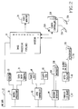
- FIG. 2 A block diagram of the video processor 25 which is housed in the cabinet 27 is illustrated in Figure 2.
- the various components of the system are interconnected by a VME bus 37.
- the processor includes a microcomputer 39, the data entry terminal 31 and the printer 33, a hard disk memory 41 and a floppy disk memory 43 and their controller 45, an encoder interface 44 which provides inputs from the optical encoders 35A and 35B, and a parallel input/output board 47 which also performs timing functions.
- the input/output board 47 interfaces with an optoisolator panel 49 which provides isolated signals from the optosensors 17a and 17b.
- the input/output board 47 also provides through the optoisolator panel 49 contact outputs for alarms generated by the system and signal for controlling a reject station (not shown) which diverts rejected panels downstream of the conveyor 9b.
- the video processor 25 also includes image processing pipelines 51. These image processing pipelines control the cameras 23a and 23b and receive video signals from these cameras through camera controllers 53a and 53b. As will be discussed, the image processing pipelines 51 process the raw video data for transmission over the VME bus 37 to the microprocessor 39. The image processing pipelines also supply video signals to the monitor 29.
- the image processing pipelines 51 are illustrated in block diagram form in Figure 3. These pipelines include a number of special purpose processors, all residing on the VME bus 37. In the exemplary system, the special purpose processors are all image processing boards manufactured by Data Cube, Inc. Each of the cameras 23a and 23b sweep the elements of the linear array at a rate of 1000 lines per second to generate analog electrical signals identified in Figure 3 as channel zero and channel 1 signals, respectively. These analog video signals are applied to line scan interface boards (MAX-SCAN) 55a and 55b which digitize the analog signals for storage in Capture ROI (region of interest) modules 57a and 57b. Each of the capture ROI boards 57a and 57b has a memory array which is 2000 by 4000 pixels with 8-bit resolution.
- MAX-SCAN line scan interface boards
- each of the Capture ROI boards 57a and 57b can store data for two separate panels. Thus, while data is being read out for a previously imaged panel, data can be read in for the next panel.
- the images captured by the two cameras are queued for transmission over a line 61 in RS-170 video format to a MAX-SIGMA board 63 which is configured as a Laplacian filter.
- the filtered output of the MAX-SIGMA board 63 is transmitted over the line 65 also in RS-170 video format to a FEATUREMAX board 67 which is a multilevel threshold detector.
- the FEATUREMAX board can compare the filtered gray-scale values to a number of positive and negative thresholds. Since the defects to be detected have a lower reflectivity than the unblemished portions of the panels, the negative thresholds are used.
- the FEATUREMAX board 67 generates a table of hits identifying the pixels having gray-scale values below the selected negative thresholds.
- the hit table records the x, y coordinates of the hit and includes for each hit two bits indicating the lowest threshold breached.
- the Laplacian filter function applied by the MAX SIGMA board 63 enhances the contrast of the gray-scale values of the captured image, and therefore enhances the definition of the edges of the defects.
- the thresholds applied by the FEATUREMAX board 67 are then selected to detect these edge features which reduces the number of hits and therefore the amount of data that must be processed.
- the table of hits generated by the FEATUREMAX board provides the basis upon which the acceptance/rejection decision is made by the microprocessor 39.
- a Display ROI board 69 selects among the raw gray scale data on lines 61 from a selected one of the Capture ROI boards 57a or 57b, or the filtered output of the MAX SIGMA board 63 on the lines 65 and sends the resulting image to a MAX-GRAPH board 71 over lines 73.
- the MAX-GRAPH board 71 can superimpose over the image received from the Display ROI the processed hit data received over the VME bus 37 from the digital processor 39. The composite image is then passed over lines 75 to the display monitor 29.
- a novel feature of the invention lies in the implementation of the threshold processing by the FEATURE-MAX board 67.
- the size and desired resolution of the image dictates that the images of the panels 5 require as many as approximately 2000 pixels in the cross web direction and approximately 1500 pixels in the down web direction for the largest panel which is 24 inches by 18 inches.
- the FEATUREMAX board 67 is limited to processing frames of 512 cross web pixels by 483 down web pixels. In order to process the entire panel image with the desired resolution, the FEATUREMAX board 67 is used to successively process a multiplicity of frames covering the panel 5.
- threshold processing is restricted to processing only pixels on the board. In the exemplary system, only pixels more than 0.25 inches from the edges of the panel are processed. This is not a drawback since generally components are not placed closer than one quarter inch from the edge of a printed circuit board in any event.
- the scheme for utilizing the FEATUREMAX board with a frame size of 512 by 483 pixels to inspect large panels is illustrated in Figure 4.
- the array 77 stored in the Capture ROI boards 59 is 2048 pixels wide and covers an area 26.6 inches in width W thereby providing a resolution of 0.013 inches at 77 pixels per inch.
- the array 77 is also 2048 pixels high representing a length L of 24.6 inches along the conveyor thereby providing a resolution of 0.012 inches for each pixel at 83.3 pixels per inch.
- the largest panels inspected are 24 inches by 21 inches as represented by the outline 79 superimposed on the capture ROI array 77.
- the smallest panel inspected by the exemplary system is 12 inches by 12 inches as represented by the outline 81 in Figure 4.
- the feeder system left justifies the panels as they are loaded onto the conveyor 9a so that they are all spaced a fixed distance from the left margin in the Capture ROI array 77.
- the optosensor and encoder are used to initiate capture of the data as described so that the data for all of the panels starts at a fixed distance from the top of the Capture ROI array.
- the number of pixels needed to cover the panel exceeds the frame size of the FEATUREMAX board.
- successive sections such as the sections 83, 85, 87 and 89, each equal in size to the 512 by 483 pixel frame size of the FEATUREMAX board are successively transferred to the FEATUREMAX board for processing.
- sections more than one quarter inch dimension B in Figure 4 from the edges of the panel image are transferred to the FEATUREMAX board.
- the successive sections each equal to a frame of the FEATUREMAX board, are transferred to the FEATUREMAX board until the entire panel has been processed.
- the frame When less than a full frame remains to be processed at the right and at the bottom, the frame is moved left or up to within one quarter inch of the right and/or the bottom respectively of the image, thus, overlapping a previously processed area as shown at the left side 91 of the section 85, the upper portion 93 of the section 87 and by the portions 95 and 97 of the section 89. Any resultant redundancy is eliminated as will be seen in the processing of the data. -Since the data is generally extremely sparse, this does not burden the processing.
- the digitized video data are entered into the Capture ROI boards 57a and 57b in real time as the panels move past the optical data acquisition system lines of sight. This data acquisition is effected independently for the two channels, channel zero and channel one, inspecting opposite sides of the panels at the inspection stations 3a and 3b, respectively.
- a flow chart for a suitable program implemented by the microprocessor 39 to process one channel for a panel is illustrated in Figure 5.
- the panel is allocated a descriptor at 101 for identification.
- the timer in the input/output timer board 47 is then set for the first speed measurement and the count generated by the encoder 35a or 35b is cleared all as indicated at 103.
- the encoder is read and used to calculate the speed of the panel on the conveyor as indicated at 105.
- the timer is then set for the calculated time at which the panel will reach the camera line of sight as indicated at 107.
- a signal is sent to MAX-SCAN, 55a or 55b, to initiate image capture as indicated at 109.
- the capture ROI board for the channel 57a or 57b generates an interrupt when the image capture has been completed. Upon receiving this interrupt at 111, the captured image is made available for processing by placing it in a queue at 113.
- one FEATUREMAX board processes the images generated by both of the channels. When FEATUREMAX is available, FEATUREMAX processing of the image is initiated at 115. As discussed, the FEATUREMAX board generates an array of hit tables indicating the number of pixels having gray-scale values which are below selected thresholds, the addresses of those pixels and the lowest threshold breached.
- the hit descriptor identifying the array of tables of hits for the processed image is queued for processing at 117.
- the results of this processing of the hits is received at 119 and the final output for the channel is set at 121. For instance, if the indication received from the processing subsystem is that the panel is to be rejected, the output is set to cause the panel to be diverted downstream.
- This completion of processing of the channel is indicated 123 and the program waits at 125 for another panel to approach the inspection station.
- the state flag is set to start at 139, so that when the state is checked at 141, the program will set the pixel index to the initial index of the frame at 143, and set the thresholds at 145.
- the FEATUREMAX board is provided with four thresholds against which it compares the gray scale value for each pixel in the frame being processed. With the thresholds set, the input channel to be processed is set at 147 and the FEATUREMAX board is started at 149. The FEATUREMAX board then compares the gray scale value for each of the pixels in the frame to the four thresholds and stores the hits, that is the pixels having a gray-scale value below any of the thresholds, in a hit table.
- the state flag is then set to MIDDLE at 151 and the program waits for the next interrupt.
- the pixel index is then set to the initial pixel of the next frame at 153 and the next frame is processed by FEATUREMAX at 155. While this is occurring, the hit count for the previous frame and the hits for the previous frame are transmitted to the microprocessor at 157 and 159, respectively. If there are more frames to be processed as determined at 161, the state remains MIDDLE and the additional frames are processed in a similar manner.
- the state is set to END at 163. Following the next Capture ROI interrupt FEATUREMAX operation is terminated at 165.
- the hit count for the last board is transmitted at 167 and the hits for the last frame are transmitted at 169 before the state is set to DONE at 171.
- FIG. 7 The flow chart for a routine for unloading hits from the FEATUREMAX board to the microprocessor as called for at 109 and 169 in the flow chart of Figure 6 is illustrated in Figure 7.
- This unloading of the x and y coordinates of the hits and the thresholds breached must be implemented very rapidly and is accomplished during the vertical blanking interval of the Capture ROI board from which the data is being processed.
- a POINTER is set to the location in the memory of the microprocessor at which storing of the hit table is to be initiated, and a parameter TOTAL, which tracks the number of hits transferred to computer memory, is initialized to zero.
- a loop is then entered at 175 to transmit the hit table, with the number of hits to be transferred equal to the count generated by the FEATUREMAX board of the number of hits recorded in the hit table for the frame being processed. Until that total number of hits has been transmitted, an entry from the hit table is fetched at 177.
- the microprocessor in defining the frame sized sections of the Capture ROI to be successively processed by the FEATUREMAX board specifies minimum x and y coordinates of the frame to eliminate the overlap.
- the data for the hit is copied to the computer memory at 183.
- the parameter TOTAL and the POINTER are then incremented at 185.
- the video active, VA, bit generated by the Capture ROI board is then checked at 187. If this video active bit indicates that the Capture ROI board is still in the vertical blanking interval, than COUNTER is decremented at 191 and the additional entries in the hit table are transmitted to microprocessor memory in a similar manner.
- a parameter ACTUAL indicating the number of hits actually transferred to the microcomputer is set equal to total at 193. If a RESTART flag indicating that there are additional frames of the Capture ROI image to be processed is set, as determined at 195, then a START NEW FRAME flag is set at 197 before the routine returns to the calling program at 199.
- FIG. 8 A flow chart for image and hit table processing by the microprocessor 39 is illustrated in Figure 8. With the system in the inspection mode as indicated 201, if a break key is depressed as determined at 203, indicating that the operator is interfacing with the system, the inspection mode is exited at 205 for the menu mode. If the operator is not interfacing with the system, a determination is made at 207 if an image is available for processing. When an image is available, the edge of the panel within the image is located at 209. This location of the panel edge is then used to plot the expected board outline on the MAX-GRAPH board 71, which it will be recalled, is used to geneiate the display on the monitor 29.
- the measured board outline can also be plotted on MAX-GRAPH as indicated at 215.
- This measured board outline is established by routine which locates the edges of the board from the gray-scale values of the image stored in Capture ROI.
- the total number of hits for the panel is determined at 219. This count is the count of the number of pixels for which the gray-scale value exceeded any of the four thresholds. If this total hit count exceeds a preselected value, as determined at 221, the panel is rejected. Otherwise, proximate hits are associated into blobs and the number of hits in each blob is calculated as determined at 223. The size of the largest blob is then determined at 225 and if this largest blob size exceeds a threshold, the reject flag is set at 229. The hits are then plotted on the MAX-GRAPH superimposed on the outline of the panel as indicated at 231. The memory is then released at 233 for receiving new hit table data from the FEATUREMAX as indicated at 233 and the results are logged on the printer at 235. This loop is repeated as long as the microprocessor remains in the inspection mode.
- FIG. 9a and 9b The flow chart for the routine for associating proximate hits into blobs and calculating the number of hits in each blob is illustrated in Figure 9a and 9b. Data structures used by this routine are illustrated in Figures 10 through 12.
- Figure 10 illustrates the hit array 237 in which the hits are sequentially numbered and their x and y coordinates are stored. Up to a maximum number of hits can be stored in the array. This max number of hits corresponds to the maximum number of pixels exceeding a threshold that can be tolerated.
- the blob tag array 239 of Figure 11 indicates the identification of a blob, if any, with which each of the numbered hits has been associated.
- the blob array 241 shown in Figure 12 lists for each identified blob the number of hits associated with the blob and the identification of "which" hits are associated with the blob.
- the "which" entry 243 has been expanded in Figure 12 to show that it can include the identification of a number of hits up to a maximum size for the blob. If any panel has a blob with the maximum number of hits in it, the panel is rejected.
- a parameter INDEX which points to a hit of interest is initialized to two at 245. This starts the processing with the second set of x, y coordinates in the hit array. Another pointer identified as POINTER is set to one less than INDEX as indicated at 247. Next, the distance D y from the y value of the hit pointed to by INDEX to the y value of the hit pointed to by POINTER is calculated in 249. If this distance, D y is not greater than a maximum allowable distance between hits associated into a blob, D spacigg as determined at 251, then the absolute value of the distance, D x for the same two hits is calculated at 253.
- D X is less than or equal to D spacing as determined at 255, then a flag CONNECTED is set to true at 257 indicating that the hits pointed to by INDEX and POINTER are close enough to be associated in a blob. If the x spacing is too great to associate the hits into a blob, POINTER is decremented at 259 to move backward through the hit table and the proximity test is repeated until the hit of interest has been evaluated with respect to all of the earlier hits in the hit table as determined at 261.
- the blob tag for the blob with which the hit is associated is entered at 265 in the blob tag array.
- the "how many" value for that blob in the blob array is then incremented at 267, and the hit indicated by INDEX is entered into the "which" array at the position pointed at by "how many” as indicated at 269.
- the pointer INDEX is then incremented by one at 271.
- a new blob is indicated at 273 in the blob tag table for the hit pointed to by INDEX and the cooresponding "how many" entry in the blob array is initialized to one at 275.
- the hit pointed to by INDEX is then copied into the "which" array at the first position for the new blob as indicated at 277.
- NEW BLOB is then incremented by one at 279 for the next blob and INDEX is incremented at 271 to select the next hit in the hit array. If all of the hits in the hit table has not yet been evaluated as determined at 281, the program loops back to 247, otherwise the routine is exited at 283.
- the vision systems of the embodiments described and illustrated above have enabled vision processing equipment with limited area coverage to be used to inspect panels of larger area. Furthermore, the data indicative of selected defects can be reduced to reduce processing time as well as the capacity required for the vision systems to perform the inspection on line.
Applications Claiming Priority (2)
| Application Number | Priority Date | Filing Date | Title |
|---|---|---|---|
| US07/549,570 US5325443A (en) | 1990-07-06 | 1990-07-06 | Vision system for inspecting a part having a substantially flat reflective surface |
| US549570 | 1990-07-06 |
Publications (2)
| Publication Number | Publication Date |
|---|---|
| EP0465233A2 true EP0465233A2 (de) | 1992-01-08 |
| EP0465233A3 EP0465233A3 (en) | 1992-11-25 |
Family
ID=24193542
Family Applications (1)
| Application Number | Title | Priority Date | Filing Date |
|---|---|---|---|
| EP19910306023 Withdrawn EP0465233A3 (en) | 1990-07-06 | 1991-07-02 | Vision inspection systems |
Country Status (3)
| Country | Link |
|---|---|
| US (1) | US5325443A (de) |
| EP (1) | EP0465233A3 (de) |
| JP (1) | JP3041090B2 (de) |
Cited By (6)
| Publication number | Priority date | Publication date | Assignee | Title |
|---|---|---|---|---|
| EP0571728A2 (de) * | 1992-05-27 | 1993-12-01 | WindmÀ¶ller & Hölscher | Verfahren zur Prüfung der Ausbildung kontinuierlich geförderter Werkstücke |
| GB2270227A (en) * | 1992-08-28 | 1994-03-02 | Surface Inspection Ltd | Linescan visual monitoring system |
| EP0803903A2 (de) * | 1996-04-25 | 1997-10-29 | Nec Corporation | Automatisches, visuelles Inspektions- und Fehlerkategorisier-Gerät |
| WO1998008080A1 (de) * | 1996-08-20 | 1998-02-26 | Zellweger Luwa Ag | Verfahren und vorrichtung zur erkennung von fehlern in textilen flächengebilden |
| WO2000028309A1 (en) * | 1998-11-05 | 2000-05-18 | Samsung Electronics Co., Ltd. | Method for inspecting inferiority in shape |
| WO2005058717A1 (en) * | 2003-12-19 | 2005-06-30 | Chep Australia Limited | Software and methods for automated pallet inspection and repair |
Families Citing this family (23)
| Publication number | Priority date | Publication date | Assignee | Title |
|---|---|---|---|---|
| US5586058A (en) * | 1990-12-04 | 1996-12-17 | Orbot Instruments Ltd. | Apparatus and method for inspection of a patterned object by comparison thereof to a reference |
| JP2585594Y2 (ja) * | 1993-03-10 | 1998-11-18 | 株式会社イナックス | 表面凹凸検査システム |
| JP3078685B2 (ja) * | 1993-08-06 | 2000-08-21 | 松下電器産業株式会社 | 位置認識方法 |
| US6181837B1 (en) | 1994-11-18 | 2001-01-30 | The Chase Manhattan Bank, N.A. | Electronic check image storage and retrieval system |
| JP2985160B2 (ja) * | 1995-03-01 | 1999-11-29 | 三菱電線工業株式会社 | Oリング検査装置 |
| JPH08313223A (ja) * | 1995-05-16 | 1996-11-29 | Ls Electro Galvanizing Co | 移動ストリップを監視する方法と装置 |
| US5913105A (en) * | 1995-11-29 | 1999-06-15 | Advanced Micro Devices Inc | Method and system for recognizing scratch patterns on semiconductor wafers |
| US5768443A (en) * | 1995-12-19 | 1998-06-16 | Cognex Corporation | Method for coordinating multiple fields of view in multi-camera |
| US5970166A (en) * | 1996-09-24 | 1999-10-19 | Cognex Corporation | System or method for identifying contents of a semi-opaque envelope |
| US5987159A (en) * | 1996-09-24 | 1999-11-16 | Cognex Corporation | System or method for detecting defect within a semi-opaque enclosure |
| US5949905A (en) * | 1996-10-23 | 1999-09-07 | Nichani; Sanjay | Model-based adaptive segmentation |
| US5757473A (en) * | 1996-11-13 | 1998-05-26 | Noranda, Inc. | Optical strain sensor for the measurement of microdeformations of surfaces |
| US5912984A (en) * | 1996-12-19 | 1999-06-15 | Cognex Corporation | Method and apparatus for in-line solder paste inspection |
| US6175415B1 (en) | 1997-02-19 | 2001-01-16 | United Technologies Corporation | Optical profile sensor |
| US6154561A (en) * | 1997-04-07 | 2000-11-28 | Photon Dynamics, Inc. | Method and apparatus for detecting Mura defects |
| US5905572A (en) * | 1997-08-21 | 1999-05-18 | Li; Ming-Chiang | Sample inspection using interference and/or correlation of scattered superbroad radiation |
| US6204469B1 (en) | 1999-03-04 | 2001-03-20 | Honda Giken Kogyo Kabushiki Kaisha | Laser welding system |
| JP4401590B2 (ja) * | 2000-06-19 | 2010-01-20 | キヤノン株式会社 | 画像データ処理方法及び画像データ処理装置 |
| US6735745B2 (en) * | 2002-02-07 | 2004-05-11 | Applied Materials, Inc. | Method and system for detecting defects |
| JP4562126B2 (ja) * | 2004-09-29 | 2010-10-13 | 大日本スクリーン製造株式会社 | 欠陥検出装置および欠陥検出方法 |
| US7751612B2 (en) | 2006-10-10 | 2010-07-06 | Usnr/Kockums Cancar Company | Occlusionless scanner for workpieces |
| US20110019243A1 (en) * | 2009-07-21 | 2011-01-27 | Constant Jr Henry J | Stereoscopic form reader |
| CN102841104A (zh) * | 2012-08-03 | 2012-12-26 | 杭州良淋电子科技有限公司 | 线材自动检验装置 |
Citations (3)
| Publication number | Priority date | Publication date | Assignee | Title |
|---|---|---|---|---|
| EP0095517A1 (de) * | 1982-05-28 | 1983-12-07 | Ibm Deutschland Gmbh | Verfahren und Einrichtung zur automatischen optischen Inspektion |
| EP0228963A2 (de) * | 1985-12-27 | 1987-07-15 | AT&T Corp. | Untersuchungssystem durch Linienabtastung für Schaltungsplatten |
| EP0460431A1 (de) * | 1990-06-07 | 1991-12-11 | Rautaruukki Oy | Verfahren und Apparat zur optischen Inspektion von band- oder blattförmigen Produkten |
Family Cites Families (11)
| Publication number | Priority date | Publication date | Assignee | Title |
|---|---|---|---|---|
| GB1430420A (en) * | 1972-04-24 | 1976-03-31 | Niemi A | Method and apparatus for analyzing a visible object |
| US4395698A (en) * | 1980-08-15 | 1983-07-26 | Environmental Research Institute Of Michigan | Neighborhood transformation logic circuitry for an image analyzer system |
| US4519041A (en) * | 1982-05-03 | 1985-05-21 | Honeywell Inc. | Real time automated inspection |
| US4500202A (en) * | 1982-05-24 | 1985-02-19 | Itek Corporation | Printed circuit board defect detection of detecting maximum line width violations |
| US4561104A (en) * | 1984-01-16 | 1985-12-24 | Honeywell Inc. | Automated inspection of hot steel slabs |
| US4733229A (en) * | 1984-01-24 | 1988-03-22 | Whitehead Frank R | Highlighting gray scale video display terminal |
| US4811410A (en) * | 1986-12-08 | 1989-03-07 | American Telephone And Telegraph Company | Linescan inspection system for circuit boards |
| US4972494A (en) * | 1988-02-26 | 1990-11-20 | R. J. Reynolds Tobacco Company | Package inspection system |
| US4868651A (en) * | 1988-05-17 | 1989-09-19 | S&S Inficon, Inc. | Digital radiography with image brightness and contrast normalization |
| US4929845A (en) * | 1989-02-27 | 1990-05-29 | At&T Bell Laboratories | Method and apparatus for inspection of substrates |
| US4963036A (en) * | 1989-03-22 | 1990-10-16 | Westinghouse Electric Corp. | Vision system with adjustment for variations in imaged surface reflectivity |
-
1990
- 1990-07-06 US US07/549,570 patent/US5325443A/en not_active Expired - Fee Related
-
1991
- 1991-07-02 EP EP19910306023 patent/EP0465233A3/en not_active Withdrawn
- 1991-07-05 JP JP3190812A patent/JP3041090B2/ja not_active Expired - Lifetime
Patent Citations (3)
| Publication number | Priority date | Publication date | Assignee | Title |
|---|---|---|---|---|
| EP0095517A1 (de) * | 1982-05-28 | 1983-12-07 | Ibm Deutschland Gmbh | Verfahren und Einrichtung zur automatischen optischen Inspektion |
| EP0228963A2 (de) * | 1985-12-27 | 1987-07-15 | AT&T Corp. | Untersuchungssystem durch Linienabtastung für Schaltungsplatten |
| EP0460431A1 (de) * | 1990-06-07 | 1991-12-11 | Rautaruukki Oy | Verfahren und Apparat zur optischen Inspektion von band- oder blattförmigen Produkten |
Cited By (13)
| Publication number | Priority date | Publication date | Assignee | Title |
|---|---|---|---|---|
| DE4217623B4 (de) * | 1992-05-27 | 2008-02-07 | Windmöller & Hölscher Kg | Verfahren zur Prüfung der Ausbildung kontinuierlich geförderter Werkstücke |
| EP0571728A3 (en) * | 1992-05-27 | 1995-09-06 | Windmoeller & Hoelscher | Method for checking the formation of continuously advanced products |
| EP0571728A2 (de) * | 1992-05-27 | 1993-12-01 | WindmÀ¶ller & Hölscher | Verfahren zur Prüfung der Ausbildung kontinuierlich geförderter Werkstücke |
| GB2270227A (en) * | 1992-08-28 | 1994-03-02 | Surface Inspection Ltd | Linescan visual monitoring system |
| EP0803903A2 (de) * | 1996-04-25 | 1997-10-29 | Nec Corporation | Automatisches, visuelles Inspektions- und Fehlerkategorisier-Gerät |
| EP0803903A3 (de) * | 1996-04-25 | 1998-11-25 | Nec Corporation | Automatisches, visuelles Inspektions- und Fehlerkategorisier-Gerät |
| WO1998008080A1 (de) * | 1996-08-20 | 1998-02-26 | Zellweger Luwa Ag | Verfahren und vorrichtung zur erkennung von fehlern in textilen flächengebilden |
| WO2000028309A1 (en) * | 1998-11-05 | 2000-05-18 | Samsung Electronics Co., Ltd. | Method for inspecting inferiority in shape |
| US6895108B2 (en) | 1998-11-05 | 2005-05-17 | Samsung Electronics Co., Ltd. | Method for inspecting defects in the shape of object |
| WO2005058717A1 (en) * | 2003-12-19 | 2005-06-30 | Chep Australia Limited | Software and methods for automated pallet inspection and repair |
| US7958624B2 (en) | 2003-12-19 | 2011-06-14 | Chep Technology Pty Limited | Software and methods for automated pallet inspection and repair |
| US8881360B2 (en) | 2003-12-19 | 2014-11-11 | Chep Technology Pty Limited | Software and methods for automated pallet inspection and repair |
| US10092987B2 (en) | 2003-12-19 | 2018-10-09 | Chep Technology Pty Limited | Software and methods for automated pallet inspection and repair |
Also Published As
| Publication number | Publication date |
|---|---|
| US5325443A (en) | 1994-06-28 |
| EP0465233A3 (en) | 1992-11-25 |
| JP3041090B2 (ja) | 2000-05-15 |
| JPH04270950A (ja) | 1992-09-28 |
Similar Documents
| Publication | Publication Date | Title |
|---|---|---|
| US5325443A (en) | Vision system for inspecting a part having a substantially flat reflective surface | |
| US4692943A (en) | Method of and system for opto-electronic inspection of a two-dimensional pattern on an object | |
| US4446481A (en) | Automatic product inspection system | |
| EP0089212B1 (de) | Verfahren und Vorrichtung zum Sortieren von Gegenständen | |
| EP0483966B1 (de) | Verfahren und Vorrichtung zur Untersuchung eines transparenten oder durchscheinenden Gegenstandes wie beispielsweise einer Flasche | |
| EP0597639B1 (de) | Berührungslose Erkennung von Oberflächenfehlern | |
| CN110296997B (zh) | 基于机器视觉的陶瓷瓦的缺陷检测方法及装置 | |
| US20040201669A1 (en) | Web inspection system | |
| CA1179426A (en) | Method and apparatus for inspecting engine head valve retainer assemblies for missing keys | |
| KR880002322B1 (ko) | 이동중인 스크립상의 표면결함 감지방법 및 장치 | |
| US4678920A (en) | Machine vision method and apparatus | |
| KR960003873B1 (ko) | 결함표시 방법 및 장치 | |
| US3729619A (en) | Apparatus for surface inspection of moving material with defect type recognition | |
| KR100415796B1 (ko) | 스캐닝간격결정방법 | |
| JPH08261737A (ja) | 網形状物検査装置及び網形状物検査方法 | |
| CN112240888A (zh) | 一种视觉检测方法及视觉检测系统 | |
| JPH10137696A (ja) | 選別方法及びその装置 | |
| JPH08297020A (ja) | 欠陥検査方法とその装置 | |
| JPH09178444A (ja) | 画像処理による形状測定方法とその選別装置 | |
| JPS63288593A (ja) | 搬送物体撮影装置 | |
| JPH0792106A (ja) | 表面欠陥検査装置 | |
| JP3412732B2 (ja) | 欠陥検査方法及びその装置 | |
| JPH0829357A (ja) | 自動化ライン外観検査装置 | |
| JPH0554127A (ja) | 視覚認識装置 | |
| CN114798474A (zh) | 一种基于机器视觉的电容器引脚距离测量及分拣方法 |
Legal Events
| Date | Code | Title | Description |
|---|---|---|---|
| PUAI | Public reference made under article 153(3) epc to a published international application that has entered the european phase |
Free format text: ORIGINAL CODE: 0009012 |
|
| AK | Designated contracting states |
Kind code of ref document: A2 Designated state(s): DE FR GB IT |
|
| PUAL | Search report despatched |
Free format text: ORIGINAL CODE: 0009013 |
|
| AK | Designated contracting states |
Kind code of ref document: A3 Designated state(s): DE FR GB IT |
|
| 17P | Request for examination filed |
Effective date: 19930521 |
|
| STAA | Information on the status of an ep patent application or granted ep patent |
Free format text: STATUS: THE APPLICATION HAS BEEN WITHDRAWN |
|
| 18W | Application withdrawn |
Withdrawal date: 19961009 |