EP0465002B1 - Programmierbare Schaltung zur Leistungsverminderung in einer programmierbaren logischen Schaltung - Google Patents
Programmierbare Schaltung zur Leistungsverminderung in einer programmierbaren logischen Schaltung Download PDFInfo
- Publication number
- EP0465002B1 EP0465002B1 EP91304675A EP91304675A EP0465002B1 EP 0465002 B1 EP0465002 B1 EP 0465002B1 EP 91304675 A EP91304675 A EP 91304675A EP 91304675 A EP91304675 A EP 91304675A EP 0465002 B1 EP0465002 B1 EP 0465002B1
- Authority
- EP
- European Patent Office
- Prior art keywords
- input
- programming
- buffer
- data
- storage element
- Prior art date
- Legal status (The legal status is an assumption and is not a legal conclusion. Google has not performed a legal analysis and makes no representation as to the accuracy of the status listed.)
- Expired - Lifetime
Links
- 239000000872 buffer Substances 0.000 claims description 55
- 230000000295 complement effect Effects 0.000 claims description 19
- 230000006870 function Effects 0.000 claims description 19
- 238000000034 method Methods 0.000 claims description 7
- 238000010586 diagram Methods 0.000 description 6
- 230000002411 adverse Effects 0.000 description 2
- 230000000694 effects Effects 0.000 description 2
- 238000003491 array Methods 0.000 description 1
Images
Classifications
-
- H—ELECTRICITY
- H03—ELECTRONIC CIRCUITRY
- H03K—PULSE TECHNIQUE
- H03K19/00—Logic circuits, i.e. having at least two inputs acting on one output; Inverting circuits
- H03K19/02—Logic circuits, i.e. having at least two inputs acting on one output; Inverting circuits using specified components
- H03K19/173—Logic circuits, i.e. having at least two inputs acting on one output; Inverting circuits using specified components using elementary logic circuits as components
- H03K19/177—Logic circuits, i.e. having at least two inputs acting on one output; Inverting circuits using specified components using elementary logic circuits as components arranged in matrix form
- H03K19/17748—Structural details of configuration resources
-
- H—ELECTRICITY
- H03—ELECTRONIC CIRCUITRY
- H03K—PULSE TECHNIQUE
- H03K19/00—Logic circuits, i.e. having at least two inputs acting on one output; Inverting circuits
-
- H—ELECTRICITY
- H03—ELECTRONIC CIRCUITRY
- H03K—PULSE TECHNIQUE
- H03K19/00—Logic circuits, i.e. having at least two inputs acting on one output; Inverting circuits
- H03K19/0008—Arrangements for reducing power consumption
- H03K19/0016—Arrangements for reducing power consumption by using a control or a clock signal, e.g. in order to apply power supply
-
- H—ELECTRICITY
- H03—ELECTRONIC CIRCUITRY
- H03K—PULSE TECHNIQUE
- H03K19/00—Logic circuits, i.e. having at least two inputs acting on one output; Inverting circuits
- H03K19/02—Logic circuits, i.e. having at least two inputs acting on one output; Inverting circuits using specified components
- H03K19/173—Logic circuits, i.e. having at least two inputs acting on one output; Inverting circuits using specified components using elementary logic circuits as components
- H03K19/177—Logic circuits, i.e. having at least two inputs acting on one output; Inverting circuits using specified components using elementary logic circuits as components arranged in matrix form
- H03K19/17704—Logic circuits, i.e. having at least two inputs acting on one output; Inverting circuits using specified components using elementary logic circuits as components arranged in matrix form the logic functions being realised by the interconnection of rows and columns
-
- H—ELECTRICITY
- H03—ELECTRONIC CIRCUITRY
- H03K—PULSE TECHNIQUE
- H03K19/00—Logic circuits, i.e. having at least two inputs acting on one output; Inverting circuits
- H03K19/02—Logic circuits, i.e. having at least two inputs acting on one output; Inverting circuits using specified components
- H03K19/173—Logic circuits, i.e. having at least two inputs acting on one output; Inverting circuits using specified components using elementary logic circuits as components
- H03K19/177—Logic circuits, i.e. having at least two inputs acting on one output; Inverting circuits using specified components using elementary logic circuits as components arranged in matrix form
- H03K19/17748—Structural details of configuration resources
- H03K19/1776—Structural details of configuration resources for memories
-
- H—ELECTRICITY
- H03—ELECTRONIC CIRCUITRY
- H03K—PULSE TECHNIQUE
- H03K19/00—Logic circuits, i.e. having at least two inputs acting on one output; Inverting circuits
- H03K19/02—Logic circuits, i.e. having at least two inputs acting on one output; Inverting circuits using specified components
- H03K19/173—Logic circuits, i.e. having at least two inputs acting on one output; Inverting circuits using specified components using elementary logic circuits as components
- H03K19/177—Logic circuits, i.e. having at least two inputs acting on one output; Inverting circuits using specified components using elementary logic circuits as components arranged in matrix form
- H03K19/1778—Structural details for adapting physical parameters
- H03K19/17784—Structural details for adapting physical parameters for supply voltage
Definitions
- the present invention relates generally to integrated circuit devices and more specifically to programmable logic devices which are configurable by a user.
- Programmable logic devices are becoming increasingly popular in the electronics industry because of their flexibility. These devices allow a user to configure a standard part to perform a wide variety of standard logic functions. Since a single standard device can be configured many different ways, the total cost of using such a device in a system can be significantly less than the cost of custom design parts, especially when the product volume is not large. If changes or update are needed to the programmed logic function, some types of devices can be reprogrammed.
- a logic function for a programmable logic device will not utilize all the input lines of the programmable logic device. These unutilized input lines are termed "don't care” inputs because they do not have an effect in the logic functions programmed in the programmable logic device.
- the components which define a logic device as well as the device itself consume power during operations of the device.
- the problem with the unutilized or "don't care" inputs is that the components corresponding to those inputs consume power during normal operation of the device, even though the inputs are not used in the programmed logic function. Consequently, the actual power needed by the programmable logic device to perform its logic function is unnecessarily increased by the components of the unutilized inputs.
- US-A-4763020 discloses a programmable logic array with a plurality of pairs of input lines. One of the lines of each pair carries a non-inverted signal whilst the other line of each pair carries an inverted signal. If a pair of input lines is connected to a non-used input, the pair of input lines is set to a low level.
- programming information corresponding to an input signal is loaded into a shift register. This input information is compared with programming information corresponding to a second, complementary input signal to determine if the two signals are used by the programmable logic device. If the two inputs are not used, a bit is stored in a memory cell indicating such nonuse. An input buffer is disabled when the bit in the memory cell indicates the complementary signals corresponding to that input buffer are not used.
- a programmable logic device comprising:
- a circuit block for a programmable logic device comprising:
- a method for determining whether an input to a programmable logic device will be used in a logic function comprising the steps of:
- the memory cell 28 should be an EPROM or EEPROM component as well.
- the AND/OR array 10 is an SRAM based device, the memory cell 28 should be SRAM also.
- the SRAM memory cell can have a battery back-up, so that when the device is turned off the data stored in the memory cell 10 will be saved.
- Co-pending application EP 90 314 143.0 describes the design and operation of a preferred design for an SRAM based programmable logic device.
- the invention is described in terms of an automatic method for determining whether an input signal is used, and then enabling or disabling an input buffer based on the use or non-use of its corresponding signal line.
- the enable/disable information could be programmed directly into the memory cell 28 when programming the programmable logic device 11 .
- the invention is not limited to use with logic devices containing AND/OR arrays. This invention could be used with other types of logic devices.
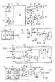
- FIG. 1 a portion of a programmable logic device 11 is shown.
- Input pads 24 , 26 are connected to input buffer 20 , 22 respectively.
- Each input buffer 20 , 22 provides a true signal line 14 , 18 and a complement signal line 12 , 16 . Only two input pads 24 , 26 and input buffers 20 , 22 are shown in Figure 1, but an actual device typically has a much larger number.
- Each of the signal lines 12-18 is connected to an AND/OR array 10 .
- a user can configure the AND/OR array 10 to perform a particular logic function. When programmed, it is common to have input signal lines which are not utilized in the logic function.
- memory cells 28 , 30 are used to store a bit indicating use or nonuse of a signal line 14 , 18 and its complement 12 , 16 . If a signal line 14 , 18 and its complement 12 , 16 will be used, the bit in the memory cell 28 , 30 will enable the input buffer 20 , 22 . If however, the signal line 14 , 18 and its complement 12 , 16 will not be used in the logic function, the input buffer 20 , 22 that corresponds to the unused lines will be disabled.
- Output signal lines 32 , 34 from the AND/OR array 10 are connected to output logic macrocells 36 , 38 .
- Output buffers 40 , 42 are connected between the output logic macrocells 36 , 38 and the output pads 44 , 46 .
- signal lines 48 , 50 are connected to the output logic macrocells 36 , 38 .
- input buffers 52 , 54 are connected to the output logic macrocells 36 , 38 and generate signal lines 62 , 66 and complements 60 , 64 respectively.
- Memory cells 56 , 58 store a bit which can enable or disable the input buffers 52 , 54 based on the signal lines used in by programmed logic function.
- FIG. 2 illustrates one implementation of the input buffer 20 .
- a NAND gate 70 is connected to the memory cell 28 and input pad 24 .
- a bit MATCH 74 is generated and stored in the memory cell 28 .
- the signal DISABLE is preferably taken from the complement output of cell 28 , so that DISABLE is complementary to MATCH.
- the signal DISABLE 68 is set low thereby keeping the output of the NAND gate 70 high.
- An inverter 72 is connected to the NAND gate 70 , and the output of the inverter 72 is signal line 14 .
- an inverter 76 is connected to inverter 72 , and a signal is generated on line 12 is generated.
- Figure 3 shows an alternative input buffer 52 which can be used when either an input signal line 24 or a feedback line 110 is needed.
- Input line, or pad, 24 is connected to NAND gate 112 , which in turn is connected to NAND gate 114 .
- the DISABLE signal from storage element 28 is connected to NOR gates 116 , 118 .
- a signal FB Enable is connected to NOR gate 116 and inverter 120 , which is in turn connected to NOR gate 118 .
- the feedback signal on line 110 is connected to NAND gate 122 , as is the output of NOR gate 118 .
- NOR gate 116 is connected to NAND gate 112
- NAND gate 122 is connected to NAND gate 114 .
- DISABLE has the same value as MATCH. If DISABLE is high, both NOR gate outputs are held low, holding NAND gates 112 and 122 low, and the output of NAND gate 114 high. If DISABLE is high, either the signal on pad 24 or the FB signal is connected to the output of gate 114 , depending on the value of FB Enable. Thus, DISABLE disables both input signals, or neither, depending on its value.
- Figure 4 depicts a simple block diagram of circuitry used for determining whether signal lines are used by the programmed logic function.
- Programming data is shifted into the serial shift register 82 as known in the art.
- a copy of the data is stored in the random access memory 84 while the data is programmed into the AND/OR array 10 .
- a second group of programming data is loaded into the shift register 82 .
- the addresses of the two groups of programming data are compared to insure the two groups are complementary. Addressing of the programming data is known in the art. If the two groups are complements of each other, the comparison circuitry 86 compares each element of the first group of programming data with corresponding elements in the second group of programming data.
- the bit MATCH 74 is set.
- the second group of programming data is then programmed into the AND/OR array 10 .
- the value of MATCH is programmed into the enable/disable bit for the input buffer corresponding to the first and second groups at the time the second group is programmed into the array 10 .
- Figure 5 illustrates the shift register 82 , the random access memory 84 , and the comparison circuitry 86 in greater detail. Only two elements 88, 90 in the shift register and two elements 92, 94 in the random access memory are shown in Figure 5 , but an actual device typically has a much larger number.
- Exclusive NOR gates 96, 98 in the comparison circuitry 86 are connected to elements 88, 90 in the shift register 82 and elements 92, 94 in the random access memory 84 . If elements 88, 90 have the same values as elements 92, 94 respectively, the output 100, 102 of the exclusive NOR gates 96, 98 will be high. Outputs 100, 102 are connected to AND gate 104 . When outputs 100, 102 are both high, indicating elements 88, 90 and elements 92 , 94 match, the output of AND gate 104 is high. AND gate 106 is connected to AND gate 104 and an address comparator 108 .
- the signal MATCH 74 is generated indicating the two groups of programming data are not used in the programmed logic function.
- MATCH is inverted to generate the signal MATCH of Figures 2 and 3 , and, is connected to the memory cell 28 corresponding to the input addressed by the groups of programming data currently found in the shift register 82 and the memory 84 .
- the output 100, 102 of one or more of the exclusive NOR gates 96, 98 will be low. In this case, the signal MATCH 74
Landscapes
- Physics & Mathematics (AREA)
- Mathematical Physics (AREA)
- Engineering & Computer Science (AREA)
- Computer Hardware Design (AREA)
- Computing Systems (AREA)
- General Engineering & Computer Science (AREA)
- Logic Circuits (AREA)
Claims (18)
- Progammierbares Logikbauelement (11), das folgendes aufweist:eine Anzahl von Eingängen (24, 26);eine Logikanordnung bzw. ein Logikbaustein (10), die bzw. der mit den Eingängen (24, 26) verbunden ist, um eine ihrer bzw. seiner Logikfunktionen festzulegen;eine Speichereinrichtung (28, 30), die mit jedem Eingang (24, 26) verbunden ist, um eine Konfigurationsinformation zum selektiven Sperren bzw. Deaktivieren seiner zugehörigen Eingänge (24, 26) zu speichern;eine Anzahl von Ausgängen (44, 46), die mit der Anordnung bzw. dem Baustein verbunden sind, dadurch gekennzeichnet, daß folgendes vorgesehen ist:ein Programmierpuffer (82) zum Halten von Programmierdaten. um einen Abschnitt des Bauelements zu programmieren;eine Anzahl von Speichervorrichtungen (84), die mit dem Programmierpuffer (82) zum Speichern einer Kopie der Programmierdaten verbunden sind, die zuvor von dem Programmierpuffer (82) gehalten wurden;eine Vergleichsschaltung (86), die mit dem Programmierpuffer (82) und der Speichervorrichtung (84) zum Erzeugen eines Vergleichssignals verbunden ist, das eine Übereinstimmung zwischen Daten in dem Programmierpuffer (82) und Daten in der Anzahl von Speichervorrichtungen (84) anzeigt; undeine Einrichtung zum Speichern von Konfigurationsinformation in den Speichereinrichtungen (28, 30), und zwar basierend auf dem Vergleichssignal.
- Bauelement nach Anspruch 1, bei welchem jede Speichereinrichtung eine Speichervorrichtung (28, 30) aufweist, in die während der Programmierung des Bauelements geschrieben werden kann.
- Bauelement nach Anspruch 1 oder 2, bei welchem jede Speichereinrichtung (28, 30) ein SRAM aufweist.
- Bauelement nach Anspruch 1 oder 2, bei welchem jede Speichereinrichtung eine programmierbare Nur-Lese-Speichereinrichtung (28, 30) aufweist.
- Bauelement nach irgendeinem der Ansprüche 1 bis 4, bei welchem jeder Eingang mit der Anordnung bzw. dem Baustein (10) über einen Eingangspuffer (20; 52) verbunden ist, und bei welchem die zugeordnete Speichereinrichtung (28, 30) eingestellt ist, um den Eingangspuffer (20; 52) basierend auf einer Konfigurationsinformation in der Anordnung bzw. in dem Baustein (10) freizugeben oder zu sperren.
- Programmierbares Logikbauelement nach irgendeinem der Ansprüche 1 bis 5, bei welchem der Programmierpuffer ein serielles Schieberegister (82) aufweist.
- Programmierbares Logikbauelement nach irgendeinem der Ansprüche 1 bis 6, bei welchem die Speichervorrichtungen (84) eine Kopie von Daten speichern, die bezüglich einer Reihe bzw. Zeile eingegeben wurden, die unmittelbar bevor der aktuellen Reihe bzw. Zeile programmiert worden ist.
- Bauelement wie in irgendeinem der vorhergehenden Ansprüche beansprucht, bei welchem die Vergleichsschaltung dazu angeordnet ist, die Adressen von den Daten in dem Programmierpuffer und den Speichervorrichtungen zu vergleichen und die Daten, die in dem Programmierpuffer gespeichert sind, mit den Daten zu vergleichen, die in den Speichervorrichtungen gespeichert sind, wobei, falls die Adressen zueinander Komplimente darstellen und die Daten identisch sind, ein Vergleichssignal erzeugt wird, das anzeigt, daß der Eingang bzw. Eingabe nicht verwendet wird.
- Schaltungsblock für ein programmierbares Logikbauelement (10), der folgendes aufweist:einen Programmierpuffer (82) zum Halten von Programmierdaten, um einen Abschnitt des Bauelements (10) zu programmieren;eine Anzahl von Speichereinrichtungen (84), die mit dem Programmierpuffer (82) zum Speichern einer Kopie der Programmierdaten verbunden sind, die zuvor von dem Programmierpuffer (82) gehalten wurden;eine Vergleichsschaltungsanordnung (86), die mit dem Programmierpuffer (82) und den Speicherelementen (84) zum Erzeugen eines Vergleichssignals verbunden sind, das eine Übereinstimmung zwischen Daten in dem Puffer und Daten in der Anzahl von Speichereinrichtungen anzeigt, wobei das Programmieren eines Abschnitts des Bauelements (10) basierend auf dem Vergleichssignal freigegeben oder gesperrt wird.
- Schaltungsblock nach Anspruch 9, bei welchem der Programmierpuffer ein serielles Schieberegister (82) aufweist.
- Schaltungsblock nach Anspruch 9 oder 10, bei welchem jede Speichereinrichtungen (84) einen Speicher mit wahlfreiem Zugriff aufweist, in den geschrieben werden kann und von dem während der Programmierung der Vorrichtung gelesen werden kann.
- Schaltungsblock nach Anspruch 9. 10 oder 11, bei welchem die Vergleichsschaltung (86) eine Kombination von Logikgattern (96, 98, 104, 106) aufweist.
- Schaltung nach Anspruch 9, 10, 11 oder 12, bei welchem die Speichereinrichtungen (84) eine Kopie von Daten speichern, die bezüglich einer Reihe bzw. Zeile eingegeben wurden, die unmittelbar vor der gegenwärtigen Reihe bzw. Zeile programmiert wurde.
- Verfahren zum Bestimmen, ob ein Eingang (24, 26) zu einem programmierbaren Logikbauelement (10) bei einer Logikfunktion verwendet wird, das die folgende Schritte aufweist:Programmierdaten für eine erste Reihe bzw. Zeile, die der Eingabe entspricht, werden in einen Programmierpuffer (82) geladen;die geladenen Daten werden mit zuvor geladenen Daten verglichen, die einer anderen Reihe bzw. Zeile entsprechen, die zu der ersten Reihe bzw. Zeile komplementär ist; undfalls die geladenen Daten mit der Reihe bzw. Zeile übereinstimmen, die ihr Kompliment darstellt, dann wird ein Signal erzeugt, das anzeigt, daß der Eingang zum Programmieren der ersten Reihe nicht verwendet werden wird.
- Verfahren nach Anspruch 14, bei welchem der Vergleichsschritt das Vergleichen der geladenen Daten mit den Programmierdaten umfaßt, die verwendet werden, um eine Reihe bzw. Zeile unmittelbar vor der geladenen Datenreihe bzw. -zeile zu programmieren.
- Verfahren nach Anspruch 14 oder 15, das weiter den folgenden Schritt aufweist: falls ein Eingang (24, 26) nicht verwendet werden wird, wird ein Eingangspuffer (20; 52), der zu einem derartigen Eingang gehört, gesperrt bzw. deaktiviert.
- Bauelement, wie im Anspruch 5 oder in irgendeinem davon abhängigen bzw. daren angehängten Anspruch beansprucht ist, bei welchem der Eingangspuffer (20) mit der zugehörigen Speichereinrichtung (28, 30) und dem zugehörigen Eingang (24, 26) verbunden ist, bei welchem der Eingangspuffer (20) gesperrt bzw. deaktiviert ist, falls das Speichereinrichtung (28, 30) einen ersten Wert aufweist, und freigegeben wird, falls das Speichereinrichtung (28. 30) einen zweiten Wert aufweist. und bei welchem der Eingangspuffer ein NAND Gatter (70), das mit der Speichereinrichtung (28, 30) und dem Eingang (24) verbunden ist, einen ersten Inverter (72), der mit dem Ausgang des NAND Gatters (70) verbunden ist, und einen zweiten Inverter (76) der mit dem Ausgang des ersten Inverters (72) verbunden ist, aufweist, bei welchem die Ausgänge der ersten und zweiten Inverters (72, 76) wahre und komplimentäre Ausgänge (12, 14) des Eingangspuffers (20) festlegen.
- Bauelement, wie im Anspruch 5 oder Anspruch 6, 7 oder 8, wenn davon abhängig bzw. daran angehängt, beansprucht, bei welchem der Eingangspuffer (54) mit der zugehörigen Speichereinrichtung (28, 30) und den zugehörigen Eingang (24, 26) verbunden ist, bei welchem der Eingangspuffer (54) gesperrt bzw. deaktiviert wird, falls die Speichereinrichtung (28, 30) einen ersten Wert aufweist, und freigegeben wird, falls die Speichereinrichtung (28, 30) einen zweiten Wert aufweist, bei welchem es der Eingangspuffer (54) ermöglicht, eine optionale Auswahl einer Eingangssignalleitung (24) oder einer Rückkopplungs-Signalleitung (110) davon auszugeben, wobei der Wert in der Speichereinrichtung (28, 30) sowohl die Eingangssignalleitung (24) als auch die Rückkopplungs-Signalleitung (110) freigibt oder sperrt.
Priority Applications (1)
| Application Number | Priority Date | Filing Date | Title |
|---|---|---|---|
| EP96109371A EP0735685A3 (de) | 1990-06-29 | 1991-05-23 | Programmierbare Leistungsreduzierschaltung für eine programmierbare logische Vorrichtung |
Applications Claiming Priority (2)
| Application Number | Priority Date | Filing Date | Title |
|---|---|---|---|
| US545921 | 1990-06-29 | ||
| US07/545,921 US5111079A (en) | 1990-06-29 | 1990-06-29 | Power reduction circuit for programmable logic device |
Related Child Applications (2)
| Application Number | Title | Priority Date | Filing Date |
|---|---|---|---|
| EP96109371A Division EP0735685A3 (de) | 1990-06-29 | 1991-05-23 | Programmierbare Leistungsreduzierschaltung für eine programmierbare logische Vorrichtung |
| EP96109371.3 Division-Into | 1996-06-12 |
Publications (3)
| Publication Number | Publication Date |
|---|---|
| EP0465002A2 EP0465002A2 (de) | 1992-01-08 |
| EP0465002A3 EP0465002A3 (en) | 1992-04-08 |
| EP0465002B1 true EP0465002B1 (de) | 1997-08-13 |
Family
ID=24178077
Family Applications (2)
| Application Number | Title | Priority Date | Filing Date |
|---|---|---|---|
| EP91304675A Expired - Lifetime EP0465002B1 (de) | 1990-06-29 | 1991-05-23 | Programmierbare Schaltung zur Leistungsverminderung in einer programmierbaren logischen Schaltung |
| EP96109371A Withdrawn EP0735685A3 (de) | 1990-06-29 | 1991-05-23 | Programmierbare Leistungsreduzierschaltung für eine programmierbare logische Vorrichtung |
Family Applications After (1)
| Application Number | Title | Priority Date | Filing Date |
|---|---|---|---|
| EP96109371A Withdrawn EP0735685A3 (de) | 1990-06-29 | 1991-05-23 | Programmierbare Leistungsreduzierschaltung für eine programmierbare logische Vorrichtung |
Country Status (5)
| Country | Link |
|---|---|
| US (1) | US5111079A (de) |
| EP (2) | EP0465002B1 (de) |
| JP (1) | JP2930773B2 (de) |
| KR (1) | KR920001851A (de) |
| DE (1) | DE69127241T2 (de) |
Families Citing this family (55)
| Publication number | Priority date | Publication date | Assignee | Title |
|---|---|---|---|---|
| DE69229685T2 (de) * | 1991-02-01 | 2000-04-06 | Advanced Micro Devices, Inc. | Mikrokontroller mit statischen RAM |
| US5329178A (en) * | 1991-11-27 | 1994-07-12 | North American Philips Corporation | Integrated circuit device with user-programmable conditional power-down means |
| US5347181A (en) * | 1992-04-29 | 1994-09-13 | Motorola, Inc. | Interface control logic for embedding a microprocessor in a gate array |
| US5432388A (en) * | 1992-08-27 | 1995-07-11 | At&T Global Information Solutions Company | Repeatedly programmable logic array using dynamic access memory |
| US5294928A (en) * | 1992-08-31 | 1994-03-15 | Microchip Technology Incorporated | A/D converter with zero power mode |
| US5311079A (en) * | 1992-12-17 | 1994-05-10 | Ditlow Gary S | Low power, high performance PLA |
| US5332929A (en) * | 1993-04-08 | 1994-07-26 | Xilinx, Inc. | Power management for programmable logic devices |
| US5432465A (en) * | 1994-05-06 | 1995-07-11 | Windbond Electronics Corp. | Integrated circuit switchable between a line driver function and a bidirectional transceiver function during the packaging stage of the integrated circuit |
| US5712790A (en) * | 1995-04-11 | 1998-01-27 | International Business Machines Corporation | Method of power reduction in pla's |
| US5719505A (en) * | 1995-04-11 | 1998-02-17 | International Business Machines Corporation | Reduced power PLA |
| EP0738044A1 (de) * | 1995-04-11 | 1996-10-16 | International Business Machines Corporation | PLA mit verminderter Leistungsaufnahme |
| US5594362A (en) * | 1995-10-13 | 1997-01-14 | Seiko Communications Systems, Inc. | Gatable level-pulling circuit |
| US5684411A (en) * | 1995-10-13 | 1997-11-04 | Seiko Communications Systems, Inc. | Self-configuring bus |
| US5815004A (en) * | 1995-10-16 | 1998-09-29 | Xilinx, Inc. | Multi-buffered configurable logic block output lines in a field programmable gate array |
| US5898232A (en) * | 1995-11-08 | 1999-04-27 | Advanced Micro Devices, Inc. | Input/output section of an integrated circuit having separate power down capability |
| US5561384A (en) * | 1995-11-08 | 1996-10-01 | Advanced Micro Devices, Inc. | Input/output driver circuit for isolating with minimal power consumption a peripheral component from a core section |
| US5943242A (en) | 1995-11-17 | 1999-08-24 | Pact Gmbh | Dynamically reconfigurable data processing system |
| US7266725B2 (en) | 2001-09-03 | 2007-09-04 | Pact Xpp Technologies Ag | Method for debugging reconfigurable architectures |
| DE19651075A1 (de) | 1996-12-09 | 1998-06-10 | Pact Inf Tech Gmbh | Einheit zur Verarbeitung von numerischen und logischen Operationen, zum Einsatz in Prozessoren (CPU's), Mehrrechnersystemen, Datenflußprozessoren (DFP's), digitalen Signal Prozessoren (DSP's) oder dergleichen |
| DE19654593A1 (de) | 1996-12-20 | 1998-07-02 | Pact Inf Tech Gmbh | Umkonfigurierungs-Verfahren für programmierbare Bausteine zur Laufzeit |
| US6338106B1 (en) | 1996-12-20 | 2002-01-08 | Pact Gmbh | I/O and memory bus system for DFPS and units with two or multi-dimensional programmable cell architectures |
| DE19654595A1 (de) | 1996-12-20 | 1998-07-02 | Pact Inf Tech Gmbh | I0- und Speicherbussystem für DFPs sowie Bausteinen mit zwei- oder mehrdimensionaler programmierbaren Zellstrukturen |
| DE19654846A1 (de) * | 1996-12-27 | 1998-07-09 | Pact Inf Tech Gmbh | Verfahren zum selbständigen dynamischen Umladen von Datenflußprozessoren (DFPs) sowie Bausteinen mit zwei- oder mehrdimensionalen programmierbaren Zellstrukturen (FPGAs, DPGAs, o. dgl.) |
| ATE243390T1 (de) | 1996-12-27 | 2003-07-15 | Pact Inf Tech Gmbh | Verfahren zum selbständigen dynamischen umladen von datenflussprozessoren (dfps) sowie bausteinen mit zwei- oder mehrdimensionalen programmierbaren zellstrukturen (fpgas, dpgas, o.dgl.) |
| DE19704044A1 (de) * | 1997-02-04 | 1998-08-13 | Pact Inf Tech Gmbh | Verfahren zur automatischen Adressgenerierung von Bausteinen innerhalb Clustern aus einer Vielzahl dieser Bausteine |
| US6542998B1 (en) | 1997-02-08 | 2003-04-01 | Pact Gmbh | Method of self-synchronization of configurable elements of a programmable module |
| DE19704728A1 (de) * | 1997-02-08 | 1998-08-13 | Pact Inf Tech Gmbh | Verfahren zur Selbstsynchronisation von konfigurierbaren Elementen eines programmierbaren Bausteines |
| DE19704742A1 (de) | 1997-02-11 | 1998-09-24 | Pact Inf Tech Gmbh | Internes Bussystem für DFPs, sowie Bausteinen mit zwei- oder mehrdimensionalen programmierbaren Zellstrukturen, zur Bewältigung großer Datenmengen mit hohem Vernetzungsaufwand |
| US8686549B2 (en) | 2001-09-03 | 2014-04-01 | Martin Vorbach | Reconfigurable elements |
| DE19861088A1 (de) | 1997-12-22 | 2000-02-10 | Pact Inf Tech Gmbh | Verfahren zur Reparatur von integrierten Schaltkreisen |
| DE19807872A1 (de) | 1998-02-25 | 1999-08-26 | Pact Inf Tech Gmbh | Verfahren zur Verwaltung von Konfigurationsdaten in Datenflußprozessoren sowie Bausteinen mit zwei- oder mehrdimensionalen programmierbaren Zellstruktur (FPGAs, DPGAs, o. dgl. |
| JP2003505753A (ja) | 1999-06-10 | 2003-02-12 | ペーアーツェーテー インフォルマツィオーンステヒノロギー ゲゼルシャフト ミット ベシュレンクテル ハフツング | セル構造におけるシーケンス分割方法 |
| DE50115584D1 (de) | 2000-06-13 | 2010-09-16 | Krass Maren | Pipeline ct-protokolle und -kommunikation |
| US7595659B2 (en) | 2000-10-09 | 2009-09-29 | Pact Xpp Technologies Ag | Logic cell array and bus system |
| US8058899B2 (en) | 2000-10-06 | 2011-11-15 | Martin Vorbach | Logic cell array and bus system |
| US6990555B2 (en) | 2001-01-09 | 2006-01-24 | Pact Xpp Technologies Ag | Method of hierarchical caching of configuration data having dataflow processors and modules having two- or multidimensional programmable cell structure (FPGAs, DPGAs, etc.) |
| US7210129B2 (en) | 2001-08-16 | 2007-04-24 | Pact Xpp Technologies Ag | Method for translating programs for reconfigurable architectures |
| US7844796B2 (en) | 2001-03-05 | 2010-11-30 | Martin Vorbach | Data processing device and method |
| US7444531B2 (en) | 2001-03-05 | 2008-10-28 | Pact Xpp Technologies Ag | Methods and devices for treating and processing data |
| US7581076B2 (en) | 2001-03-05 | 2009-08-25 | Pact Xpp Technologies Ag | Methods and devices for treating and/or processing data |
| US9037807B2 (en) | 2001-03-05 | 2015-05-19 | Pact Xpp Technologies Ag | Processor arrangement on a chip including data processing, memory, and interface elements |
| JP2004533691A (ja) | 2001-06-20 | 2004-11-04 | ペーアーツェーテー イクスペーペー テクノロジーズ アクチエンゲゼルシャフト | データを処理するための方法 |
| US7996827B2 (en) | 2001-08-16 | 2011-08-09 | Martin Vorbach | Method for the translation of programs for reconfigurable architectures |
| US7434191B2 (en) | 2001-09-03 | 2008-10-07 | Pact Xpp Technologies Ag | Router |
| US8686475B2 (en) | 2001-09-19 | 2014-04-01 | Pact Xpp Technologies Ag | Reconfigurable elements |
| US7577822B2 (en) | 2001-12-14 | 2009-08-18 | Pact Xpp Technologies Ag | Parallel task operation in processor and reconfigurable coprocessor configured based on information in link list including termination information for synchronization |
| WO2003060747A2 (de) | 2002-01-19 | 2003-07-24 | Pact Xpp Technologies Ag | Reconfigurierbarer prozessor |
| EP2043000B1 (de) | 2002-02-18 | 2011-12-21 | Richter, Thomas | Bussysteme und Rekonfigurationsverfahren |
| US8914590B2 (en) | 2002-08-07 | 2014-12-16 | Pact Xpp Technologies Ag | Data processing method and device |
| US7657861B2 (en) | 2002-08-07 | 2010-02-02 | Pact Xpp Technologies Ag | Method and device for processing data |
| AU2003286131A1 (en) | 2002-08-07 | 2004-03-19 | Pact Xpp Technologies Ag | Method and device for processing data |
| US7394284B2 (en) | 2002-09-06 | 2008-07-01 | Pact Xpp Technologies Ag | Reconfigurable sequencer structure |
| JP4700611B2 (ja) | 2003-08-28 | 2011-06-15 | ペーアーツェーテー イクスペーペー テクノロジーズ アクチエンゲゼルシャフト | データ処理装置およびデータ処理方法 |
| JP2009524134A (ja) | 2006-01-18 | 2009-06-25 | ペーアーツェーテー イクスペーペー テクノロジーズ アクチエンゲゼルシャフト | ハードウェア定義方法 |
| US8180421B2 (en) * | 2007-12-12 | 2012-05-15 | Kimberly-Clark Worldwide, Inc. | Resonance energy transfer based detection of nosocomial infection |
Family Cites Families (8)
| Publication number | Priority date | Publication date | Assignee | Title |
|---|---|---|---|---|
| US4713792A (en) * | 1985-06-06 | 1987-12-15 | Altera Corporation | Programmable macrocell using eprom or eeprom transistors for architecture control in programmable logic circuits |
| US4763020B1 (en) * | 1985-09-06 | 1997-07-08 | Ricoh Kk | Programmable logic device having plural programmable function cells |
| JP2554475B2 (ja) * | 1986-09-11 | 1996-11-13 | 株式会社リコー | プログラマブル・ロジツク・デバイス |
| US4761570A (en) * | 1987-02-12 | 1988-08-02 | Harris Corporation | Programmable logic device with programmable signal inhibition and inversion means |
| JPH0197016A (ja) * | 1987-10-09 | 1989-04-14 | Fujitsu Ltd | 半導体集積回路装置 |
| US4963769A (en) * | 1989-05-08 | 1990-10-16 | Cypress Semiconductor | Circuit for selective power-down of unused circuitry |
| US4940909A (en) * | 1989-05-12 | 1990-07-10 | Plus Logic, Inc. | Configuration control circuit for programmable logic devices |
| US5012135A (en) * | 1989-05-12 | 1991-04-30 | Plus Logic, Inc. | Logic gates with a programmable number of inputs |
-
1990
- 1990-06-29 US US07/545,921 patent/US5111079A/en not_active Expired - Lifetime
-
1991
- 1991-05-23 DE DE69127241T patent/DE69127241T2/de not_active Expired - Fee Related
- 1991-05-23 EP EP91304675A patent/EP0465002B1/de not_active Expired - Lifetime
- 1991-05-23 EP EP96109371A patent/EP0735685A3/de not_active Withdrawn
- 1991-06-25 KR KR1019910010575A patent/KR920001851A/ko not_active Withdrawn
- 1991-06-26 JP JP3154224A patent/JP2930773B2/ja not_active Expired - Lifetime
Also Published As
| Publication number | Publication date |
|---|---|
| EP0465002A3 (en) | 1992-04-08 |
| US5111079A (en) | 1992-05-05 |
| JP2930773B2 (ja) | 1999-08-03 |
| EP0735685A2 (de) | 1996-10-02 |
| JPH04233825A (ja) | 1992-08-21 |
| EP0465002A2 (de) | 1992-01-08 |
| DE69127241D1 (de) | 1997-09-18 |
| EP0735685A3 (de) | 1996-11-13 |
| DE69127241T2 (de) | 1998-02-26 |
| KR920001851A (ko) | 1992-01-30 |
Similar Documents
| Publication | Publication Date | Title |
|---|---|---|
| EP0465002B1 (de) | Programmierbare Schaltung zur Leistungsverminderung in einer programmierbaren logischen Schaltung | |
| KR100433686B1 (ko) | 메모리,메모리를위한프로그래밍방법및프로그램회로 | |
| EP0034188B1 (de) | Fehlerkorrektionssystem | |
| US5909125A (en) | FPGA using RAM control signal lines as routing or logic resources after configuration | |
| US5121359A (en) | Configuration memory for programmable logic device | |
| US5485424A (en) | Semiconductor memory and redundant-address writing method | |
| KR910003382B1 (ko) | 레지스터를 구비한 반도체 메모리 장치 | |
| US6009494A (en) | Synchronous SRAMs having multiple chip select inputs and a standby chip enable input | |
| US5847450A (en) | Microcontroller having an n-bit data bus width with less than n I/O pins | |
| EP0443775B1 (de) | Kennzeichenschaltung für nichtflüchtige Speicheranordnung | |
| US6400635B1 (en) | Memory circuitry for programmable logic integrated circuit devices | |
| EP0420390A2 (de) | PLD mit einem Konfigurationsspeicher mit Aushilfsstromversorgung, und Verfahren für die Stromversorgung eines PLDs mit Konfigurationsspeicher | |
| GB2304433B (en) | Semiconductor memory device | |
| EP0283230B1 (de) | Registerschaltung | |
| US6587373B2 (en) | Multilevel cell memory architecture | |
| US5838623A (en) | Method for detecting redunded defective addresses in a memory device with redundancy | |
| JP2663138B2 (ja) | 半導体集積回路装置 | |
| US6567970B1 (en) | PLD configuration architecture | |
| US5249156A (en) | Semiconductor memory device having non-volatile and volatile memory cells | |
| US6363032B2 (en) | Programmable counter circuit for generating a sequential/interleave address sequence | |
| US6215729B1 (en) | Programmable counter circuit for generating a sequential/interleave address sequence | |
| KR100360265B1 (ko) | 듀얼포트 램의 제어회로 | |
| KR100546170B1 (ko) | 내부 어드레스신호 발생장치 | |
| KR100281548B1 (ko) | 선입선출장치 | |
| US5924123A (en) | Semiconductor storage apparatus with copy guard function |
Legal Events
| Date | Code | Title | Description |
|---|---|---|---|
| PUAI | Public reference made under article 153(3) epc to a published international application that has entered the european phase |
Free format text: ORIGINAL CODE: 0009012 |
|
| AK | Designated contracting states |
Kind code of ref document: A2 Designated state(s): DE FR GB IT |
|
| PUAL | Search report despatched |
Free format text: ORIGINAL CODE: 0009013 |
|
| AK | Designated contracting states |
Kind code of ref document: A3 Designated state(s): DE FR GB IT |
|
| 17P | Request for examination filed |
Effective date: 19921005 |
|
| 17Q | First examination report despatched |
Effective date: 19951016 |
|
| GRAG | Despatch of communication of intention to grant |
Free format text: ORIGINAL CODE: EPIDOS AGRA |
|
| GRAH | Despatch of communication of intention to grant a patent |
Free format text: ORIGINAL CODE: EPIDOS IGRA |
|
| GRAH | Despatch of communication of intention to grant a patent |
Free format text: ORIGINAL CODE: EPIDOS IGRA |
|
| GRAA | (expected) grant |
Free format text: ORIGINAL CODE: 0009210 |
|
| AK | Designated contracting states |
Kind code of ref document: B1 Designated state(s): DE FR GB IT |
|
| DX | Miscellaneous (deleted) | ||
| REF | Corresponds to: |
Ref document number: 69127241 Country of ref document: DE Date of ref document: 19970918 |
|
| ITF | It: translation for a ep patent filed | ||
| ET | Fr: translation filed | ||
| PLBE | No opposition filed within time limit |
Free format text: ORIGINAL CODE: 0009261 |
|
| STAA | Information on the status of an ep patent application or granted ep patent |
Free format text: STATUS: NO OPPOSITION FILED WITHIN TIME LIMIT |
|
| 26N | No opposition filed | ||
| PGFP | Annual fee paid to national office [announced via postgrant information from national office to epo] |
Ref country code: DE Payment date: 20010514 Year of fee payment: 11 |
|
| REG | Reference to a national code |
Ref country code: GB Ref legal event code: IF02 |
|
| PG25 | Lapsed in a contracting state [announced via postgrant information from national office to epo] |
Ref country code: DE Free format text: LAPSE BECAUSE OF NON-PAYMENT OF DUE FEES Effective date: 20021203 |
|
| PG25 | Lapsed in a contracting state [announced via postgrant information from national office to epo] |
Ref country code: IT Free format text: LAPSE BECAUSE OF NON-PAYMENT OF DUE FEES;WARNING: LAPSES OF ITALIAN PATENTS WITH EFFECTIVE DATE BEFORE 2007 MAY HAVE OCCURRED AT ANY TIME BEFORE 2007. THE CORRECT EFFECTIVE DATE MAY BE DIFFERENT FROM THE ONE RECORDED. Effective date: 20050523 |
|
| PGFP | Annual fee paid to national office [announced via postgrant information from national office to epo] |
Ref country code: FR Payment date: 20100614 Year of fee payment: 20 |
|
| PGFP | Annual fee paid to national office [announced via postgrant information from national office to epo] |
Ref country code: GB Payment date: 20100429 Year of fee payment: 20 |
|
| REG | Reference to a national code |
Ref country code: GB Ref legal event code: PE20 Expiry date: 20110522 |
|
| PG25 | Lapsed in a contracting state [announced via postgrant information from national office to epo] |
Ref country code: GB Free format text: LAPSE BECAUSE OF EXPIRATION OF PROTECTION Effective date: 20110522 |