EP0454091A2 - Ein-/Ausgangsschutzschaltung und Halbleiterbauelement mit dieser Schaltung - Google Patents
Ein-/Ausgangsschutzschaltung und Halbleiterbauelement mit dieser Schaltung Download PDFInfo
- Publication number
- EP0454091A2 EP0454091A2 EP91106606A EP91106606A EP0454091A2 EP 0454091 A2 EP0454091 A2 EP 0454091A2 EP 91106606 A EP91106606 A EP 91106606A EP 91106606 A EP91106606 A EP 91106606A EP 0454091 A2 EP0454091 A2 EP 0454091A2
- Authority
- EP
- European Patent Office
- Prior art keywords
- impurity diffusion
- terminal
- coupled
- diffusion region
- external connection
- Prior art date
- Legal status (The legal status is an assumption and is not a legal conclusion. Google has not performed a legal analysis and makes no representation as to the accuracy of the status listed.)
- Granted
Links
Images


Classifications
-
- H—ELECTRICITY
- H03—ELECTRONIC CIRCUITRY
- H03F—AMPLIFIERS
- H03F1/00—Details of amplifiers with only discharge tubes, only semiconductor devices or only unspecified devices as amplifying elements
- H03F1/52—Circuit arrangements for protecting such amplifiers
- H03F1/523—Circuit arrangements for protecting such amplifiers for amplifiers using field-effect devices
-
- H—ELECTRICITY
- H03—ELECTRONIC CIRCUITRY
- H03F—AMPLIFIERS
- H03F3/00—Amplifiers with only discharge tubes or only semiconductor devices as amplifying elements
- H03F3/45—Differential amplifiers
- H03F3/45071—Differential amplifiers with semiconductor devices only
- H03F3/45076—Differential amplifiers with semiconductor devices only characterised by the way of implementation of the active amplifying circuit in the differential amplifier
- H03F3/45475—Differential amplifiers with semiconductor devices only characterised by the way of implementation of the active amplifying circuit in the differential amplifier using IC blocks as the active amplifying circuit
-
- H—ELECTRICITY
- H10—SEMICONDUCTOR DEVICES; ELECTRIC SOLID-STATE DEVICES NOT OTHERWISE PROVIDED FOR
- H10D—INORGANIC ELECTRIC SEMICONDUCTOR DEVICES
- H10D84/00—Integrated devices formed in or on semiconductor substrates that comprise only semiconducting layers, e.g. on Si wafers or on GaAs-on-Si wafers
-
- H—ELECTRICITY
- H10—SEMICONDUCTOR DEVICES; ELECTRIC SOLID-STATE DEVICES NOT OTHERWISE PROVIDED FOR
- H10D—INORGANIC ELECTRIC SEMICONDUCTOR DEVICES
- H10D89/00—Aspects of integrated devices not covered by groups H10D84/00 - H10D88/00
- H10D89/60—Integrated devices comprising arrangements for electrical or thermal protection, e.g. protection circuits against electrostatic discharge [ESD]
- H10D89/601—Integrated devices comprising arrangements for electrical or thermal protection, e.g. protection circuits against electrostatic discharge [ESD] for devices having insulated gate electrodes, e.g. for IGFETs or IGBTs
Definitions
- the present invention generally relates to semiconductor integrated circuits, and more particularly to a protection circuit which protects an internal circuit formed on an LSI chip from an abnormal voltage.
- a voltage follower circuit which functions as a buffer amplifier for use in an analog signal is used in portable electronic devices.
- Such a voltage follower circuit includes an operational amplifier in which its non-inverting terminal and output terminal must be connected to a terminal in a state where they are short-circuited.
- the voltage follower circuit must be a low-impedance element, and thus, a low-resistance protection circuit is provided for increasing the electrostatic breakdown voltage of the voltage follower circuit.
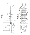
- FIG.1 is a circuit diagram of a related analog voltage output circuit, which includes an external connection terminal 1, such as a pad, an internal amplifier 2 formed of an operational amplifier serving as a voltage follower circuit, and an output protection circuit 3.
- the voltage output circuit shown in FIG.1 functions as a voltage follower circuit which converts a high input impedance into a low output impedance without changing the voltage.
- the output terminal OT and inverting input terminal IN(-) of the internal amplifier (operational amplifier) 2 are connected to the terminal 1 in the state where they are short-circuited.
- the output protection circuit 3 Since it is necessary to realize the low output impedance of the voltage output circuit, the output protection circuit 3 is provided which protects the internal amplifier 2 from an abnormal voltage Eh applied to the terminal 1 unexpectedly.
- the output protection circuit 3 has two diodes Da and Db, and two resistors Ra and Rb.
- the resistors Ra and Rb each having a low resistance, are connected in series between the terminal 1 and the output terminal of the internal amplifier 2.
- the diode Da is connected between the resistor Ra and ground GND
- the diode Db is connected between the resistor Rb and a power supply line set to a voltage Vcc higher than the ground potential.
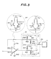
- FIG.2 illustrates a pattern of the output protection circuit 3.
- the resistor Ra is formed of a P-type impurity diffusion region 4 formed in a silicon substrate 7 of, for example, N type, and the resistor Rb is formed in a P-type well formed in an N-type impurity diffusion region 5 formed in the silicon substrate 7.
- the diffusion regions 4 and 5 are connected to a wiring (interconnection) layer 6 via contact holes 8.
- the diode Da is formed at a PN junction between the impurity diffusion region 4 and the silicon substrate 7, and the diode Db is formed at a PN junction between the impurity diffusion region 5 and the P-type well in the silicon substrate 7.
- the abnormal voltage Eh applied to the terminal 1 is attenuated by the resistor RA, and then discharged toward the ground GND via the diode Da. Further, the attenuated abnormal voltage Eh is attenuated by the resistor Rb, and then discharged toward the Vcc line through the diode Db. In this way, the internal amplifier circuit 2 has a high electrostatic breakdown voltage.
- the internal amplifier 2 since the internal amplifier 2 must have a low output impedance, it is impossible to form each of the resistors Ra and Rb of a resistor having a large resistance higher than, for example, 100 ohms. For this reason, there is a possibility that a charge q which has not passed through the diodes Da and Db and which has not been attenuated by the resistors Ra and Rb reaches the inverting input terminal IN(-) of the internal amplifier 2.
- the charge q inputs the internal amplifier 2, and may destroy the PN junction of a bipolar transistor forming the inverting input terminal or a gate of a field effect transistor of the internal amplifier 2 forming the inverting input terminal.
- the above problem occurs more frequently as the size of semiconductor elements becomes smaller or the gate insulating film becomes thinner.
- a protection circuit comprising: first protection means, coupled between a signal output terminal of an internal circuit and an external connection terminal, for preventing an abnormal voltage applied to the external connection terminal from being input to the signal output terminal; and second protection means, coupled between a signal input terminal of the internal circuit and the external connection terminal, for preventing the abnormal voltage applied to the external connection terminal from being input to the signal input terminal, the signal input terminal being operatively coupled to the signal output terminal via the first and second protection means and having an impedance higher than that of the signal output terminal.
- Another object of the present invention is to provide an integrated circuit device having the above-mentioned protection circuit.
- an integrated circuit device having the protection circuit which comprises: a semiconductor substrate having a first conduction type; an impurity diffusion region formed in the semiconductor substrate, the impurity diffusion region having a second conduction type different from the first conduction type; a first interconnection line which is in contact with the impurity diffusion region and which is coupled to the external connection terminal; and a second interconnection line which is in contact with the impurity diffusion region and which are electrically coupled to the signal input terminal.
- the impurity diffusion region forms a resistor, and a junction between the semiconductor substrate and the impurity diffusion region forms a diode.
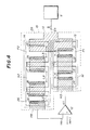
- FIG.3 shows a voltage follower circuit having an input/output protection circuit 15, which has a first protection circuit 13 and a second protection circuit 14.
- the voltage follower circuit shown in FIG.3 has an external connection terminal 11, such as a pad, and an internal amplifier 12.
- the internal amplifier 12 is formed of, for example, an operational amplifier, which includes bipolar transistors Q1 and Q2 or field effect transistors T1 and T2.
- a base B1 of the bipolar transistor Q1 functions as an inverting input terminal IN(-) of the internal amplifier, and a base B2 of the bipolar transistor Q2 functions as a non-inverting input terminal IN(+) thereof.
- a gate G1 of the field effect transistor T1 functions as the inverting input terminal IN(-) of the operational amplifier 12, and a gate G2 of the field effect transistor T2 functions as the non-inverting terminal IN(+) thereof.
- a predetermined signal is applied to the non-inverting terminal IN(+) of the internal amplifier 12.
- the operational amplifier 12 is connected between the Vcc line and the ground GND.
- the first protection circuit 13 has an input terminal connected to the output terminal OT of the internal circuit 12, and an output terminal connected to the terminal 11.
- the second protection circuit has an input terminal connected to the terminal 11, and an output terminal connected to the inverting input terminal IN(-) of the internal amplifier 12.
- the first protection circuit 13 is composed of two diodes D11 and D12, and two resistors R11 and R12.
- the diode D11 has an anode grounded and a cathode connected to the resistor R11.
- the diode D12 has an anode connected to the resistor R12 and a cathode connected to the Vcc line.
- the resistors R11 and R12 are connected in series between the output terminal OT of the internal amplifier 12 and the terminal 11. It is possible to omit the resistors R11 and R12 if parasitic loads are coupled between the output terminal OT of the internal amplifier 12 and the terminal 11. Such parasitic loads may be formed by lead electrodes of the diodes D11 and D12 or wiring lines thereof.
- the second protection circuit 14 is composed of two diodes D21 and D22, and two resistors R21 and R22.
- the diode D21 has an anode grounded and a cathode connected to the resistor R21.
- the diode D22 has an anode connected to the resistor R22 and a cathode connected to the Vcc line.
- the resistors R21 and R22 are connected in series between the terminal 11 and the inverting input terminal IN(-) of the internal amplifier 12.
- the sum of the resistance values of the resistors R11 and R12 be between zero ohm and a few of tens ohms.
- the sum of the resistance values of the resistors R21 and R22 must be larger than the sum of the resistance values of the resistors R11 and R12. It is preferable that each of the resistors R21 and R22 has a resistor at least ten to hundred times the resistance of each of the resistors R11 and R12.
- the internal amplifier 12 can operate as the voltage follower circuit.
- An input voltage Ei generated and output by a high-impedance circuit (not shown for the sake of simplicity) is applied to the non-inverting input terminal IN(+) of the internal amplifier 12, which amplifies the input voltage Ei and outputs an output voltage Eo to the resistors R12 and R11.
- the gain of the internal amplifier 12, Av is such that .
- the output voltage is then applied to the terminal 11 via the low-impedance circuit including the resistors R12 and R11.
- the above-mentioned state corresponds to an equivalent state where the output terminal and the inverting input terminal IN(-) of the internal amplifier 12 are short-circuited.
- the first protection circuit 13 protects an output transistor of the operational amplifier 12 forming the output terminal OT thereof from the abnormal voltage Eh.
- the charge of the abnormal voltage Eh is allowed to flow to the Vcc line or ground through the diodes D12 or D11.
- the second protection circuit 14 protects the transistor Q1 or T1 of the internal amplifier 12 from the abnormal voltage Eh.
- the charge of the abnormal voltage Eh is attenuated by the resistors R21 and R22 and allow to flow to the Vcc line or ground through the diode D21 or D22. Thus, no abnormal voltage is input to the inverting input terminal IN(-) of the internal amplifier 12.
- the signal obtained at the terminal 11 is fed back to the inverting input terminal IN(-) of the internal amplifier 12.
- voltage drops respectively developed across the resistors R11 and R12 are canceled.
- the signal of the output terminal OT of the internal amplifier 2 shown in FIG.1 is fed back to the inverting input terminal IN(-) of the internal amplifier 2.
- the voltage of the external terminal 1 is affected by the voltage drops respectively developed across the resistors Ra and Rb.
- FIG.4 shows a pattern of resistors including the resistors R11, R12, R21 and R22 of the input/output protection circuit 15.
- the patterns of the first and second protection circuits 13 and 14 are close to the terminal 11. As these patterns are closer to the terminal 11, the abnormal voltage 11 can be canceled more rapidly.
- the first and second protection circuits 13 and 14 are formed in a silicon substrate 25.
- the first protection circuit 13 has a P-type impurity diffusion region P1 and an N-type impurity diffusion region N1.
- the P-type impurity diffusion region P1 is electrically in contact with aluminum wiring (interconnection) layers H1 and H2 through contact holes J1 and J2 formed in an insulating film (not shown), respectively.
- the wiring layer H1 is connected to the terminal 11.
- the N-type impurity diffusion region N1 is electrically in contact with wiring layers H2 and H3 via contact holes J3 and J4 formed in the insulating film, respectively.
- the wiring layer H2 electrically connects the P-type impurity diffusion region P1 and the N-type impurity diffusion region N1.
- the wiring layer H3 is connected to the output terminal OT of the internal amplifier 12.
- the second protection circuit 14 has a P-type impurity diffusion region P2, an N-type impurity diffusion region N2 and a high-resistance region 26.
- the P-type impurity diffusion region P2 is electrically in contact with the wiring layer H1 through a contact hole J5 formed in the insulating layer, and in contact with an aluminum wiring layer H4 through a contact hole J6.
- the N-type impurity diffusion layer N2 is electrically in contact with the wiring layer H4 through a contact hole J7 as well as an aluminum wiring layer H5 through a contact hole J8.
- the high-resistance layer 26 is electrically in contact with the wiring layer H5 through a contact hole J9 as well as an aluminum wiring layer H6 through a contact hole J10.
- the wiring layer H6 is connected to the inverting input terminal IN(-) of the internal amplifier 12. It will be seen from the above that the second protection circuit 14 has three resistors connected in series.
- the resistors R11 and R12 may have an identical resistance or different resistances.
- the resistors R21 and R22 may have an identical resistance of different resistances.
- the diode D11 is formed at a junction between the P-type impurity diffusion layer P1 and the silicon substrate 25, and the diode D12 is formed at a junction between the N-type impurity diffusion layer N1 and a P-type well (not shown for the sake of simplicity) formed in the silicon substrate 25 when it is of the N type.
- the diode D21 is formed at a junction between the P-type impurity diffusion layer P2 and the silicon substrate 25, and the diode D22 is formed at a junction between the N-type impurity diffusion region N2 and the P-type well.
- the abnormal voltage Eh applied to the terminal 11 is transferred to the P-type impurity diffusion regions P1 and P2 via the wiring line H1, and attenuated (absorbed) therein.
- the charges of the abnormal voltage Eh flow to the ground via the diodes D11 and D21.
- the remaining charges are transferred to the N-type impurity diffusion regions N1 and N2, and attenuated therein.
- the remaining charges flow to the Vcc line via the diodes D12 and D22.
- the still remaining charges are attenuated in the high-resistance region 26.
- the inverting input terminal and the output terminal of the internal amplifier 12 are not affected by the existence of the abnormal voltage Eh.
- the first protection circuit 13 can be composed of an arbitrary number of resistors and diodes.
- the second protection circuit 14 can be composed of an arbitrary number of resistors and diodes. As shown in FIG.5, the first protection circuit 13 is composed of m resistors R31, R32, ..., R3m, and m diodes D31, D32, ..., D3m where m is an integer.
- the second protection circuit 14 is composed of n resistors R41, R42, ..., R4n, and n diodes D41, D42, ..., D4n where n is an integer.
- the diodes D32, ..., D3m of the first protection circuit 13 have anodes grounded and cathodes connected to the resistors R32, ..., R3m.
- the diodes D42, ..., D4n of the second protection circuit 14 have anodes grounded and cathodes connected in the resistors R42, ..., R4n, respectively.
- the number of resistors in each of the first and second protection circuits 13 and 14 may be different from that of diodes.
- FIG.6A shows another pattern of the first and second protection circuits 13 and 14 shown in FIG.3, and FIG. 6B is a cross-sectional view taken along line VI B -VI B shown in FIG.6A.
- the first protection circuit 13 has a P-type impurity diffusion region P11 formed in the silicon substrate 25 of the N type, and an N-type impurity diffusion region N11 formed in a P-type well 41 formed in the silicon substrate 25.
- An aluminum wiring layer H11 connected to the terminal (pad) 11 is in contact with the P-type impurity diffusion region P11 through contact holes J11 formed in an insulating film 32.
- the P-type impurity diffusion region P11 and the N-type impurity diffusion region N11 are electrically connected trough an aluminum wiring line H12, which is electrically in contact with the P-type impurity diffusion region P11 through contact holes J12 formed in the insulating film 32 and the N-type impurity diffusion region N11 through contact holes J13 formed therein.
- the N-type impurity diffusion region N11 is electrically connected to the output terminal OT of the internal amplifier 12 via an aluminum wiring layer H13, which is electrically in contact with the N-type impurity diffusion region N11 via contact holes J14 formed in the insulating film 32.
- the second protection circuit 14 has a P-type impurity diffusion region P12 formed in the silicon substrate 25, and an N-type impurity diffusion region N12 formed in the P-type well 41.
- the wiring layer H11 connects the terminal 11 to the P-type impurity diffusion region P12, which is electrically in contact with the wiring layer H11 through contact holes J15.
- An aluminum wiring line H14 which is electrically in contact with the P-type impurity diffusion region P12 through contact holes J16, is in contact with the N-type impurity diffusion region N12 via contact holes J17.
- An aluminum wiring line H15 which is in contact with the N-type impurity diffusion region N12, is connected to the inverting input terminal of the internal amplifier 12.
- a reference 31 indicates a well contact.
- a P-type impurity diffusion region is provided in the P-type well 41, as shown in FIG.6B.
- An N-type impurity diffusion region (Vcc) is provided in the silicon substrate 25, as shown in FIG.6B.
- diodes are formed at PN junctions.
- the second embodiment shown in FIG.7 includes a digital-to-analog (D/A) converter 50, a constant voltage generation circuit 60, and the aforementioned input/output protection circuit 15.
- the D/A converter 50 is composed of a resistors 511 - 518 connected in series, a switch SW and an operational amplifier 52.
- the inverting input terminal of the operational amplifier 52 is directly connected to the output terminal thereof.
- a control signal generated by an internal circuit (not shown) of the D/A converter 50 is applied to the switch SW so that the switch SW selects one of stationary contacts connected to respective connection nodes where adjacent resistors are connected.
- the constant voltage generation circuit 60 includes a resistor 61 and a Zener diode 62 connected in series between the Vcc line and ground. Conventionally, a constant voltage is directly applied to the non-inverting input terminal of the operational amplifier 52. In order to examine whether or not the constant voltage generation circuit 60 generates a predetermined constant voltage, conventionally, the terminal 11 is directly connected between the constant voltage generation circuit 60 and the non-inverting input terminal of the operational amplifier 52.
- the second embodiment of the present invention has the input/output protection circuit 15 provided between the terminal 11 and the constant voltage generation circuit 60 and also between the terminal 11 and the non-inverting terminal of the operational amplifier 52.
- An abnormal voltage applied to the terminal 11 is canceled by the input/output protection circuit 15, so that the operational amplifier 52 is not affected by the abnormal voltage.
Landscapes
- Engineering & Computer Science (AREA)
- Power Engineering (AREA)
- Semiconductor Integrated Circuits (AREA)
- Amplifiers (AREA)
Applications Claiming Priority (2)
| Application Number | Priority Date | Filing Date | Title |
|---|---|---|---|
| JP111414/90 | 1990-04-26 | ||
| JP2111414A JP2838836B2 (ja) | 1990-04-26 | 1990-04-26 | 半導体集積回路及び半導体集積回路装置 |
Publications (3)
| Publication Number | Publication Date |
|---|---|
| EP0454091A2 true EP0454091A2 (de) | 1991-10-30 |
| EP0454091A3 EP0454091A3 (en) | 1991-11-27 |
| EP0454091B1 EP0454091B1 (de) | 1994-10-19 |
Family
ID=14560567
Family Applications (1)
| Application Number | Title | Priority Date | Filing Date |
|---|---|---|---|
| EP91106606A Expired - Lifetime EP0454091B1 (de) | 1990-04-26 | 1991-04-24 | Ein-/Ausgangsschutzschaltung und Halbleiterbauelement mit dieser Schaltung |
Country Status (5)
| Country | Link |
|---|---|
| US (1) | US5650652A (de) |
| EP (1) | EP0454091B1 (de) |
| JP (1) | JP2838836B2 (de) |
| KR (1) | KR950003910B1 (de) |
| DE (1) | DE69104642T2 (de) |
Cited By (2)
| Publication number | Priority date | Publication date | Assignee | Title |
|---|---|---|---|---|
| WO2009102448A1 (en) * | 2008-02-15 | 2009-08-20 | Analog Devices, Inc. | Differential current output driver with overvoltage protection |
| US7813093B2 (en) | 2008-02-15 | 2010-10-12 | Analog Devices, Inc. | Output driver with overvoltage protection |
Families Citing this family (6)
| Publication number | Priority date | Publication date | Assignee | Title |
|---|---|---|---|---|
| JPH1146120A (ja) * | 1997-07-25 | 1999-02-16 | Mitsubishi Electric Corp | 差動増幅回路 |
| US6309245B1 (en) | 2000-12-18 | 2001-10-30 | Powerwave Technologies, Inc. | RF amplifier assembly with reliable RF pallet ground |
| DE10248149B4 (de) * | 2002-10-15 | 2011-09-29 | Lantiq Deutschland Gmbh | Treiberschaltung mit frequenzabhängiger Signalrückkopplung |
| JP5550844B2 (ja) * | 2009-03-30 | 2014-07-16 | ラピスセミコンダクタ株式会社 | 半導体集積回路 |
| KR101876439B1 (ko) * | 2017-01-02 | 2018-07-10 | 동서대학교산학협력단 | 조립식 블록형 회로설계를 위한 기능형 아날로그 모듈, 그리고 이를 포함하는 조립식 블록형 회로설계 모듈 시스템 |
| US12278625B2 (en) * | 2020-07-21 | 2025-04-15 | Nippon Telegraph And Telephone Corporation | Driver circuit |
Family Cites Families (5)
| Publication number | Priority date | Publication date | Assignee | Title |
|---|---|---|---|---|
| US4066918A (en) * | 1976-09-30 | 1978-01-03 | Rca Corporation | Protection circuitry for insulated-gate field-effect transistor (IGFET) circuits |
| NL8100242A (nl) * | 1981-01-20 | 1982-08-16 | Philips Nv | Overspanningsbeveiliging van een lijncircuit. |
| JPS6132464A (ja) * | 1984-07-24 | 1986-02-15 | Nec Corp | Cmos型集積回路装置 |
| JPS6325976A (ja) * | 1986-07-18 | 1988-02-03 | Toshiba Corp | 半導体装置の製造方法 |
| US4990802A (en) * | 1988-11-22 | 1991-02-05 | At&T Bell Laboratories | ESD protection for output buffers |
-
1990
- 1990-04-26 JP JP2111414A patent/JP2838836B2/ja not_active Expired - Fee Related
-
1991
- 1991-04-24 EP EP91106606A patent/EP0454091B1/de not_active Expired - Lifetime
- 1991-04-24 DE DE69104642T patent/DE69104642T2/de not_active Expired - Fee Related
- 1991-04-26 KR KR1019910006777A patent/KR950003910B1/ko not_active Expired - Fee Related
-
1996
- 1996-07-26 US US08/687,832 patent/US5650652A/en not_active Expired - Fee Related
Cited By (5)
| Publication number | Priority date | Publication date | Assignee | Title |
|---|---|---|---|---|
| WO2009102448A1 (en) * | 2008-02-15 | 2009-08-20 | Analog Devices, Inc. | Differential current output driver with overvoltage protection |
| US7813093B2 (en) | 2008-02-15 | 2010-10-12 | Analog Devices, Inc. | Output driver with overvoltage protection |
| CN101971488A (zh) * | 2008-02-15 | 2011-02-09 | 阿纳洛格装置公司 | 具有过压保护的差分电流输出驱动器 |
| US7957111B2 (en) | 2008-02-15 | 2011-06-07 | Analog Devices, Inc. | Differential current output driver with overvoltage protection |
| CN101971488B (zh) * | 2008-02-15 | 2013-05-29 | 美国亚德诺半导体公司 | 具有过压保护的差分电流输出驱动器 |
Also Published As
| Publication number | Publication date |
|---|---|
| DE69104642T2 (de) | 1995-05-04 |
| EP0454091A3 (en) | 1991-11-27 |
| KR910019332A (ko) | 1991-11-30 |
| EP0454091B1 (de) | 1994-10-19 |
| KR950003910B1 (ko) | 1995-04-20 |
| US5650652A (en) | 1997-07-22 |
| DE69104642D1 (de) | 1994-11-24 |
| JP2838836B2 (ja) | 1998-12-16 |
| JPH048003A (ja) | 1992-01-13 |
Similar Documents
| Publication | Publication Date | Title |
|---|---|---|
| US5781389A (en) | Transistor protection circuit | |
| KR100237262B1 (ko) | 반도체 장치내에서 사용하기 위한 입력/출력 보호장치 | |
| US6442008B1 (en) | Low leakage clamp for E.S.D. protection | |
| US7692492B2 (en) | Operational amplifier | |
| US20090026493A1 (en) | Electrostatic Protection Circuit | |
| US6239958B1 (en) | Electrostatic damage protection circuit and dynamic random access memory | |
| JPH03111916A (ja) | 電流制御回路 | |
| JP2002124573A (ja) | 集積回路のための入力段esd保護 | |
| EP0454091B1 (de) | Ein-/Ausgangsschutzschaltung und Halbleiterbauelement mit dieser Schaltung | |
| JP4843927B2 (ja) | 高周波集積回路 | |
| JPH11251530A (ja) | 半導体装置 | |
| US12567739B2 (en) | Electrostatic protection circuit | |
| US7110232B2 (en) | Semiconductor circuit with protective circuit | |
| KR0145642B1 (ko) | 반도체 장치 | |
| EP0042581A2 (de) | Integrierte Schaltung | |
| JP3019760B2 (ja) | 半導体集積回路装置 | |
| JP2636804B2 (ja) | 半導体装置 | |
| US11244941B2 (en) | Integrated device for protection from electrostatic discharges | |
| US6813130B2 (en) | Semiconductor integrated circuit device including protection circuit for preventing circuit breakdown by static electricity | |
| US7746611B2 (en) | ESD protective circuit having low leakage current | |
| US20050264964A1 (en) | Semiconductor circuit | |
| US6433407B2 (en) | Semiconductor integrated circuit | |
| US5767537A (en) | Capacitively triggered silicon controlled rectifier circuit | |
| US5903184A (en) | Semiconductor device having protection circuit | |
| JP4099343B2 (ja) | 半導体装置 |
Legal Events
| Date | Code | Title | Description |
|---|---|---|---|
| PUAI | Public reference made under article 153(3) epc to a published international application that has entered the european phase |
Free format text: ORIGINAL CODE: 0009012 |
|
| PUAL | Search report despatched |
Free format text: ORIGINAL CODE: 0009013 |
|
| AK | Designated contracting states |
Kind code of ref document: A2 Designated state(s): DE FR GB |
|
| AK | Designated contracting states |
Kind code of ref document: A3 Designated state(s): DE FR GB |
|
| 17P | Request for examination filed |
Effective date: 19911216 |
|
| 17Q | First examination report despatched |
Effective date: 19930316 |
|
| GRAA | (expected) grant |
Free format text: ORIGINAL CODE: 0009210 |
|
| AK | Designated contracting states |
Kind code of ref document: B1 Designated state(s): DE FR GB |
|
| REF | Corresponds to: |
Ref document number: 69104642 Country of ref document: DE Date of ref document: 19941124 |
|
| RIN2 | Information on inventor provided after grant (corrected) |
Free format text: MIZUTANI, TORU * KOBAYASHI, OSAMU * GOTOH, KUNIHIKO |
|
| ET | Fr: translation filed | ||
| PLBE | No opposition filed within time limit |
Free format text: ORIGINAL CODE: 0009261 |
|
| STAA | Information on the status of an ep patent application or granted ep patent |
Free format text: STATUS: NO OPPOSITION FILED WITHIN TIME LIMIT |
|
| 26N | No opposition filed | ||
| REG | Reference to a national code |
Ref country code: GB Ref legal event code: IF02 |
|
| PGFP | Annual fee paid to national office [announced via postgrant information from national office to epo] |
Ref country code: FR Payment date: 20080312 Year of fee payment: 18 Ref country code: DE Payment date: 20080502 Year of fee payment: 18 |
|
| PGFP | Annual fee paid to national office [announced via postgrant information from national office to epo] |
Ref country code: GB Payment date: 20080430 Year of fee payment: 18 |
|
| GBPC | Gb: european patent ceased through non-payment of renewal fee |
Effective date: 20090424 |
|
| REG | Reference to a national code |
Ref country code: FR Ref legal event code: ST Effective date: 20091231 |
|
| PG25 | Lapsed in a contracting state [announced via postgrant information from national office to epo] |
Ref country code: DE Free format text: LAPSE BECAUSE OF NON-PAYMENT OF DUE FEES Effective date: 20091103 |
|
| PG25 | Lapsed in a contracting state [announced via postgrant information from national office to epo] |
Ref country code: GB Free format text: LAPSE BECAUSE OF NON-PAYMENT OF DUE FEES Effective date: 20090424 Ref country code: FR Free format text: LAPSE BECAUSE OF NON-PAYMENT OF DUE FEES Effective date: 20091222 |