EP0453997B1 - Halbleiter-Speichereinrichtung - Google Patents
Halbleiter-Speichereinrichtung Download PDFInfo
- Publication number
- EP0453997B1 EP0453997B1 EP91106361A EP91106361A EP0453997B1 EP 0453997 B1 EP0453997 B1 EP 0453997B1 EP 91106361 A EP91106361 A EP 91106361A EP 91106361 A EP91106361 A EP 91106361A EP 0453997 B1 EP0453997 B1 EP 0453997B1
- Authority
- EP
- European Patent Office
- Prior art keywords
- resistance
- power source
- memory
- lines
- memory cells
- Prior art date
- Legal status (The legal status is an assumption and is not a legal conclusion. Google has not performed a legal analysis and makes no representation as to the accuracy of the status listed.)
- Expired - Lifetime
Links
- 239000004065 semiconductor Substances 0.000 title claims description 29
- 229910021420 polycrystalline silicon Inorganic materials 0.000 description 8
- 229920005591 polysilicon Polymers 0.000 description 8
- 238000010586 diagram Methods 0.000 description 6
- 238000000034 method Methods 0.000 description 5
- 230000003068 static effect Effects 0.000 description 5
- 239000002184 metal Substances 0.000 description 3
- 230000000694 effects Effects 0.000 description 2
- 238000004519 manufacturing process Methods 0.000 description 2
- 230000002093 peripheral effect Effects 0.000 description 2
- 230000002950 deficient Effects 0.000 description 1
- 230000014759 maintenance of location Effects 0.000 description 1
Images


Classifications
-
- G—PHYSICS
- G11—INFORMATION STORAGE
- G11C—STATIC STORES
- G11C11/00—Digital stores characterised by the use of particular electric or magnetic storage elements; Storage elements therefor
- G11C11/21—Digital stores characterised by the use of particular electric or magnetic storage elements; Storage elements therefor using electric elements
- G11C11/34—Digital stores characterised by the use of particular electric or magnetic storage elements; Storage elements therefor using electric elements using semiconductor devices
- G11C11/40—Digital stores characterised by the use of particular electric or magnetic storage elements; Storage elements therefor using electric elements using semiconductor devices using transistors
- G11C11/41—Digital stores characterised by the use of particular electric or magnetic storage elements; Storage elements therefor using electric elements using semiconductor devices using transistors forming static cells with positive feedback, i.e. cells not needing refreshing or charge regeneration, e.g. bistable multivibrator or Schmitt trigger
-
- G—PHYSICS
- G11—INFORMATION STORAGE
- G11C—STATIC STORES
- G11C5/00—Details of stores covered by group G11C11/00
- G11C5/14—Power supply arrangements, e.g. power down, chip selection or deselection, layout of wirings or power grids, or multiple supply levels
-
- G—PHYSICS
- G11—INFORMATION STORAGE
- G11C—STATIC STORES
- G11C11/00—Digital stores characterised by the use of particular electric or magnetic storage elements; Storage elements therefor
- G11C11/21—Digital stores characterised by the use of particular electric or magnetic storage elements; Storage elements therefor using electric elements
- G11C11/34—Digital stores characterised by the use of particular electric or magnetic storage elements; Storage elements therefor using electric elements using semiconductor devices
- G11C11/40—Digital stores characterised by the use of particular electric or magnetic storage elements; Storage elements therefor using electric elements using semiconductor devices using transistors
- G11C11/41—Digital stores characterised by the use of particular electric or magnetic storage elements; Storage elements therefor using electric elements using semiconductor devices using transistors forming static cells with positive feedback, i.e. cells not needing refreshing or charge regeneration, e.g. bistable multivibrator or Schmitt trigger
- G11C11/413—Auxiliary circuits, e.g. for addressing, decoding, driving, writing, sensing, timing or power reduction
- G11C11/417—Auxiliary circuits, e.g. for addressing, decoding, driving, writing, sensing, timing or power reduction for memory cells of the field-effect type
Definitions
- the present invention relates to a semiconductor memory device and is applicable to a semiconductor memory device used for controlling power consumption of an IC on which a high-resistance load type static RAM and a logic circuit are mounted.
- US-A-3 621 302 describes a semiconductor device formed on a semiconductor chip, comprising:
- the circuit is also provided with a resistor connected across the switching transistor so that the standby or leakage current continues to flow even when the transistor is in its off state.
- GB-A-2 067 836 describes a memory device having a spare memory circuit provided only when needed.
- E/R type static RAM Enhancement/Resistor type static RAM to be referred to as "E/R type SRAM” hereinafter
- V DD denotes a positive power source voltage
- V SS a ground power source voltage
- R a high-resistance load
- Tr1 and Tr2 transferring gates constituted by n-channel MOS transistors
- Tr3 and Tr4 driver transistors constituted by n-channel MOS transistors
- B and B ⁇ bit lines
- W word lines.
- the high-resistance load R used in the memory cell of the E/R type SRAM is constituted by a second polysilicon layer to decrease an area occupied by the memory cell.
- This can be achieved by a two-layer polysilicon technique in which the gate electrodes of the MOS transistors are constituted by a first polysilicon layer, and the high-resistance load R is constituted by the second polysilicon layer.
- I R data retention current (standby current, to be referred to as "leakage current” hereinafter) I R is changed according to the resistance of the high-resistance load R, the resistance generally has a large value.
- the E/R type SRAM is integrated at a high density.
- the first polysilicon layer is used as the gate electrodes of the MOS transistors Tr1 to Tr4, and the high-resistance load R can be formed by the second polysilicon layer formed on the MOS transistors Tr1 to Tr4.
- a relatively small leakage current I R can be obtained by a technique for increasing the resistance of the polysilicon layer. Therefore, in the above load cell, it is generally advantageous that the load R has a resistance as high as possible. Note that, at present, an increase in resistance of the load R is a required condition for obtaining a large-capacity memory.
- each memory cell in order to obtain a leakage current I R of several ⁇ A (micro ampere), each memory cell is required to have a load resistance of several tera ohms (10 12 ⁇ ) or more.
- a resistance of several tera ohms or more is difficult to always obtain, and the leakage current I R has variations in the range of several ⁇ A to several hundred ⁇ A, i.e., the maximum variation being hundred times or more the minimum variation.
- power source voltages V DD and V SS of a logic section 11 and power source voltages V DD and V SS in a memory section 12 of the E/R type SRAM are generally applied from the same power source pads 13a and 13b. Therefore, when the power consumption of a semiconductor chip 14 is evaluated, the power consumption of all the E/R type SRAM and the logic section must be evaluated. A total current is evaluated at present.
- a variation in the leakage current I R from a memory section 12 of the E/R type SRAM is larger than that of a leakage current from the logic section 11. That is, when a total leakage current of the semiconductor chip 14 is evaluated, since the static current consumption of the logic section 11 is generally about 100 ⁇ A, the leakage current from the logic section 11 and a current obtained by varying the leakage current I R from the memory section 12 of the E/R type SRAM cannot be distinguished from each other.
- the logic section 11 and the memory section 12 of the E/R type SRAM have different device arrangements, and a defective device may be formed in manufacturing.
- the logic section 11 and the memory section 12 must be independently discriminated from each other. Therefore, the independent discrimination of errors of leakage currents from the logic section 11 and the memory section 12 of the E/R type SRAM is one of the important factors. However, in a conventional circuit arrangement, this independent discrimination cannot be performed.
- an object of the present invention to provide a semiconductor memory device capable of independently discriminating and evaluating leakage currents from a memory section of a large-capacitance E/R type SRAM and a logic section, and cutting off an unnecessary leakage current during the use of the memory device.
- a semiconductor device in which a memory section and a logic section are formed on the same semiconductor chip, comprising:
- said switching elements are MOS transistors each having a low ON resistance.
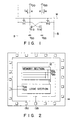
- Fig. 3 shows a semiconductor memory device according to the first embodiment of the present invention.
- Reference numeral 1 denotes a memory section of an E/R type SRAM. That is, n memory cells M 1 , M 2 ..., M n are arranged in the memory section 1 in an array form.
- a memory cell array is constituted by the memory cells M 1 , M 2 ..., M n .
- a sense amplifier section 2 and a precharging section 3 are formed as peripheral circuits.
- high-resistance elements R 1 , R 2 , ..., R n of the n memory cells M 1 , M 2 , ..., M n are connected to predetermined nodes X 1 , X 2 , ..., X n , respectively.
- the nodes X 1 , X 2 , ..., X n are connected to a terminal K by a low-resistance line L.
- a switching element e.g., a MOS transistor
- Sw having an ON resistance (10 2 to 10 4 ⁇ or less) much lower than those of the high-resistance elements (resistances of 10 10 to 10 12 ⁇ or less) R 1 , R 2 , ..., R n of the memory cells M 1 , M 2 , ..., M n is connected between the terminal K and a power source line Lv1.
- the switching element Sw is used for disconnecting the n memory cells M 1 , M 2 , ..., M n from the power source line Lv1 by a control signal Tc from a control circuit (not shown) as needed.
- the switching element Sw having an ON resistance very lower than those of the high-resistance elements R 1 , R 2 , ..., R n of the memory cells M 1 , M 2 , ..., M n is connected between the terminal K and the power source line Lv1. For this reason, when a leakage current is evaluated, the n memory cells M 1 , M 2 , ..., M n can be disconnected from the power source line Lv1, and leakage currents in parts except for the memory cells M 1 , M 2 , ..., M n of the E/R type SRAM can be evaluated.
- the switching element Sw is constituted by, e.g., a MOS transistor having an very low ON resistance (10 2 to 10 4 ⁇ or less), the switching element Sw can be laid out while the pattern area of the switching element Sw does not influence the chip area. That is, the switching element Sw can be obtained by a current process technique.
- Fig. 4 shows a semiconductor memory device according to the second embodiment of the present invention.
- a memory cell array 4 constituted by arranging n ⁇ m memory cells in an array form is formed in a memory section 1.
- a sense amplifier section 2 and a precharge section 3 are formed as peripheral circuits.
- the high-resistance elements (not shown) of the n ⁇ m memory cells arranged in an array form are connected to predetermined terminals K 1 to K m by predetermined low-resistance lines L 1 to L m , respectively. That is, the low-resistance lines L 1 to L m are arranged parallel to word lines W 1 to W m and vertically to bit lines B 1 to B n , and B 1 ⁇ to B n ⁇ .
- the low-resistance lines L 1 to L m are provided in units of the word lines W 1 to W m and connected to the high-resistance elements of the memory cells commonly connected to the word lines W 1 to W m . That is, one low-resistance line is provided to one word line, and one low-resistance line is connected to the high-resistance elements of the memory cells connected to the same word line.
- switching elements Swl to Swm each having an ON resistance (10 2 to 10 4 ⁇ or less) much lower than that of a high-resistance element (resistance of 10 10 to 10 12 ⁇ ) of a memory cell are connected between terminals K 1 to K m and a power source line Lv1.
- a Switching circuit 5 is constituted by the switching elements Sw1 to Swm.
- the opening/closing of the switching elements Sw1 to Swm is controlled by a control signal from a control circuit (e.g., decoder) 6.
- a control circuit e.g., decoder
- the switching elements Sw1 to Swm are simultaneously ON/OFF-controlled, and an arbitrary number of elements may be ON/OFF-controlled.
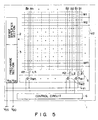
- Fig. 5 shows a semiconductor memory device according to the third embodiment of the present invention.
- a memory cell array 4 obtained by arranging n ⁇ m memory cells in an array form is formed on a memory cell section 1.
- the high-resistance elements (not shown) of the n ⁇ m memory cells are connected to predetermined terminals K 1 to K n by low-resistance lines L 1 to L n , respectively. That is, the low-resistance lines L 1 to L m are arranged parallelly to bit lines B 1 to B n and B 1 ⁇ to B n ⁇ and vertically to word lines W 1 to W m .
- the low-resistance lines L 1 to L n are provided in units of the bit lines B 1 to B n and B 1 ⁇ to B n ⁇ and connected to the high-resistance elements of the memory cells commonly connected to the bit lines B 1 to B n and B 1 ⁇ to B n ⁇ . That is, one low-resistance line is provided to one bit line, and one low-resistance line is connected to the high-resistance elements of the memory cells connected to the same bit line.
- switching elements Sw1 to Swn each having an ON resistance (10 2 to 10 4 ⁇ or less) much lower than that of a high-resistance element resistance of 10 10 to 10 12 ⁇ ) of a memory cell are connected between terminals K 1 to K n and a power source line Lv1.
- a switching circuit 5 is constituted by the switching elements Sw1 to Swm.
- the opening/closing of the switching elements Sw1 to Swm is controlled by a control signal from a control circuit (e.g., decoder) 6.
- the switching elements Sw1 to Swm are simultaneously ON/OFF-controlled, and an arbitrary number of elements may be ON/OFF-controlled.
- the switching elements Sw1 to Swm and Sw1 to Swn are arranged to each of low-resistance lines L 1 to L m and L 1 to L n arranged in units of the word lines W 1 to W m and the bit lines B 1 to B n and B 1 ⁇ to B n ⁇ , respectively.
- a power source V DD
- V DD can be disconnected from memory cells in unit of memory cells commonly connected to the word lines W 1 to W m and the bit lines B 1 to B n and B 1 ⁇ to B n ⁇ .
- This arrangement is effective in a device in which a predetermined area must be assured due to layout limitations in a cell shape having a predetermined underlying (transistor section), as shown in an entire surface element type gate array. For example, when an underlying region for a 64-kbit memory is assured, memory elements are arranged regardless of use/nonuse of a memory cell. However, since the switching elements Sw1 to Swm and Sw1 to Swn are arranged, a leakage current from only a nonused portion can be cut off during the use of the device. Therefore, the device can be used with minimum power consumption.
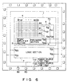
- Fig. 6 is a sectional view showing a semiconductor memory device according to the fourth embodiment of the present invention mounted on a chip.
- power source voltages V DD and V SS in a memory section 1 and power source voltages V DD and V SS in a logic section 7 are applied from the same power source pads 8a and 8b.
- a switching element Sw is connected between a memory cell array 4 of the memory section 1 and a power source (V DD ) line Lv1.
- the switching element Sw is ON/OFF-controlled by a control signal Tc from a control circuit (e.g., decoder).
- metal lines may be used.
- the metal line connected to a nonused memory cell can be disconnected from the power source line Lv1 by a laser beam, and a leakage current from the nonused portion can be cut off.
- a switching element having an ON resistance lower than that of a high-resistance element is connected between a memory cell and a power source. For this reason, the switching element is ON/OFF-controlled to disconnect the memory cell from the power source. Therefore, in a large-capacity E/R type SRAM, leakage currents generated from a memory cell section and a logic section can be independently discriminated and evaluated. In addition, when the E/R type SRAM is used, since only a nonused memory core section can be disconnected from a power source line, the semiconductor memory device can be used while an unnecessary leakage current is cut off.
- a switching element is connected between the line connected to a high-resistance element and a power source in a memory cell. For this reason, the switching element is ON/OFF-controlled to be able to disconnect all memory cells from the power source. Therefore, even in a large-capacity E/R type SRAM, a leakage current generated from a memory section and a leakage current generated from a logic section can be independently discriminated and evaluated.
- the semiconductor memory device since only a nonused memory cell can be separated from a power source, the semiconductor memory device can be used while an unnecessary leakage current is cut off.
Landscapes
- Engineering & Computer Science (AREA)
- Microelectronics & Electronic Packaging (AREA)
- Computer Hardware Design (AREA)
- Power Engineering (AREA)
- Semiconductor Memories (AREA)
- Static Random-Access Memory (AREA)
- For Increasing The Reliability Of Semiconductor Memories (AREA)
- Testing Or Measuring Of Semiconductors Or The Like (AREA)
Claims (2)
- Halbleitereinrichtung, in der ein Speicherabschnitt und ein Logikabschnitt auf demselben Halbleiterchip gebildet werden, enthaltend:ein Speicherzellenfeld (4), das durch Anordnen von Speicherzellen mit einem Flip-Flop mit Elementen mit relativ hohem Widerstand in Feldform erhalten wird, wobei jede Speicherzelle von dem Typ ist, der einen Standby- oder Leckstrom während des normalen Einsatzes führt;mehrere Wortleitungen (W1, W1, ..., Wm) und mehrere Bitleitungspaare (B1, /B1, B2, /B2, ..., Bn, /Bn) zum Adressieren der Speicherzellen des Speicherzellenfelds;mehrere Leitungen (L1, L2, ..., Lm) mit relativ niedrigem Widerstand, die rechtwinklig zu oder in Entsprechung mit und entlang der Wortleitungen (W1, W2, ..., Wm) angeordnet sind und die parallel zu oder rechtwinklig zu den Bitleitungspaaren (B1, /B1, B2, /B2, ..., Bn, /Bn) angeordnet sind und die als Stromversorgungsleitungen der Speicherzellen dienen und die mit den Elementen mit relativ hohem Widerstand verbunden sind; undeine Stromversorgungsleitung (Lv1, Lv2), die alsStromversorgungspfad für ein Stromversorgungspad dient;gekennzeichnet durcheine Umschalt-Schaltung (5), die durch mehrere Schaltelemente (Sw1, Sw2 ..., Swm) gebildet ist, die jeweils zwischen den Leitungen (L1, L2, ..., Lm) mit relativ niedrigem Widerstand und der Stromversorgungsleitung (Lv1) ausgebildet sind, wobei die mehreren Schaltelemente (Sw1, Sw2 ..., Swm) so betreibbar sind, daß sie den Leck- oder Standby-Strom zwischen den Leitungen (L1, L2, ..., Lm) mit relativ niedrigem Widerstand und der Stromversorgungsleitung (Lv1) während einem abgeschalteten Zustand der Schaltelemente (Sw1, Sw2 ..., Swm) unterbrechen; undeine Steuerschaltung (6) zum Steuern der Umschalt-Schaltung (5) zum Unterbrechen des Leck- oder Standby-Stroms für sämtliche Speicherzellen des Felds, wodurch der von dem Logikabschnitt erzeugte Leckstrom unabhängig unterscheidbar und bewertbar ist.
- Einrichtung nach Anspruch 1, dadurch gekennzeichnet, daß die Umschaltelemente (Sw1, Sw2 ..., Swm) MOS-Transistoren jeweils mit einem geringen Anschalt-Widerstand sind.
Applications Claiming Priority (2)
| Application Number | Priority Date | Filing Date | Title |
|---|---|---|---|
| JP2105908A JP2723338B2 (ja) | 1990-04-21 | 1990-04-21 | 半導体メモリ装置 |
| JP105908/90 | 1990-04-21 |
Publications (2)
| Publication Number | Publication Date |
|---|---|
| EP0453997A1 EP0453997A1 (de) | 1991-10-30 |
| EP0453997B1 true EP0453997B1 (de) | 1997-02-19 |
Family
ID=14419971
Family Applications (1)
| Application Number | Title | Priority Date | Filing Date |
|---|---|---|---|
| EP91106361A Expired - Lifetime EP0453997B1 (de) | 1990-04-21 | 1991-04-19 | Halbleiter-Speichereinrichtung |
Country Status (5)
| Country | Link |
|---|---|
| US (1) | US5355331A (de) |
| EP (1) | EP0453997B1 (de) |
| JP (1) | JP2723338B2 (de) |
| KR (1) | KR950006425B1 (de) |
| DE (1) | DE69124711T2 (de) |
Families Citing this family (11)
| Publication number | Priority date | Publication date | Assignee | Title |
|---|---|---|---|---|
| JP3280704B2 (ja) * | 1992-05-29 | 2002-05-13 | 株式会社東芝 | 半導体記憶装置 |
| EP0691612A1 (de) * | 1994-07-07 | 1996-01-10 | International Business Machines Corporation | Prüfungsschaltkreis eingebetteter Speichermatrizen in gemischter Logistik und Speicherchips |
| JP2931776B2 (ja) * | 1995-08-21 | 1999-08-09 | 三菱電機株式会社 | 半導体集積回路 |
| US5754468A (en) * | 1996-06-26 | 1998-05-19 | Simon Fraser University | Compact multiport static random access memory cell |
| US5745405A (en) * | 1996-08-26 | 1998-04-28 | Taiwan Semiconductor Manufacturing Company, Ltd | Process leakage evaluation and measurement method |
| US6208567B1 (en) * | 1997-01-31 | 2001-03-27 | Matsushita Electric Industrial Co., Ltd. | Semiconductor device capable of cutting off a leakage current in a defective array section |
| US5764581A (en) * | 1997-03-04 | 1998-06-09 | Advanced Micro Devices Inc. | Dynamic ram with two-transistor cell |
| CN1265346C (zh) * | 2001-09-28 | 2006-07-19 | 索尼公司 | 显示存储器、驱动器电路、显示器和便携式信息设备 |
| JP5225453B2 (ja) * | 2005-05-23 | 2013-07-03 | ルネサスエレクトロニクス株式会社 | 半導体装置 |
| US7599210B2 (en) * | 2005-08-19 | 2009-10-06 | Sony Corporation | Nonvolatile memory cell, storage device and nonvolatile logic circuit |
| JP2011146121A (ja) * | 2011-03-23 | 2011-07-28 | Fujitsu Semiconductor Ltd | 半導体記憶装置およびその制御方法 |
Citations (1)
| Publication number | Priority date | Publication date | Assignee | Title |
|---|---|---|---|---|
| US3621302A (en) * | 1969-01-15 | 1971-11-16 | Ibm | Monolithic-integrated semiconductor array having reduced power consumption |
Family Cites Families (9)
| Publication number | Priority date | Publication date | Assignee | Title |
|---|---|---|---|---|
| JPS5589984A (en) * | 1978-12-28 | 1980-07-08 | Fujitsu Ltd | Static memory cell |
| JPS5685934A (en) * | 1979-12-14 | 1981-07-13 | Nippon Telegr & Teleph Corp <Ntt> | Control signal generating circuit |
| JPS581884A (ja) * | 1981-06-29 | 1983-01-07 | Fujitsu Ltd | スタティックramの電源供給方式 |
| JPS58122693A (ja) * | 1982-01-14 | 1983-07-21 | Nippon Telegr & Teleph Corp <Ntt> | メモリ回路 |
| JPS5957525A (ja) * | 1982-09-28 | 1984-04-03 | Fujitsu Ltd | Cmis回路装置 |
| JPH01166391A (ja) * | 1987-12-23 | 1989-06-30 | Toshiba Corp | スタティック型ランダムアクセスメモリ |
| US5159571A (en) * | 1987-12-29 | 1992-10-27 | Hitachi, Ltd. | Semiconductor memory with a circuit for testing characteristics of flip-flops including selectively applied power supply voltages |
| EP0327861B1 (de) * | 1988-02-10 | 1993-03-31 | Siemens Aktiengesellschaft | Redundanzdekoder eines integrierten Halbleiterspeichers |
| JPH07109864B2 (ja) * | 1989-09-13 | 1995-11-22 | シャープ株式会社 | スタティックram |
-
1990
- 1990-04-21 JP JP2105908A patent/JP2723338B2/ja not_active Expired - Fee Related
-
1991
- 1991-04-19 EP EP91106361A patent/EP0453997B1/de not_active Expired - Lifetime
- 1991-04-19 DE DE69124711T patent/DE69124711T2/de not_active Expired - Lifetime
- 1991-04-20 KR KR1019910006381A patent/KR950006425B1/ko not_active Expired - Lifetime
-
1994
- 1994-01-24 US US08/185,169 patent/US5355331A/en not_active Expired - Lifetime
Patent Citations (1)
| Publication number | Priority date | Publication date | Assignee | Title |
|---|---|---|---|---|
| US3621302A (en) * | 1969-01-15 | 1971-11-16 | Ibm | Monolithic-integrated semiconductor array having reduced power consumption |
Also Published As
| Publication number | Publication date |
|---|---|
| US5355331A (en) | 1994-10-11 |
| DE69124711T2 (de) | 1997-07-03 |
| EP0453997A1 (de) | 1991-10-30 |
| KR950006425B1 (ko) | 1995-06-15 |
| DE69124711D1 (de) | 1997-03-27 |
| JPH046695A (ja) | 1992-01-10 |
| KR910019055A (ko) | 1991-11-30 |
| JP2723338B2 (ja) | 1998-03-09 |
Similar Documents
| Publication | Publication Date | Title |
|---|---|---|
| US5973380A (en) | Semiconductor junction antifuse circuit | |
| US5761148A (en) | Sub-word line driver circuit for memory blocks of a semiconductor memory device | |
| EP0355768B1 (de) | Halbleiterspeicherzellen und Halbleiterspeichergerät mit diesen Zellen | |
| US4514830A (en) | Defect-remediable semiconductor integrated circuit memory and spare substitution method in the same | |
| US7038925B1 (en) | Static semiconductor memory device having T-type bit line structure | |
| EP0453997B1 (de) | Halbleiter-Speichereinrichtung | |
| JPH04232693A (ja) | スタティック型半導体記憶装置 | |
| JP2782948B2 (ja) | 半導体メモリ | |
| EP1581952B1 (de) | Speicherzellenanordnung mit quellvorspannung | |
| US6901016B2 (en) | Semiconductor memory device and electronic instrument using the same | |
| US20020006069A1 (en) | Semiconductor memory device with reduced standby current | |
| EP0151849A2 (de) | Schaltung zur Informationsspeicherung unter Verwendung von aufgeschmolzenen und unaufgeschmolzenen Schmelzverbindungen | |
| JPH11126498A (ja) | ダイナミック型半導体記憶装置 | |
| KR100315066B1 (ko) | 반도체기억장치및그불량구제방법 | |
| EP0359204B1 (de) | Halbleiterspeicheranordnung, welche ein Herabsetzen der Anzahl mangelhafter Bits erlaubt | |
| US5390150A (en) | Semiconductor memory device with redundancy structure suppressing power consumption | |
| US6781899B2 (en) | Semiconductor memory device and test method therof | |
| JP2002093195A (ja) | 半導体記憶装置および半導体記憶装置のテスト方法 | |
| US20030016552A1 (en) | Read only memory | |
| KR100231966B1 (ko) | 정적 ram용 자동로킹 부하구조 | |
| KR100663769B1 (ko) | 프리챠지 회로 및 이를 이용한 반도체 장치 | |
| JP2687795B2 (ja) | 半導体装置 | |
| JPH08249899A (ja) | 半導体記憶装置 | |
| JPH07272497A (ja) | 半導体メモリ装置 | |
| JP3545575B2 (ja) | 半導体記憶装置およびその不良救済方法 |
Legal Events
| Date | Code | Title | Description |
|---|---|---|---|
| PUAI | Public reference made under article 153(3) epc to a published international application that has entered the european phase |
Free format text: ORIGINAL CODE: 0009012 |
|
| 17P | Request for examination filed |
Effective date: 19910419 |
|
| AK | Designated contracting states |
Kind code of ref document: A1 Designated state(s): DE FR GB |
|
| 17Q | First examination report despatched |
Effective date: 19950125 |
|
| GRAG | Despatch of communication of intention to grant |
Free format text: ORIGINAL CODE: EPIDOS AGRA |
|
| GRAH | Despatch of communication of intention to grant a patent |
Free format text: ORIGINAL CODE: EPIDOS IGRA |
|
| RAP1 | Party data changed (applicant data changed or rights of an application transferred) |
Owner name: KABUSHIKI KAISHA TOSHIBA Owner name: TOSHIBA MICRO-ELECTRONICS CORPORATION |
|
| GRAH | Despatch of communication of intention to grant a patent |
Free format text: ORIGINAL CODE: EPIDOS IGRA |
|
| GRAA | (expected) grant |
Free format text: ORIGINAL CODE: 0009210 |
|
| AK | Designated contracting states |
Kind code of ref document: B1 Designated state(s): DE FR GB |
|
| REF | Corresponds to: |
Ref document number: 69124711 Country of ref document: DE Date of ref document: 19970327 |
|
| ET | Fr: translation filed | ||
| PLBE | No opposition filed within time limit |
Free format text: ORIGINAL CODE: 0009261 |
|
| STAA | Information on the status of an ep patent application or granted ep patent |
Free format text: STATUS: NO OPPOSITION FILED WITHIN TIME LIMIT |
|
| 26N | No opposition filed | ||
| REG | Reference to a national code |
Ref country code: GB Ref legal event code: IF02 |
|
| PGFP | Annual fee paid to national office [announced via postgrant information from national office to epo] |
Ref country code: GB Payment date: 20100325 Year of fee payment: 20 |
|
| PGFP | Annual fee paid to national office [announced via postgrant information from national office to epo] |
Ref country code: FR Payment date: 20100521 Year of fee payment: 20 |
|
| PGFP | Annual fee paid to national office [announced via postgrant information from national office to epo] |
Ref country code: DE Payment date: 20100430 Year of fee payment: 20 |
|
| REG | Reference to a national code |
Ref country code: DE Ref legal event code: R071 Ref document number: 69124711 Country of ref document: DE |
|
| REG | Reference to a national code |
Ref country code: GB Ref legal event code: PE20 Expiry date: 20110418 |
|
| PG25 | Lapsed in a contracting state [announced via postgrant information from national office to epo] |
Ref country code: GB Free format text: LAPSE BECAUSE OF EXPIRATION OF PROTECTION Effective date: 20110418 |
|
| PG25 | Lapsed in a contracting state [announced via postgrant information from national office to epo] |
Ref country code: DE Free format text: LAPSE BECAUSE OF EXPIRATION OF PROTECTION Effective date: 20110419 |