EP0446589B1 - Commutateur ATM avec capacité de duplication - Google Patents
Commutateur ATM avec capacité de duplication Download PDFInfo
- Publication number
- EP0446589B1 EP0446589B1 EP91101099A EP91101099A EP0446589B1 EP 0446589 B1 EP0446589 B1 EP 0446589B1 EP 91101099 A EP91101099 A EP 91101099A EP 91101099 A EP91101099 A EP 91101099A EP 0446589 B1 EP0446589 B1 EP 0446589B1
- Authority
- EP
- European Patent Office
- Prior art keywords
- switching matrix
- connections
- point
- cell
- exchange
- Prior art date
- Legal status (The legal status is an assumption and is not a legal conclusion. Google has not performed a legal analysis and makes no representation as to the accuracy of the status listed.)
- Expired - Lifetime
Links
Images
Classifications
-
- H—ELECTRICITY
- H04—ELECTRIC COMMUNICATION TECHNIQUE
- H04Q—SELECTING
- H04Q11/00—Selecting arrangements for multiplex systems
- H04Q11/04—Selecting arrangements for multiplex systems for time-division multiplexing
-
- H—ELECTRICITY
- H04—ELECTRIC COMMUNICATION TECHNIQUE
- H04L—TRANSMISSION OF DIGITAL INFORMATION, e.g. TELEGRAPHIC COMMUNICATION
- H04L12/00—Data switching networks
- H04L12/02—Details
- H04L12/16—Arrangements for providing special services to substations
- H04L12/18—Arrangements for providing special services to substations for broadcast or conference, e.g. multicast
Definitions
- the invention relates to a copyable ATM switching center for switching ATM cells, according to the preamble of claim 1.
- Such an ATM switching center is known from WO 87/00372. Is further known a switching center with a sequence of copy switching matrix, Distribution switching matrix and target switching matrix.
- Real operation is a mix of both Point-to-point connections, Point-to-multipoint connections with few branches and point-to-multipoint connections with many Ramifications.
- the total traffic and the individual Shares change continuously.
- the well-known structures are only one-sided for a certain type of traffic optimized.
- the invention has for its object a to specify copyable ATM switch that various types of traffic, including those that change is equally adapted.
- the solution is based on the basic idea that Coupling elements of a switching matrix that for Point-to-point connections is optimized, in addition with the possibility to provide a few Copy input signals for any number of outputs, making a very high overall for a few input signals Number of copies can be reached.
- This main switching matrix will supplemented by a copy switching matrix that only making a limited number of copies serves for a large number of input signals which then in the main switching matrix as point-to-point connections mediated.
- Point-to-point connections are in the main switching matrix as "Connectionless connections” using self-control the coupling elements operated. It is ensured that these connections to the outside as virtual connections Act. Point-to-multipoint connections are also in the Main switching matrix as virtual connections (connection-oriented) using connection tables operated.
- connectionless connections Connections viewed in which the individual cells of a connection do not go the same way, but on all possible ways can be divided. This causes a fairly even load; on traffic measurements can be dispensed with, the otherwise necessary for this Devices are not required. But there is the need to be in the correct order of Cells to watch out for, because overtaking here is not excluded are.
- Coupled connections set coupling elements ahead by one contained in the route information Address can be controlled directly.
- the creation of Copies for point-to-multipoint connections is by means of such addressing is very difficult. Examples of such coupling elements are known.
- Coupling elements are also known, through indirect Addressing can be controlled. Come as route information connection numbers in question in each Coupling element evaluated using connection tables will. Is a connection number in the Connection table of a coupling element for several Contains outputs, so there is one at each of these outputs Copy of a cell with this connection number spent.
- connection numbers for Forces point-to-multipoint connections in the main switching matrix on special precautions if a Connection number should be used several times. On in any case is the total number in the main switching matrix possible point-to-multipoint connections are limited. Therefore but could on such Point-to-multipoint connection basically all of that Leaving the main switching network.
- the copy switching matrix has only the task that make the required number of copies.
- the These copies are mediated in the main switching matrix each in the manner of a point-to-point connection. Not each output of the copy switching network must be from each of its Inputs can be reached.
- the number of stages only depends on the copying ability of the individual coupling elements (i.e., on the number of outputs of the coupling elements) and on the the maximum number of copies required. Usually enough a copy switching matrix with a few steps (e.g. two to three-stage with 16X16 coupling elements). Each The connection number can be used several times here; the number of connections possible at the same time Copy switching matrix is therefore hardly any restrictions subject.
- a switching center constructed in this way can be of any kind Edit traffic.
- Local internal blockages can either do not occur (point-to-point connections) or be resolved at any time without interference (Point-to-multipoint connections). Even between the two possibilities of point-to-multipoint connections can be switched at any time without interference to the Adapt utilization to the current situation. In order to can be a very even utilization of the Main switching matrix can be reached. A partial one Blocking due to fully utilized customer lines or a load that is too high overall cannot be prevented.
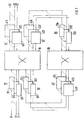
- Group 31 contains i input units 311, 312, ..., 31i; the Group 32 contains j input units 321, 322, ..., 32j; group 33 contains k input units 331, 332, ..., 33k; group 41 contains 1 output units 411, 412, ..., 41l; group 42 contains k output units 421, 422, ..., 42k; group 43 contains j output units 431, 432, ..., 43j.
- Each of the inputs I1, I2, ..., Ii of the exchange is connected to the input of one of the input units 311, 312, ..., 31i connected to group 31, the outputs of each are connected to an input of the main switching matrix 10.
- Each of the outputs O1, O2, ..., Ol of the exchange is connected to the output of one of the output units 411, 412, ..., 41l of group 41 connected, the inputs of each are connected to an output of the switching matrix 10.
- the inputs of the output units 421, 422, ..., 42k of the Group 42 are with further outputs of the Main switching matrix 10 connected.
- the outputs of the Output units 421, 422, ..., 42k of group 42 are each with the input of one of the input units 331, 332, ..., 33k connected to group 33, the outputs of which Inputs of the switching matrix 20 are connected.
- the inputs of the output units 431, 432, ..., 43j the Group 43 are each with an output of the copy switching matrix 20 connected.
- the outputs of the output units 431, 432, ..., 43j of group 43 are each with the entrance one of the input units 321, 322, ..., 32j of the group 32 connected, the outputs of which are connected to further inputs of the Main switching matrix 10 are connected.
- the main switching matrix 10 contains a plurality of in coupling elements arranged in several stages. It is so established that connections between each input and any exit are possible. Examples of such Coupling fields are familiar to any specialist.
- the individual coupling elements are constructed so that they switchable by information contained in the cell header are between a first type of addressing, in which the Cell due to one by means of an outside influenceable algorithm evaluated route information is forwarded, and a second type of addressing, where the cell due to the help of a Connection table evaluated route information is forwarded. It is provided that the second type of addressing a cell is also copied and opened can be forwarded in several ways.
- a RAM with M address bits and N Data bits.
- the address bits are identified by the for this coupling element valid bits of route information formed, the data bits give that output line to be spent on. Are multiple data bits set at the same time, the cell will be on several Output lines output, making it easy copying of cells is achieved.
- the coupling elements must be designed so that they are on can work in two different ways. For this is basically a structure suitable, as it is based on the Figures 3 and 5 of DE-A1 37 42 939.6 is described.
- the partial coupling elements 22 and 24 described there must be replaced here by a partial coupling element for the first type of addressing and a partial coupling element for the second type of addressing.
- the main switching matrix 10 is for Point-to-point connections optimized. This is how it is built and operated so that in the first half each cell takes any path, so that the Traffic is divided equally. In the second Half each cell is then targeted to the desired one Exit directed. Each middle stage coupling element must therefore from every input of the main switching matrix be reachable and also every exit of the Main switching matrix can reach.
- a reversing switching matrix is preferred as the main switching matrix.
- Each coupling element of the first stage is included at the same time coupling element of the last stage.
- a part its inputs are with inputs of the main switching matrix, another part of its inputs is with outputs from Coupling elements of the penultimate coupling stage connected.
- a Part of its outputs is with inputs from Coupling elements of the second coupling stage connected other part of its outputs is with outputs of the Main switching matrix connected.
- Each coupling element of the second stage is also the coupling element of the penultimate step, etc. The number of steps is odd.
- Such switching matrixes are from Time division multiplex technology known, for example from the mentioned article "SYSTEM 12, digital switching network". she have the advantage that the middle levels are not must be used for every connection.
- the copy switching matrix 20 can be made of the same Coupling elements can be constructed, but here only one the types of addressing is used. In contrast to Main switching matrix 10 does not have to be every output of be reachable at every entrance. It is enough if by everyone Input from a given number of outputs is achievable. It doesn't have to be from everyone Input can be reached from the same number of outputs.
- the copy switching matrix 20 can therefore consist of one part consist of 128 outputs from each input are reachable and from another part, in which of each input can be reached from 32 outputs. It must of course, take into account that the whole Traffic load from the entrance of the copy switching matrix to its output depending on the average Copy factor increases.
- ATM switch will only be added Input unit needed if the coming from outside Cells do not already have a sequence Brand contains or if this is not readily is usable.
- the basic idea of this embodiment is stop each cell at the exit until it is ensured that no older cell is on the move can be cached. Before sharing the The cell is checked to see if it is later at the exit arrived cells is still a cell that was previously is to be spent.
- This is preferably realized in that on the output side there is a buffer memory which is operated at least partially like a shift register and thereby causes a predetermined delay.
- the output of a cell will be at least the part of the buffer memory operated in the form of a shift register then examined whether a later enrolled Cell to be output earlier. If so, the two will Cells swapped.
- an output unit is used assume a data stream that is on cell width is parallelized, in which all bits of a cell passed on simultaneously on parallel lines will. As a rule, this is neither given nor particularly advantageous.
- the present Embodiment to a specific predetermined Data format, such as the one inside ATM switch is used to adapt.
- a specific predetermined Data format such as the one inside ATM switch is used to adapt.
- Dealing with indirect addressing is common for every specialist. In the example shown, it can also be used easily are used, where instead of the data the address is saved under which the data are actually saved.
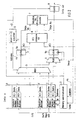
- the output unit shown in FIG. 2 has one Buffer memory 1, a memory management unit 2, two Multiplexers 3 and 4, two buffers 5a and 5b, two comparators 6 and 7, another buffer 8 and a counter 9 on.
- VCI The second type, identifies the Belonging a cell to a certain virtual Connection.
- Data, 1 instead of the rest of the cell, Data, 1 also the address under which this is saved Rest is stored in another memory.
- the buffer memory 1 is divided into three parts, namely a shift register-like part, Shift Register, with memory locations 1 to d and one after Kind of a FIFO memory operated part, FIFO, the again from two parts with memory locations d + 1 to r and r + 1 to p is composed. At least on that Storage locations 1 to r must be individually such can be accessed so that their contents are read can or that new content is written into it can be.
- the dimensioning of the buffer memory i.e. the vote the numerical values for d, r and p must be specific Use case. This must be taken into account above all the permissible error rate, the minimum and maximum runtime of a cell since the first Branch point, the number of simultaneously over one Connections approved for an output unit Connection allowed minimum and maximum number of Cells per unit of time and their permitted Fluctuation range.
- d 10
- Point-to-multipoint connections initially the Main switch 10, then the copy switch 20 and then run through the main switching matrix 10 again, are the above values with a factor of 2 ...
- Cells arriving at the input of the output unit are first examined to see if it is at the exit cells to be output or those that are in the Output unit ends. On the one hand, these are empty cells, on the other hand, the control signals for the Output unit (or one usually associated with it) Input unit that cannot be reached otherwise) contain.
- the cells to be output are in the Buffer memory 1 entered such that they first in that operated in the manner of a FIFO memory Part down to the lowest free space "fall through”. Whenever there is a cell at the exit is output, all cells move in the buffer memory one space down. Is the last Memory space of the FIFO memory, d + 1, is used, then the cell it contains in the first memory location of the shift register, d.
- the memory management unit 2 is only very much in FIG. 2 shown schematically.
- the first task is the normal operation of the To ensure buffer memory 1. This is done by Creation of addresses, address, write commands, W, and Read commands, R. Also, in Fig. 2 is not shown, information about the presence or Absence of a cell to be enrolled required.
- the memory management unit 2 also has the task of the content of the addressed by the counter 9 Storage space, address, against the content of the To exchange buffer memory 5b if a command to do this Swap is given.
- the multiplexer 3 can optionally on the content one of the memory locations 2 to r of the buffer memory 1 accessed and passed on to the buffer 5a will.
- the storage location is selected by the Counter 9, Address.
- swap is by means of of the multiplexer 4 the content of the buffer memory 5a in the buffer 5b taken over. That by means of the same Command, swap, written in the buffer memory 5b and reading from it is nothing unusual and can be carried out by a specialist using customary measures be taken into account.
- the comparator 6 marks the second type, VCI, compared to those two cells that just stored in the buffers 5a and 5b are. Only if the two brands of the second kind are identical, i.e. if the two cells of the same connection the following comparator is activated.
- the comparator 7 compares the brands of the first kind, Sequence Number, the two in the buffers 5a and 5b contained cells. If comparator 6 shows that both cells belong to the same connection and will found that the contained in the buffer 5a Cell is older than that in buffer 5b a command, swap, is issued by which the older cell in the buffer 5b and the younger cell in its place in the buffer memory 1 be taken over. As a result, the two Cells swapped.
- the content of the Buffer 5b which in the previous cycle as the oldest cell belonging to a particular connection was recognized, is transferred to the buffer 8 and is available for output at its exit, Cells out Available.
- the content of the Storage location 1 of the buffer memory 1 via the Multiplexer 4 taken over in the buffer memory 5b. Then the storage locations 2 down to r on older cells (brands of the first kind) Connection (brands of the second kind) examined.
- the representation of the output unit selected in FIG. 2 shows above all how the output unit works.
- the construction and management of the buffer memory with a part operated in the manner of a FIFO memory and a part operated like a shift register clearly in the illustration chosen in FIG Expression.
- the distribution of clocks, including the Write and read commands are not shown here.
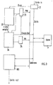
- the buffer memory is a read-write memory (RAM), 1 ', realized.
- the incoming cells are over an input memory 21 on a data bus, data, given on which the read-write memory 1 ' connected.
- a registration control 22 is from Input memory 21 activated, busy if one cell to be registered. Via the registered counter 23 becomes an address PW via an address bus, Address read-write memory 1 'and the cell in registered this. Then the Registration counter 23 from the registration controller 22 incremented.
- a readout control 24 outputs a Read counter 25 the address, PR, to which the Storage space 1 corresponds. After each issue of a Cell is the readout counter 25 from the readout control 24 from incremented.
- the difference between the content PW of the enrollment counter 23 and the content PR of the Readout counter 25 must always be at least equal to d. This is monitored by the registration control 22 and if necessary, FIFO empty, to the readout controller 24 reported, which is then sent to the data bus, data, an empty cell, Empty Cell, creates and registered in the by the Registered counter 23 causes the specified storage space and then increment the enrollment counter 23.
- the rest of the output unit is here by one Access, comparator and output unit 100 shown.
- the part of the Buffer memory does not necessarily have to form the end of it. He can also be at the beginning or in the middle of the buffer memory lie.
- the dimensions, and thus the storage requirements, depend not only of the structure of the exchange and the predetermined permissible error rates, but also from the mode of operation.
- Typical examples of point-to-multipoint connections are conference calls and sound or Television broadcasting.
- the associated cells represent a continuous signal stream. she arise at the transmitter at constant intervals and are not only in the correct order for the recipient, but also back to the original constant Distances needed.
- the Group 42 and Group 43 output units may or may not exist for themselves. Also if already in one of groups 42 or 43 the original episode has been restored, it may make sense in the next output unit, in group 41 at the latest, again the same the result to use distinctive brands. Therefore, too group 33 and group 32 input units either be there for yourself or not. Group 33 must not be present if group 42 is not present; group 32 must not exist if group 43 does not exist.
Landscapes
- Engineering & Computer Science (AREA)
- Computer Networks & Wireless Communication (AREA)
- Signal Processing (AREA)
- Data Exchanges In Wide-Area Networks (AREA)
- Use Of Switch Circuits For Exchanges And Methods Of Control Of Multiplex Exchanges (AREA)
Claims (4)
- Commutateur MTA avec capacité de duplication, destiné à la commutation de cellules MTA, comportant respectivement un en-tête de cellule avec une information de cheminement, avec un réseau principal de commutation (10) comprenant plusieurs organes de commutation disposés sur plusieurs étages, dans lequel entre chaque entrée et chaque sortie, plusieurs communications sont possibles et dans lequel les organes de commutation sont commutables par une information contenue dans l'en-tête de cellule, entre un premier type d'adressage dans lequel l'information de cheminement est analysée sur la base d'un algorithme non influençable de l'extérieur, et un second type d'adressage dans lequel l'information de cheminement est analysée à l'aide d'un tableau de communications modifiable, dans le cas du second type d'adressage, une cellule pouvant être également dupliquée et transmise sur plusieurs voies, caractérisé en ce que respectivement une unité de sortie (111, 412, ..., 411) est disposée entre le réseau de commutation principal (10) et chaque sortie (01, 02, ..., 01) du commutateur, chaque unité de sortie comportant une mémoire tampon (1) dans laquelle sont enregistrées toutes les cellules devant être émises par l'intermédiaire de cette unité de sortie après avoir quitté le réseau de commutation principal (10) et à partir de laquelle les cellules sont émises dans un ordre qui est déterminé par un repère figurant dans l'en-tête de cellule (Sequence Number) et destiné à identifier l'ordre et en ce qu'il existe un réseau de commutation de duplication (20) qui peut être atteint à partir de chaque entrée (I1, I2, ..., Ii) du commutateur dans laquelle pour chaque cellule, est réalisé un nombre déterminé de duplications qui quittent le réseau de commutation de duplication (20) à des sorties différentes, les sorties de ce réseau étant reliées aux entrées du réseau de commutation principal (10).
- Commutateur selon la revendication 1, caractérisé en ce que les entrées (l1, ..., li) du commutateur sont reliées au réseau de commutation de duplication (20) par l'intermédiaire du réseau de commutation principal (10).
- Commutateur selon la revendication 1, caractérisé en ce qu'une unité de sortie (431, ..., 43j) est respectivement insérée entre les sorties du réseau de commutation de duplication (20) et les entrées du réseau de commutation principal (10).
- Commutateur selon la revendication 1, caractérisé en ce que, entre chaque entrée (I1, ..., Ii) du commutateur et le réseau principal de commutation (10), il est prévu une unité d'entrée (311 ..., 31i) dans laquelle chaque cellule est associée à un repère (Sequence Number) permettant d'identifier l'ordre.
Applications Claiming Priority (2)
| Application Number | Priority Date | Filing Date | Title |
|---|---|---|---|
| DE4008078A DE4008078A1 (de) | 1990-03-14 | 1990-03-14 | Kopierfaehige atm-vermittlungsstelle |
| DE4008078 | 1990-03-14 |
Publications (3)
| Publication Number | Publication Date |
|---|---|
| EP0446589A2 EP0446589A2 (fr) | 1991-09-18 |
| EP0446589A3 EP0446589A3 (en) | 1992-09-02 |
| EP0446589B1 true EP0446589B1 (fr) | 1998-12-23 |
Family
ID=6402145
Family Applications (1)
| Application Number | Title | Priority Date | Filing Date |
|---|---|---|---|
| EP91101099A Expired - Lifetime EP0446589B1 (fr) | 1990-03-14 | 1991-01-29 | Commutateur ATM avec capacité de duplication |
Country Status (9)
| Country | Link |
|---|---|
| US (1) | US5202885A (fr) |
| EP (1) | EP0446589B1 (fr) |
| JP (1) | JP2986238B2 (fr) |
| KR (1) | KR0142179B1 (fr) |
| AT (1) | ATE175064T1 (fr) |
| AU (1) | AU631051B2 (fr) |
| CA (1) | CA2038121C (fr) |
| DE (2) | DE4008078A1 (fr) |
| ES (1) | ES2127719T3 (fr) |
Families Citing this family (40)
| Publication number | Priority date | Publication date | Assignee | Title |
|---|---|---|---|---|
| EP0447769A3 (en) * | 1990-03-12 | 1994-12-21 | Sel Alcatel Ag | Method and circuit arrangement for managing uniform unities and switching element |
| JP2993715B2 (ja) * | 1990-08-17 | 1999-12-27 | 株式会社日立製作所 | Atmスイッチおよびその制御方法 |
| AU641828B2 (en) * | 1990-11-27 | 1993-09-30 | Telstra Corporation Limited | A method of transmitting data on a telecommunications network |
| CA2098110A1 (fr) * | 1990-12-12 | 1992-06-12 | Gary J. Anido | Etablissement de destinations multiples dans un commutateur de paquets |
| US6411620B1 (en) * | 1991-01-31 | 2002-06-25 | Fujitsu Limited | Connectionless communication system |
| AU661988B2 (en) * | 1991-01-31 | 1995-08-17 | Fujitsu Limited | Connectionless communication system |
| US5809012A (en) * | 1991-01-31 | 1998-09-15 | Fujitsu Limited | Connectionless communication system |
| GB2258366B (en) * | 1991-08-02 | 1995-03-29 | Plessey Telecomm | An ATM switching arrangement |
| DE69132536T2 (de) * | 1991-08-21 | 2001-10-04 | International Business Machines Corp., Armonk | Verbindungslose ATM-Datendienste |
| EP0537382A1 (fr) * | 1991-10-15 | 1993-04-21 | ALCATEL BELL Naamloze Vennootschap | Arrangement et procédé pour contrôler de transfert des paquets |
| US5383181A (en) * | 1991-10-31 | 1995-01-17 | Nec Corporation | Packet switching system capable of reducing a delay time for each packet |
| EP0794683B1 (fr) * | 1991-11-29 | 2004-03-31 | Nec Corporation | Système de commutation ATM optique à auto-acheminement avec réseau de réplication optique |
| US5444702A (en) * | 1992-09-14 | 1995-08-22 | Network Equipment Technologies, Inc. | Virtual network using asynchronous transfer mode |
| JP3104429B2 (ja) * | 1992-10-08 | 2000-10-30 | 株式会社日立製作所 | コピー機能を有する共通バッファ形atmスイッチ及びそのコピー方法 |
| GB2273224B (en) * | 1992-12-05 | 1997-01-22 | Netcomm Ltd | An ATM Cell switch suitable for multicast switching |
| DE4308174C1 (de) * | 1993-03-15 | 1994-03-24 | Siemens Ag | Verfahren für Punkt-zu-Mehrpunkt-Verbindungen in selbstroutenden ATM-Koppelfeldern |
| ES2148197T3 (es) * | 1993-06-29 | 2000-10-16 | Cit Alcatel | Metodo de resecuenciacion y dispositivo de resecuenciacion que realiza tal metodo. |
| EP0641106A1 (fr) * | 1993-08-27 | 1995-03-01 | Siemens Aktiengesellschaft | Système de commutation à ATM |
| DE4330295C2 (de) * | 1993-09-07 | 1995-12-07 | Siemens Ag | Verfahren und Koppelfeldanordnung zum Übertragen von Zellen im Zuge einer Punkt-zu-Mehrpunktverbindung in einer Paketvermittlungsanlage |
| US5636210A (en) * | 1995-08-02 | 1997-06-03 | Agrawal; Jagannath P. | Asynchronous transfer mode packet switch |
| JPH0955749A (ja) * | 1995-08-14 | 1997-02-25 | Fujitsu Ltd | セル交換機におけるルート選択方法 |
| JP3851660B2 (ja) * | 1995-09-06 | 2006-11-29 | 富士通株式会社 | 通信サービス制御用交換装置 |
| US6016319A (en) * | 1995-10-31 | 2000-01-18 | Lucent Technologies, Inc. | Communications system for transmission of datagram packets over connection-oriented networks |
| KR100278016B1 (ko) * | 1995-12-26 | 2001-01-15 | 윤종용 | 비동기 전송모드 교환시스템의 스위칭 장치 및 방법 |
| US5793764A (en) * | 1996-03-12 | 1998-08-11 | International Business Machines Corporation | LAN switch with distributed copy function |
| US5909438A (en) * | 1996-09-18 | 1999-06-01 | Cascade Communications Corp. | Logical multicast from a switch configured for spatial multicast |
| SE511957C2 (sv) * | 1996-12-06 | 1999-12-20 | Ericsson Telefon Ab L M | Broadcasting över ATM |
| KR100467708B1 (ko) | 1996-12-21 | 2005-05-11 | 삼성전자주식회사 | 비동기전송모드교환시스템의셀처리장치및방법 |
| NO970467L (no) | 1997-02-03 | 1998-08-04 | Ericsson Telefon Ab L M | FremgangsmÕte for Õ regenerere et punkt-til-multipunkt grensesnitt pÕ et punkt-til-punkt grensesnitt |
| JPH11154954A (ja) | 1997-11-20 | 1999-06-08 | Hitachi Ltd | Atmスイッチ |
| US6693904B1 (en) * | 1998-04-09 | 2004-02-17 | Lucent Technologies Inc. | Trace format for a sliced switch fabric |
| US6320864B1 (en) | 1998-06-19 | 2001-11-20 | Ascend Communications, Inc. | Logical multicasting method and apparatus |
| JP3537318B2 (ja) | 1998-07-24 | 2004-06-14 | 富士通株式会社 | 特定のコネクションの通信データを加工する交換機および交換方法 |
| US6760332B1 (en) * | 1999-06-03 | 2004-07-06 | Fujitsu Network Communications, Inc. | ATM multicasting system and method |
| KR100307926B1 (ko) * | 1999-08-04 | 2001-09-29 | 서평원 | 멀티캐스트 서비스가 가능한 공유 메모리형 에이티엠 스위치 |
| KR100465428B1 (ko) * | 2000-12-28 | 2005-01-13 | 엘지전자 주식회사 | 이동 전화 교환 시스템의 톤 자원 관리 방법 |
| US7233576B1 (en) | 2001-08-16 | 2007-06-19 | Network General Technology | Method and apparatus for transferring data from an ATM connection table to memory for use by an application program |
| US20030214949A1 (en) * | 2002-05-16 | 2003-11-20 | Nadim Shaikli | System for reordering sequenced based packets in a switching network |
| KR100893045B1 (ko) * | 2002-06-27 | 2009-04-15 | 주식회사 케이티 | 비동기전송모드 망에서 점대다중점 연결을 이용한 방송서비스 제공 시스템 및 그 방법 |
| JP6003862B2 (ja) * | 2013-09-30 | 2016-10-05 | ヤマハ株式会社 | ポート制御方法、ミキサシステム、及び、プログラム |
Family Cites Families (11)
| Publication number | Priority date | Publication date | Assignee | Title |
|---|---|---|---|---|
| JPS55140347A (en) * | 1979-04-20 | 1980-11-01 | Oki Electric Ind Co Ltd | Information sequence security system |
| US4700184A (en) * | 1981-10-15 | 1987-10-13 | L'etat Francais | One-way data packet transmission system for processing data arranged in groups |
| US4701906A (en) * | 1985-06-27 | 1987-10-20 | American Telephone And Telegraph Company, At&T Bell Laboratories | Packet switching network with multiple packet destinations |
| US4700344A (en) * | 1986-06-13 | 1987-10-13 | Ncr Corporation | Processor overrun circuit |
| JPS63246055A (ja) * | 1987-03-31 | 1988-10-13 | Nec Corp | パケツト送受信装置 |
| US4983962A (en) * | 1987-09-14 | 1991-01-08 | Hammerstrom Daniel W | Neural-model, computational architecture employing broadcast hierarchy and hypergrid, point-to-point communication |
| DE3742939A1 (de) * | 1987-12-18 | 1989-07-06 | Standard Elektrik Lorenz Ag | Verfahren zur hybriden paketvermittlung und einrichtungen hierzu |
| DE3816747A1 (de) * | 1988-05-17 | 1989-11-30 | Standard Elektrik Lorenz Ag | Leistungsvermittelnde paket-vermittlungseinrichtung |
| DE68929523T2 (de) * | 1988-07-22 | 2005-12-15 | Hitachi, Ltd. | ATM-Vermittlungssystem |
| JP2964151B2 (ja) * | 1989-07-03 | 1999-10-18 | 富士通株式会社 | 通信制御方式 |
| US4991171A (en) * | 1989-09-26 | 1991-02-05 | At&T Bell Laboratories | Broadcast packet switch network |
-
1990
- 1990-03-14 DE DE4008078A patent/DE4008078A1/de not_active Withdrawn
-
1991
- 1991-01-29 ES ES91101099T patent/ES2127719T3/es not_active Expired - Lifetime
- 1991-01-29 EP EP91101099A patent/EP0446589B1/fr not_active Expired - Lifetime
- 1991-01-29 DE DE59109079T patent/DE59109079D1/de not_active Expired - Fee Related
- 1991-01-29 AT AT91101099T patent/ATE175064T1/de not_active IP Right Cessation
- 1991-03-12 AU AU72835/91A patent/AU631051B2/en not_active Ceased
- 1991-03-12 CA CA002038121A patent/CA2038121C/fr not_active Expired - Fee Related
- 1991-03-12 US US07/668,160 patent/US5202885A/en not_active Expired - Fee Related
- 1991-03-13 KR KR1019910003969A patent/KR0142179B1/ko not_active IP Right Cessation
- 1991-03-14 JP JP7468791A patent/JP2986238B2/ja not_active Expired - Lifetime
Also Published As
| Publication number | Publication date |
|---|---|
| DE59109079D1 (de) | 1999-02-04 |
| EP0446589A3 (en) | 1992-09-02 |
| ES2127719T3 (es) | 1999-05-01 |
| AU7283591A (en) | 1991-09-19 |
| AU631051B2 (en) | 1992-11-12 |
| EP0446589A2 (fr) | 1991-09-18 |
| JPH07321793A (ja) | 1995-12-08 |
| DE4008078A1 (de) | 1991-09-19 |
| JP2986238B2 (ja) | 1999-12-06 |
| CA2038121A1 (fr) | 1991-09-15 |
| US5202885A (en) | 1993-04-13 |
| ATE175064T1 (de) | 1999-01-15 |
| CA2038121C (fr) | 1994-05-31 |
| KR910017902A (ko) | 1991-11-05 |
| KR0142179B1 (ko) | 1998-08-17 |
Similar Documents
| Publication | Publication Date | Title |
|---|---|---|
| EP0446589B1 (fr) | Commutateur ATM avec capacité de duplication | |
| EP0435046B1 (fr) | Méthode pour le rétablissement de la séquence des cellules originelles, notamment pour un commutateur ATM, ainsi qu'unité de sortie pour celui-ci | |
| EP0320772B1 (fr) | Procédé pour la commutation hybride de paquets et dispositifs à cet effet | |
| DE69124645T2 (de) | Verfahren und Schaltung zur Verkehrsformung | |
| DE69637462T2 (de) | ATM-Vermittlungsstelle mit Eingangs- und Ausgangsanschlussstellen | |
| DE3742941C2 (fr) | ||
| DE3752370T2 (de) | Vermittlungssystem | |
| DE3856510T2 (de) | Mehrstufige Vermittlungseinrichtung für Nachrichtenkanäle | |
| EP0446586B1 (fr) | Central de commutation ATM | |
| DE3875993T2 (de) | Vermittlungssystem fuer hybride zeitmultiplexe. | |
| DE3787600T2 (de) | Koppelpunktschaltung für Datenpaketraumvermittlung. | |
| EP0412343A2 (fr) | Réseau de commutation et module pour un système ATM | |
| EP0351014B1 (fr) | Réseau de commutation pour système de commutation | |
| EP0004307B1 (fr) | Procédé pour la réalisation de connexions en conférence dans un système de commutation temporelle MIC | |
| CH653783A5 (de) | Steuereinrichtung, insbesondere fuer fernsprechvermittlungsanlagen. | |
| DE69112490T2 (de) | Mehrweg- und Selbstlenkungsvermittlungsnetz zur Vermittlung von asynchronen Zeitmultiplexeinheiten mit Verfügbarkeitszeichen. | |
| DE2822896C2 (fr) | ||
| EP0428089B1 (fr) | Noeud d'abonné d'un système de transmission de données numérique | |
| DE1934097C3 (de) | Verbindungsnetz großer Kapazität für Vermittlungsanlagen vom Typ PCM-Zeitmultiplex | |
| EP0322075B1 (fr) | Réseau de commutation et dispositif de commande pour un système de commutation | |
| EP0447769A2 (fr) | Méthode et dispositif de gestion d'unité uniformes et élément de commutation | |
| EP0173274B1 (fr) | Méthode et montage pour la réalisation et la maintenance d'une liaison à division temporelle à large bande | |
| DE19911830A1 (de) | Verfahren zum Verwalten des Zugriffs auf einen Bus und Bussystem | |
| DE69415278T2 (de) | Anordnung für Warteschlangen zur Verwendung in der Eingangsstufe einer nicht blockierenden Raumschaltmatrix | |
| EP0685949A2 (fr) | Système de transmission de paquets |
Legal Events
| Date | Code | Title | Description |
|---|---|---|---|
| PUAI | Public reference made under article 153(3) epc to a published international application that has entered the european phase |
Free format text: ORIGINAL CODE: 0009012 |
|
| AK | Designated contracting states |
Kind code of ref document: A2 Designated state(s): AT BE CH DE ES FR GB IT LI NL SE |
|
| PUAL | Search report despatched |
Free format text: ORIGINAL CODE: 0009013 |
|
| AK | Designated contracting states |
Kind code of ref document: A3 Designated state(s): AT BE CH DE ES FR GB IT LI NL SE |
|
| 17P | Request for examination filed |
Effective date: 19920915 |
|
| RAP3 | Party data changed (applicant data changed or rights of an application transferred) |
Owner name: ALCATEL N.V. Owner name: ALCATEL SEL AKTIENGESELLSCHAFT |
|
| 17Q | First examination report despatched |
Effective date: 19940817 |
|
| GRAG | Despatch of communication of intention to grant |
Free format text: ORIGINAL CODE: EPIDOS AGRA |
|
| GRAG | Despatch of communication of intention to grant |
Free format text: ORIGINAL CODE: EPIDOS AGRA |
|
| GRAH | Despatch of communication of intention to grant a patent |
Free format text: ORIGINAL CODE: EPIDOS IGRA |
|
| GRAH | Despatch of communication of intention to grant a patent |
Free format text: ORIGINAL CODE: EPIDOS IGRA |
|
| RAP1 | Party data changed (applicant data changed or rights of an application transferred) |
Owner name: ALCATEL ALSTHOM COMPAGNIE GENERALE D'ELECTRICITE |
|
| GRAA | (expected) grant |
Free format text: ORIGINAL CODE: 0009210 |
|
| RAP1 | Party data changed (applicant data changed or rights of an application transferred) |
Owner name: ALCATEL ALSTHOM COMPAGNIE GENERALE D'ELECTRICITE |
|
| AK | Designated contracting states |
Kind code of ref document: B1 Designated state(s): AT BE CH DE ES FR GB IT LI NL SE |
|
| REF | Corresponds to: |
Ref document number: 175064 Country of ref document: AT Date of ref document: 19990115 Kind code of ref document: T |
|
| REG | Reference to a national code |
Ref country code: CH Ref legal event code: EP |
|
| RAP2 | Party data changed (patent owner data changed or rights of a patent transferred) |
Owner name: ALCATEL |
|
| REG | Reference to a national code |
Ref country code: CH Ref legal event code: NV Representative=s name: CABINET ROLAND NITHARDT CONSEILS EN PROPRIETE INDU |
|
| REF | Corresponds to: |
Ref document number: 59109079 Country of ref document: DE Date of ref document: 19990204 |
|
| NLT2 | Nl: modifications (of names), taken from the european patent patent bulletin |
Owner name: ALCATEL |
|
| GBT | Gb: translation of ep patent filed (gb section 77(6)(a)/1977) |
Effective date: 19990219 |
|
| ET | Fr: translation filed | ||
| REG | Reference to a national code |
Ref country code: ES Ref legal event code: FG2A Ref document number: 2127719 Country of ref document: ES Kind code of ref document: T3 |
|
| PLBE | No opposition filed within time limit |
Free format text: ORIGINAL CODE: 0009261 |
|
| STAA | Information on the status of an ep patent application or granted ep patent |
Free format text: STATUS: NO OPPOSITION FILED WITHIN TIME LIMIT |
|
| 26N | No opposition filed | ||
| PGFP | Annual fee paid to national office [announced via postgrant information from national office to epo] |
Ref country code: GB Payment date: 20011214 Year of fee payment: 12 |
|
| PGFP | Annual fee paid to national office [announced via postgrant information from national office to epo] |
Ref country code: DE Payment date: 20011217 Year of fee payment: 12 Ref country code: CH Payment date: 20011217 Year of fee payment: 12 |
|
| PGFP | Annual fee paid to national office [announced via postgrant information from national office to epo] |
Ref country code: FR Payment date: 20011226 Year of fee payment: 12 |
|
| PGFP | Annual fee paid to national office [announced via postgrant information from national office to epo] |
Ref country code: NL Payment date: 20011227 Year of fee payment: 12 |
|
| PGFP | Annual fee paid to national office [announced via postgrant information from national office to epo] |
Ref country code: AT Payment date: 20011228 Year of fee payment: 12 |
|
| REG | Reference to a national code |
Ref country code: GB Ref legal event code: IF02 |
|
| PGFP | Annual fee paid to national office [announced via postgrant information from national office to epo] |
Ref country code: SE Payment date: 20020102 Year of fee payment: 12 |
|
| PGFP | Annual fee paid to national office [announced via postgrant information from national office to epo] |
Ref country code: ES Payment date: 20020118 Year of fee payment: 12 |
|
| PGFP | Annual fee paid to national office [announced via postgrant information from national office to epo] |
Ref country code: BE Payment date: 20020220 Year of fee payment: 12 |
|
| PG25 | Lapsed in a contracting state [announced via postgrant information from national office to epo] |
Ref country code: GB Free format text: LAPSE BECAUSE OF NON-PAYMENT OF DUE FEES Effective date: 20030129 Ref country code: AT Free format text: LAPSE BECAUSE OF NON-PAYMENT OF DUE FEES Effective date: 20030129 |
|
| PG25 | Lapsed in a contracting state [announced via postgrant information from national office to epo] |
Ref country code: SE Free format text: LAPSE BECAUSE OF NON-PAYMENT OF DUE FEES Effective date: 20030130 Ref country code: ES Free format text: LAPSE BECAUSE OF NON-PAYMENT OF DUE FEES Effective date: 20030130 |
|
| PG25 | Lapsed in a contracting state [announced via postgrant information from national office to epo] |
Ref country code: LI Free format text: LAPSE BECAUSE OF NON-PAYMENT OF DUE FEES Effective date: 20030131 Ref country code: CH Free format text: LAPSE BECAUSE OF NON-PAYMENT OF DUE FEES Effective date: 20030131 Ref country code: BE Free format text: LAPSE BECAUSE OF NON-PAYMENT OF DUE FEES Effective date: 20030131 |
|
| PG25 | Lapsed in a contracting state [announced via postgrant information from national office to epo] |
Ref country code: NL Free format text: LAPSE BECAUSE OF NON-PAYMENT OF DUE FEES Effective date: 20030801 Ref country code: DE Free format text: LAPSE BECAUSE OF NON-PAYMENT OF DUE FEES Effective date: 20030801 |
|
| EUG | Se: european patent has lapsed | ||
| REG | Reference to a national code |
Ref country code: CH Ref legal event code: PL |
|
| GBPC | Gb: european patent ceased through non-payment of renewal fee | ||
| PG25 | Lapsed in a contracting state [announced via postgrant information from national office to epo] |
Ref country code: FR Free format text: LAPSE BECAUSE OF NON-PAYMENT OF DUE FEES Effective date: 20030930 |
|
| NLV4 | Nl: lapsed or anulled due to non-payment of the annual fee |
Effective date: 20030801 |
|
| REG | Reference to a national code |
Ref country code: FR Ref legal event code: ST |
|
| REG | Reference to a national code |
Ref country code: ES Ref legal event code: FD2A Effective date: 20030130 |
|
| PG25 | Lapsed in a contracting state [announced via postgrant information from national office to epo] |
Ref country code: IT Free format text: LAPSE BECAUSE OF NON-PAYMENT OF DUE FEES;WARNING: LAPSES OF ITALIAN PATENTS WITH EFFECTIVE DATE BEFORE 2007 MAY HAVE OCCURRED AT ANY TIME BEFORE 2007. THE CORRECT EFFECTIVE DATE MAY BE DIFFERENT FROM THE ONE RECORDED. Effective date: 20050129 |