EP0428089B1 - Noeud d'abonné d'un système de transmission de données numérique - Google Patents
Noeud d'abonné d'un système de transmission de données numérique Download PDFInfo
- Publication number
- EP0428089B1 EP0428089B1 EP90121572A EP90121572A EP0428089B1 EP 0428089 B1 EP0428089 B1 EP 0428089B1 EP 90121572 A EP90121572 A EP 90121572A EP 90121572 A EP90121572 A EP 90121572A EP 0428089 B1 EP0428089 B1 EP 0428089B1
- Authority
- EP
- European Patent Office
- Prior art keywords
- memory
- time
- connections
- buffer memory
- interface
- Prior art date
- Legal status (The legal status is an assumption and is not a legal conclusion. Google has not performed a legal analysis and makes no representation as to the accuracy of the status listed.)
- Expired - Lifetime
Links
Images


Classifications
-
- H—ELECTRICITY
- H04—ELECTRIC COMMUNICATION TECHNIQUE
- H04Q—SELECTING
- H04Q11/00—Selecting arrangements for multiplex systems
- H04Q11/04—Selecting arrangements for multiplex systems for time-division multiplexing
Definitions
- the invention relates to a subscriber line node of a digital message transmission system for the bidirectional transmission of message signals according to the preamble of claim 1.
- the subscriber connection node is the unit of a digital message transmission system in which the message signals, for example coming from a switching center, are prepared for the transmissions to the individual subscriber terminals, taking into account the existing network. Connections are often present on the side of the subscriber connection node facing the subscriber terminals, in which connections of a switching center are combined. If fewer channels are now required in the apron facility than are available, channels are used in the exchange in this way that are not used by any subscriber.
- An optical message transmission system is known from EP 0318331 A1, in which the message transmission between subscriber line nodes and subscribers is carried out by a TDM multiplex method in the downward direction, ie. H. from the central office to the subscribers, and an uplink TDMA multiplexing process, i. H. from the participants to the exchange.
- the z. B. from the subscribers time-division multiplexed digital signals in a subscriber connection node into otherwise prepared, directed to the exchange time-division multiplexed digital signals. This conversion takes place in the subscriber line node.
- the message transmission between the subscriber line node and the apron device takes place via glass fibers.
- An additional distribution of the time-division multiplex signals takes place outside the subscriber connection node by means of optical couplers.
- the invention is based on the object of realizing the conversion of time-division multiplex signals and their distribution in a technically less complex and more flexible manner.
- a particular advantage of the invention is that time slots are time-division multiplexed for individuals Subscriber terminals can be switched between the subscriber terminals and the switching centers in any assignment and order.
- FIG. 1 shows the exemplary embodiment of a digital optical transmission system 301 with the subscriber line node 300 according to the invention.
- the connection node 300 is framed with a chain line.
- connection node 300 facing these devices form an interface A for digital 2 Mbit / s time-division multiplex signals with a frame duration of 125 microseconds.
- an adaptation circuit 314 is provided between the digital exchange VS2, the Datex device D, the device F and the devices FV, as far as necessary, which sets the transmission bit rate of the connections adapts the desired 2 Mbit / s and if necessary, if there are analog signals, carries out an analog dialog conversion.
- These adaptation circuits 314 are known as such.
- An apron device 324 is shown on the right-hand side as representative of several apron devices. A number of common connections, of which only one common connection 311 is shown, are connected to these. The common connections 311 are connected to the apron device 324 via optical waveguides 319. A plurality of subscriber terminals 313 are in turn assigned to each community connection 311. Each apron device 324 is connected to the connection node 300 via an optical waveguide 318. The transmission bit repetition frequency on the optical fiber 318 is 12 Mbit / s net. The same applies to the apron devices, not shown, which are connected to the connection node 300, so that the Connections of the front-end devices form an interface B of the connection node 300 with a uniform transmission bit repetition frequency. The digital signals transmitted via the connections at interface B are each time-division multiplexed signals with a frame clock period of one millisecond.
- connection node 300 thus has two types of connections: a first type with 144 electrical 2 Mbit / s connections at interface A and a second type with 24 optical 12 Mbit / s connections at interface B.
- the connection node 300 makes the requirement that signals present at the connections 1 to 144 of the interface A can be switched through to the connections 1 to 24 of the interface B.
- the signals arriving at connections 1 to 144 are time-division multiplexed signals (TDM), which are composed of a number of sub-signals in time division.
- TDM time-division multiplexed signals
- TDMA time division multiplex access method
- connection node 300 now has the task of forming new time-division multiplex signals from the incoming time-division multiplex signals by combining any partial signals of the incoming time-division multiplex signals into a new time-division multiplex signal in any controllable combination and order, and this at the opposite one Output interface at one of the existing connections.
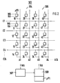
- buffers 303 which consist of a first buffer 304 (FIG. 2) and a second buffer 305 (FIG. 3).
- first buffer 304 FIG. 2
- second buffer 305 FIG. 3
- the first buffer 304 consists of a number of partial memories 11, 21, 31, 41, ...; 12, 13, 14, ..., which are arranged in a matrix in 24 rows and 24 columns. It has 24 inputs E1 to E24 and 24 outputs A1 to A24.
- the inputs of the partial memories located in each row are connected in parallel to one of the inputs E1 to E24, for example the inputs of the partial memories 11, 21, 31, 41, ... to the input E1 of the intermediate memory.
- 24 outputs A1 to A24 one is connected to the outputs of partial memories located in a column, for example A2 to the outputs of partial memories 21, 22, 23, 24, ....
- each partial memory has an input RA for read addresses and an input WA for write addresses.
- the desired possibility is created of further transmitting the partial signals within the frame from the interface B in a different order than in the order in which they occur at interface A in any frame from time-division multiplex signals arriving there.
- All signals, ie data words or partial signals of a frame, for example at input E1 are stored in each of the 24 partial memories 11, 21, 31, 41, ..., each partial signal having its own memory location (not shown), which is provided with its own read address RA and write address WA.
- the individual memory locations are designed as so-called fifo memories (first in first out), in which the data written in first are also read out first.
- the writing and reading out of the data in the buffer memory 303 takes place at the same time.
- the inputs WA for the write address of all partial memories are connected to a counter 307.
- the inputs RA for the read addresses of all partial memories are connected to a table memory 308, which is implemented as a memory of a microprocessor ⁇ P1 and is connected to the counter 307.
- the reading out of the partial memories is delayed by one frame clock period compared to the writing, since it happens that a partial signal lying behind in a frame must be read out before a partial signal lying in front of it.
- the function of the first buffer 304 which is responsible for the downward direction, is explained below.
- the frames of the incoming message signals are present at the inputs E1 to E24.
- Each partial signal of a frame is written into each partial memory, for example the partial signals of a frame arriving at E1 into the partial memories 11, 21, 31, 41, ....
- the preambles of the frames are no longer used.
- Each partial memory has a number of addressable memory locations corresponding to the number of time slots of a frame, ie partial signals of a frame.
- the storage capacity of a memory location is 8 bits, since each of the partial signals contained in a frame contains a data word from 8 Bits is.
- the read address inputs RA of all partial memories are connected to the table memory 308, which is connected to the microprocessor ⁇ P1.
- the counter 307 determines the clock in which the table memory 308 outputs the read addresses.
- the table memory 308 and the counter 307 it is possible to read any partial signal from each of the 24 input signals to each of the outputs A1 to A24, and in any order.
- a prerequisite for this is created by the memory structure described, which ensures that each output of the memory is connected to outputs of partial memories which store the partial signals of all frames received at inputs E1 to E24, so that each output has access to the entire content of all received frames Has.
- the output of a further partial memory 10, 20, 30, 40, ... is connected to each output A1 to A24, which contains several addressable memory locations and, like the other partial memories 11, 12 , 13, 14, ... has a write address input WA connected to the counter 307 and a read address input RA connected to the memory 308 and receives its data for forming the preambles from a microprocessor ⁇ P0.
- FIG. 3 shows the second buffer memory 305 which is responsible for the message transmission in the upward direction.
- the first buffer 304 has 24 signal inputs E1 to E24 and 24 signal outputs A1 to A24, each of which is connected in parallel to 24 sub-memories arranged in a column or row and arranged in a matrix.
- the inputs E1 to E24 are connected to the inputs of the partial memories and the outputs A1 to A24 to the outputs of the partial memories.
- the mode of operation of the partial memories forming the matrix-like arrangement corresponds to that from the description of the first part 304 (FIG. 2).
- the main difference lies in the arrangement of the additional partial memories 10, 20, 30, 40, the inputs of which are each connected to the inputs E1 to E24.
- the additional partial memories 10, 20, 30, 40, ... are connected to the intermediate memory 305 for receiving the preambles from the inputs E1 to E24 and for forwarding the preambles to a microprocessor ⁇ PA1, ⁇ PA2, ... connected to their output .
- microprocessors ⁇ PA1, ⁇ PA2 ... in conjunction with a central microprocessor ⁇ P0 are used to evaluate the received TDMA frame and the received TDMA preamble and the formation of the TDM frame and the TDM preamble for the others transmission in upward direction.
- the frames of the TDM signals which are to be transmitted by the connection node 300 in the upward direction are formed with the aid of partial memories 251, 252, 253, 254, ..., the outputs of which are connected to the outputs A1 to A24 of the intermediate memory 305 and the inputs of which the central microprocessor ⁇ P0 are connected.
- network management 320 The interaction of the individual microprocessors ⁇ P0, ⁇ P1, ⁇ P2, ⁇ PA1, ⁇ PA2, ... in connection with a unit controlling the entire digital message transmission system, which is referred to here as network management 320, is shown below. It is assumed that the network management 320 the cheapest connection options between the ports of interface A and those of interface B based on its information about the assignment of connections 1 to 144 of interface A, the assignment of the associated devices VS1, VS2, D, F and FV, the assignment of connections 1 to 24 of interface B, the assignment of the associated front-end devices 324, the type and number of the community connections 311 connected to them and their assignment.
- the network management 320 is able to determine the most favorable connection between the connections 1 to 144 of the interface A and the connections 1 to 24 of the interface B, whereby efforts are made to make the connections 1 to 144 of the interface A as full as possible to prove what is particularly necessary when individual connections 1 to 24 at interface B are not fully occupied. This can occur if an apron device 324 is set up in a sparsely populated area with only a few participants.
- the network management 320 communicates the cheapest connection via the microprocessor ⁇ P0 to the microprocessor ⁇ P1 for the transmission in the downward direction and the microprocessor ⁇ P2 for the transmission in the upward direction.
- the transmission paths in the upward and downward direction do not have to be, but can be the same.
- the network management 320 also knows the position of the time slots for a subscriber in the frame during the transmission in upward and downward direction at both interfaces A and B, accordingly it tells the microprocessors ⁇ P1 and ⁇ P2 via the microprocessor ⁇ P0 in what order partial signals for the Formation of the corresponding frame must be read from the buffer.
- the network management 320 also knows the structures of the individual frames. It tells the microprocessor ⁇ P0 which structure the frame to be transmitted in the upward direction has at the interface B. It also tells the microprocessor ⁇ P1 which structure the frame to be transmitted in the downward direction has at the interface A.
- the microprocessors ⁇ PA1, ⁇ PA2, ... each receive their information from the preamble of the message signals arriving at the interface B in the upward direction, which e.g. May contain information about the access of a new subscriber.
- the microprocessors ⁇ PA1, ⁇ PA2, ... communicate their information to the central microprocessor ⁇ P0, which incorporates this information into the formation of the preamble of the individual frames and, if necessary, also, e.g. notifies network management 320 if a subscriber joins or drops.
- Interface A of subscriber line node 300 has 144 electrical connections with a transmission bit repetition rate of 2 Mbit / s, interface B, however, 24 optical connections with a transmission bit repetition frequency of 12 Mbit / s.
- the adaptation takes place on the one hand via multiplexer / demultiplexer 309, each of which has six connections with a transmission bit repetition frequency of 2 Combine Mbit / s into one connection with a transmission bit repetition rate of 12 Mbit / s.
- Each of the 12 Mbit / s connections of a multiplexer / demultiplexer is connected to one of the inputs E1 to E24 of the first buffer 304 or to one of the outputs A1 to A24 of the second buffer 305.
- Interface A corresponds to interface G.703 of the CCITT recommendations.
- the recommendation specifies an integer multiple of 64 kbit / s as the transmission bit rate.
- the inputs E1 to E24 of the second buffer memory 305 and the outputs A1 to A24 of the first buffer memory 304 are each connected to a multiplexer / demultiplexer 322, which converts the "net" transmission bit repetition frequency of 12 Mbit / s to a higher transmission bit repetition frequency or converts a lower transmission bit rate since the effective transmission bit rate between the node 300 and the common ports 311 due to the protection times between the data bundles associated with the TDM / TDMA system and the type of transmission method used here, which alternates periodically downwards - and upward direction is transmitted, is higher than 12 Mbit / s and is approximately 30 Mbit / s.
- Electrical-optical converters 323 are arranged between the multiplexers / demultiplexers 322 and the optical connections 1 to 24 of the interface B.
- Each connection between the intermediate memories 303 and a multiplexer 322 is connected to one of the microprocessors ⁇ PA1, ⁇ PA2, ...
- the microprocessors ⁇ PA1, ⁇ PA2, ... are connected in parallel to the central microprocessor ⁇ P0.
- the microprocessor ⁇ P0 is connected to the intermediate memories 303, the microprocessors uP1 and uP2 and the network management 320.
- connection node 300 is, in a slightly modified manner, not only for a message transmission system 301, but if, instead of the electrical-optical converter 323, a transmitting and receiving device for a microwave or satellite transmission system is arranged and corresponding base units and relay stations or satellites are present on the subscriber side are also applicable to such communication systems. Furthermore, the message signals can be transmitted between the connection nodes and the participants via electrical lines.
- the invention can also be used in connection nodes in which there is no conversion of the transmission bit rate or no electrical-optical conversion between the two interfaces A and B.
- a broadband signal coupled to the optical waveguide 318 via a fiber coupling can additionally be transmitted to the subscribers 313.
- a message signal with a higher transmission bit rate e.g. a broadband signal with a transmission bit repetition frequency of 140 Mbit / s is present.
- TDM / TDMA Time Division Multiplex
- a bidirectional TDM system can be used instead of the TDM / TDMA system.
Landscapes
- Engineering & Computer Science (AREA)
- Computer Networks & Wireless Communication (AREA)
- Time-Division Multiplex Systems (AREA)
- Data Exchanges In Wide-Area Networks (AREA)
- Communication Control (AREA)
- Small-Scale Networks (AREA)
- Mobile Radio Communication Systems (AREA)
- Optical Communication System (AREA)
Claims (6)
- Noeud de raccordement d'abonné d'un système numérique de transmission d'informations destiné à la transmission bidirectionnelle de signaux numériques de multiplexage temporel entre des premiers équipements, en particulier des centraux téléphoniques, et des deuxièmes équipements, en particulier des équipements de champs préliminaires,- dans lequel des raccordements d'un premier type forment une première interface bidirectionnelle pour des signaux numériques de multiplexage temporel d'un débit binaire de transmission prédéterminé,- dans lequel des raccordements d'un deuxième type forment une deuxième interface bidirectionnelle pour des signaux numériques de multiplexage temporel d'un débit binaire de transmission prédéterminé,- dans lequel sont disposés des multiplexeur/démultiplexeur,caractérisé en ce que- il présente une mémoire temporaire (303) avec laquelle des voies de signaux numériques de multiplexage temporel entrant à des raccordements quelconques du premier type peuvent être commutées dans un ordre quelconque en des signaux numériques de multiplexage temporel sortant à des raccordements quelconques du deuxième type et inversement,- les multiplexeur/démultiplexeur (309) sont disposés entre les raccordements du premier type et la mémoire temporaire (303),- il présente une unité de calcul (µP0) reliée à la mémoire temporaire (303) et une unité de commande (320) du système de transmission d'informations,- l'unité de calcul (µP0) de l'unité de commande (320) reçoit des informations sur la manière dont les voies de la mémoire temporaire (303) doivent être commutées. et- l'unité de calcul commande la mémoire temporaire (303) sur la base de ces informations, de manière à commuter les voies en fonction de ces informations.
- Noeud de raccordement d'abonné suivant la revendication 1, caractérisé en ce que- les mémoires temporaires (304, 305) sont constituées par une première mémoire temporaire (304) utilisée pour la transmission dans un sens, et une deuxième mémoire temporaire (305) utilisée pour la transmission dans l'autre sens, comportant chacune plusieurs mémoires partielles (11, 21, 31, 41, ..., 12, 13, 14, ...) disposées sous forme de matrice en lignes et colonnes, chacune desdites mémoires partielles comportant un certain nombre d'emplacements de mémoire adressables, et- les mémoires partielles (11, 21, 31, 41, ...) d'une ligne comportent des entrées qui sont raccordées en parallèle à une entrée (E1, ..., E24) de la mémoire temporaire, et les mémoires partielles (11, 12, 13, 14, ...) d'une colonne comportent des sorties qui sont reliées en parallèle à une sortie (A1, ..., A24) de la mémoire temporaire, ou inversement.
- Noeud de raccordement d'abonné suivant la revendication 2, caractérisé en ce qu'à la mémoire temporaire (304, 305) sont associées d'autres mémoires partielles (10, 20, 30, 40 ...; 251, 252, 253, ...) comportant des emplacements de mémoire adressables pour former des préambules et pour lire les préambules.
- Noeud de raccordement d'abonne suivant la revendication 2, caractérisé en ce que le nombre d'emplacements adressables d'une mémoire partielle (11, 21, 31, 41, ...; 10, 20, 30. 40, ...) est identique au nombre des créneaux temporels de la trame des signaux numériques de multiplexage temporel à transmettre, et en ce que la grandeur d'un emplacement de mémoire correspond au contenu de données d'un créneau temporel.
- Noeud de raccordement d'abonné suivant la revendication 4, caractérisé en ce que l'écriture du contenu d'un créneau temporel dans l'un des emplacements de mémoire d'une mémoire partielle est commandée par un compteur (307), et la lecture est commandée par une mémoire en tableau (308) reliée au compteur (307).
- Noeud de raccordement d'abonné suivant la revendication 5, caractérisé en ce que la mémoire en tableau (308) est la mémoire (308) d'un microprocesseur (µP1, µP2).
Applications Claiming Priority (2)
| Application Number | Priority Date | Filing Date | Title |
|---|---|---|---|
| DE3937738 | 1989-11-13 | ||
| DE3937738A DE3937738A1 (de) | 1989-11-13 | 1989-11-13 | Teilnehmeranschlussknoten eines digitalen nachrichtenuebertragungssystems |
Publications (3)
| Publication Number | Publication Date |
|---|---|
| EP0428089A2 EP0428089A2 (fr) | 1991-05-22 |
| EP0428089A3 EP0428089A3 (en) | 1992-06-03 |
| EP0428089B1 true EP0428089B1 (fr) | 1997-01-22 |
Family
ID=6393435
Family Applications (1)
| Application Number | Title | Priority Date | Filing Date |
|---|---|---|---|
| EP90121572A Expired - Lifetime EP0428089B1 (fr) | 1989-11-13 | 1990-11-10 | Noeud d'abonné d'un système de transmission de données numérique |
Country Status (7)
| Country | Link |
|---|---|
| US (1) | US5214638A (fr) |
| EP (1) | EP0428089B1 (fr) |
| JP (1) | JPH03173243A (fr) |
| AT (1) | ATE148294T1 (fr) |
| CA (1) | CA2029821C (fr) |
| DE (2) | DE3937738A1 (fr) |
| ES (1) | ES2098239T3 (fr) |
Families Citing this family (11)
| Publication number | Priority date | Publication date | Assignee | Title |
|---|---|---|---|---|
| JPH0787538A (ja) * | 1993-09-17 | 1995-03-31 | Fujitsu Ltd | 加入者端局装置 |
| DE4417771A1 (de) * | 1994-05-20 | 1995-11-23 | Siemens Ag | Optisches TDM/TDMA-System mit erhöhtem Reichweitenbereich |
| GB9418780D0 (en) * | 1994-09-16 | 1994-11-02 | Ionica L3 Limited | Digital telephony |
| DE19511332A1 (de) * | 1995-03-28 | 1996-10-02 | Sel Alcatel Ag | Breitbandverteilsystem und Verfahren dazu |
| DE19537103A1 (de) * | 1995-10-05 | 1997-04-10 | Bosch Gmbh Robert | Redundantes Lichtwellenleiter-Netz |
| GB2339122B (en) | 1998-06-29 | 2003-06-04 | Mitel Corp | Digital switch with rate conversion |
| GB0313986D0 (en) * | 2003-06-17 | 2003-07-23 | Zarlink Semiconductor Inc | Data memory extension for use in double buffered TDM switches |
| US7692450B2 (en) * | 2007-12-17 | 2010-04-06 | Intersil Americas Inc. | Bi-directional buffer with level shifting |
| US7737727B2 (en) * | 2007-12-17 | 2010-06-15 | Intersil Americas Inc. | Bi-directional buffer for open-drain or open-collector bus |
| US7639045B2 (en) * | 2008-05-23 | 2009-12-29 | Intersil Americas Inc. | Bi-directional buffer and method for bi-directional buffering that reduce glitches due to feedback |
| US9183713B2 (en) | 2011-02-22 | 2015-11-10 | Kelly Research Corp. | Perimeter security system |
Family Cites Families (18)
| Publication number | Priority date | Publication date | Assignee | Title |
|---|---|---|---|---|
| FR2184155A5 (fr) * | 1972-05-09 | 1973-12-21 | Constr Telephoniques | |
| US3812294A (en) * | 1972-12-22 | 1974-05-21 | Bell Telephone Labor Inc | Bilateral time division multiplex switching system |
| US4198546A (en) * | 1976-01-23 | 1980-04-15 | Siemens Aktiengesellschaft | Time division multiplex switching network |
| JPS58136164A (ja) * | 1982-01-29 | 1983-08-13 | Fujitsu Ltd | 集中監視方式 |
| US4768188A (en) * | 1982-05-20 | 1988-08-30 | Hughes Network Systems, Inc. | Optical demand assigned local loop communication system |
| US4484327A (en) * | 1983-05-02 | 1984-11-20 | The United States Of America As Represented By The Secretary Of The Army | Pulse code modulation rate converter |
| DE3375351D1 (en) * | 1983-10-21 | 1988-02-18 | Ant Nachrichtentech | Process for the transmission of information services by satellites |
| DE3541662A1 (de) * | 1985-11-26 | 1987-05-27 | Philips Patentverwaltung | Vermittlungsanlage |
| JPH0752987B2 (ja) * | 1986-02-28 | 1995-06-05 | 株式会社日立製作所 | 多元情報順序保存タイムスロツト選択方法 |
| US4821258A (en) * | 1986-08-06 | 1989-04-11 | American Telephone And Telegraph Company At&T Bell Laboratories | Crosspoint circuitry for data packet space division switches |
| US4760570A (en) * | 1986-08-06 | 1988-07-26 | American Telephone & Telegraph Company, At&T Bell Laboratories | N-by-N "knockout" switch for a high-performance packet switching system |
| US4833670A (en) * | 1986-08-15 | 1989-05-23 | International Business Machines Corporation | Cross-point bit-switch for communication |
| GB8727846D0 (en) * | 1987-11-27 | 1987-12-31 | British Telecomm | Optical communications network |
| JPH01243767A (ja) * | 1988-03-25 | 1989-09-28 | Toshiba Corp | 会議通話方式 |
| AU625592B2 (en) * | 1988-03-26 | 1992-07-16 | Alcatel N.V. | Communication switching element |
| DE3823878A1 (de) * | 1988-07-14 | 1990-01-18 | Philips Patentverwaltung | Koppelfeld fuer ein vermittlungssystem |
| US4973956A (en) * | 1988-12-22 | 1990-11-27 | General Electric Company | Crossbar switch with distributed memory |
| US5014268A (en) * | 1989-01-11 | 1991-05-07 | Alcatel Na, Inc. | Parallel time slot interchanger matrix and switch block module for use therewith |
-
1989
- 1989-11-13 DE DE3937738A patent/DE3937738A1/de not_active Withdrawn
-
1990
- 1990-11-08 US US07/610,524 patent/US5214638A/en not_active Expired - Fee Related
- 1990-11-10 AT AT90121572T patent/ATE148294T1/de active
- 1990-11-10 ES ES90121572T patent/ES2098239T3/es not_active Expired - Lifetime
- 1990-11-10 DE DE59010638T patent/DE59010638D1/de not_active Expired - Fee Related
- 1990-11-10 EP EP90121572A patent/EP0428089B1/fr not_active Expired - Lifetime
- 1990-11-13 JP JP2306992A patent/JPH03173243A/ja active Pending
- 1990-11-13 CA CA002029821A patent/CA2029821C/fr not_active Expired - Fee Related
Also Published As
| Publication number | Publication date |
|---|---|
| DE59010638D1 (de) | 1997-03-06 |
| JPH03173243A (ja) | 1991-07-26 |
| DE3937738A1 (de) | 1991-05-16 |
| EP0428089A3 (en) | 1992-06-03 |
| EP0428089A2 (fr) | 1991-05-22 |
| ATE148294T1 (de) | 1997-02-15 |
| CA2029821A1 (fr) | 1991-05-14 |
| ES2098239T3 (es) | 1997-05-01 |
| CA2029821C (fr) | 1995-02-07 |
| US5214638A (en) | 1993-05-25 |
Similar Documents
| Publication | Publication Date | Title |
|---|---|---|
| DE3752370T2 (de) | Vermittlungssystem | |
| DE2136361A1 (de) | Verfahren zur Zeitmultiplex-Nachrichtenübertragung und Vermittlungseinrichtung für eine Anlage zur Durchführung dieses Verfahrens | |
| EP0692893B1 (fr) | Dispositif de commutation dans un réseau de commutation numérique à mode de transfer asynchrone | |
| EP0428089B1 (fr) | Noeud d'abonné d'un système de transmission de données numérique | |
| EP0351014B1 (fr) | Réseau de commutation pour système de commutation | |
| DE3128365C2 (de) | Schaltungsanordnung für zentralgesteuerte Fernmeldevermittlungsanlagen, insbesondere für Zeitmultiplex-Fernsprechvermittlungsanlagen, mit Informationsaustausch zwischen teilzentralen Einrichtungen über eine zentrale Einrichtung | |
| DE2025102B2 (de) | Dreistufiges koppelfeld fuer eine pcm-vermittlungsanlage | |
| DE2148994C2 (de) | Verfahren zur Vermittlung von PCM Si gnalen eines PCM Zeitmultiplex Fernmeldenetzes | |
| EP0173274B1 (fr) | Méthode et montage pour la réalisation et la maintenance d'une liaison à division temporelle à large bande | |
| EP0322075B1 (fr) | Réseau de commutation et dispositif de commande pour un système de commutation | |
| CH663306A5 (de) | Schaltungsanordnung zur steuerbaren verbindungsherstellung in einer pcm-vermittlungsanlage. | |
| DE3023205C2 (fr) | ||
| EP0434629B1 (fr) | Méthode et circuit de traitement d'information de signalisation dans des multiplexeurs | |
| EP0066654B1 (fr) | Circuit pour centraux de télécommunication à multiplexage temporel, en particulier des centraux téléphoniques MIC à commande centralisée, avec un réseau de commutation, avec des circuits d'interface, avec une unité de commande centrale et avec des unités de commande décentralisées ajoutées aux circuits d'interface | |
| DE3111022C2 (de) | "Schaltungsanordnung für taktgesteuerte Fernmeldevermittlungsanlagen, insbesondere PCM-Fernsprechvermittlungsanlagen" | |
| DE19530783C2 (de) | Verfahren zur digitalen Übertragung von nachrichtentechnischen Diensten | |
| DE3343280A1 (de) | Nachrichtenvermittlungssystem | |
| DE1954043C (de) | Schaltungsanordnung zur Aufnahme und Weitergabe von Nachrichtensignalen, insbesondere PCM-Signalen, in Zeitmultiplexvermittlungsstellen eines Zeitmultiplex-, insbesondere PCM-Zeitmultiplexfernmeldenetzes | |
| DE3735853C1 (en) | Switching system | |
| DE3634863A1 (de) | Schaltungsanordnung fuer eine zentralgesteuerte fernmeldevermittlungsanlage, insbesondere pcm-fernsprechvermittlungsanlage, mit einem zentralteil und mit diesem verbundenen anschlussgruppen | |
| DE19748956B4 (de) | Schaltungsanordnung für blockierungsfreie Koppelfelder | |
| DE2221254C3 (de) | PCM Zeitmultiplexfernmeldenetz mit einer Mehrzahl von untereinander über PCM Zeitmultiplexleitungen verbundenen PCM Zeitmultiplexvermittlungsstellen | |
| DE4304346A1 (de) | Optisches Fernmeldeortsnetz und optische Teilnehmervermittlungsstelle | |
| EP0522318A2 (fr) | Dispositif de commutation pour des signaux numériques en mode de transmission asynchrone et synchrone | |
| DE1954043A1 (de) | Schaltungsanordnung zur Aufnahme und Weitergabe von Nachrichtensignalen,insbesondere PCM-Signalen,in Zeitmultiplexvermittlungsstellen eines Zeitmultiplex-,insbesondere PCM-Zeitmultiplexfernmeldenetzes |
Legal Events
| Date | Code | Title | Description |
|---|---|---|---|
| PUAI | Public reference made under article 153(3) epc to a published international application that has entered the european phase |
Free format text: ORIGINAL CODE: 0009012 |
|
| AK | Designated contracting states |
Kind code of ref document: A2 Designated state(s): AT BE CH DE DK ES FR GB IT LI NL SE |
|
| PUAL | Search report despatched |
Free format text: ORIGINAL CODE: 0009013 |
|
| AK | Designated contracting states |
Kind code of ref document: A3 Designated state(s): AT BE CH DE DK ES FR GB IT LI NL SE |
|
| RAP3 | Party data changed (applicant data changed or rights of an application transferred) |
Owner name: ALCATEL N.V. Owner name: ALCATEL SEL AKTIENGESELLSCHAFT |
|
| 17P | Request for examination filed |
Effective date: 19921030 |
|
| 17Q | First examination report despatched |
Effective date: 19940808 |
|
| GRAG | Despatch of communication of intention to grant |
Free format text: ORIGINAL CODE: EPIDOS AGRA |
|
| GRAH | Despatch of communication of intention to grant a patent |
Free format text: ORIGINAL CODE: EPIDOS IGRA |
|
| GRAH | Despatch of communication of intention to grant a patent |
Free format text: ORIGINAL CODE: EPIDOS IGRA |
|
| GRAA | (expected) grant |
Free format text: ORIGINAL CODE: 0009210 |
|
| AK | Designated contracting states |
Kind code of ref document: B1 Designated state(s): AT BE CH DE DK ES FR GB IT LI NL SE |
|
| PG25 | Lapsed in a contracting state [announced via postgrant information from national office to epo] |
Ref country code: NL Free format text: LAPSE BECAUSE OF FAILURE TO SUBMIT A TRANSLATION OF THE DESCRIPTION OR TO PAY THE FEE WITHIN THE PRESCRIBED TIME-LIMIT Effective date: 19970122 Ref country code: DK Effective date: 19970122 |
|
| REF | Corresponds to: |
Ref document number: 148294 Country of ref document: AT Date of ref document: 19970215 Kind code of ref document: T |
|
| REG | Reference to a national code |
Ref country code: CH Ref legal event code: NV Representative=s name: JUERG ULRICH C/O ALCATEL STR AG Ref country code: CH Ref legal event code: EP |
|
| REF | Corresponds to: |
Ref document number: 59010638 Country of ref document: DE Date of ref document: 19970306 |
|
| GBT | Gb: translation of ep patent filed (gb section 77(6)(a)/1977) |
Effective date: 19970304 |
|
| ITF | It: translation for a ep patent filed |
Owner name: 0508;E1MIFBORSANO CORRADO |
|
| REG | Reference to a national code |
Ref country code: ES Ref legal event code: FG2A Ref document number: 2098239 Country of ref document: ES Kind code of ref document: T3 |
|
| ET | Fr: translation filed | ||
| NLV1 | Nl: lapsed or annulled due to failure to fulfill the requirements of art. 29p and 29m of the patents act | ||
| PLBE | No opposition filed within time limit |
Free format text: ORIGINAL CODE: 0009261 |
|
| STAA | Information on the status of an ep patent application or granted ep patent |
Free format text: STATUS: NO OPPOSITION FILED WITHIN TIME LIMIT |
|
| 26N | No opposition filed | ||
| PGFP | Annual fee paid to national office [announced via postgrant information from national office to epo] |
Ref country code: GB Payment date: 19991012 Year of fee payment: 10 |
|
| PGFP | Annual fee paid to national office [announced via postgrant information from national office to epo] |
Ref country code: CH Payment date: 19991014 Year of fee payment: 10 |
|
| PGFP | Annual fee paid to national office [announced via postgrant information from national office to epo] |
Ref country code: SE Payment date: 19991018 Year of fee payment: 10 |
|
| PGFP | Annual fee paid to national office [announced via postgrant information from national office to epo] |
Ref country code: AT Payment date: 19991021 Year of fee payment: 10 |
|
| PGFP | Annual fee paid to national office [announced via postgrant information from national office to epo] |
Ref country code: DE Payment date: 19991025 Year of fee payment: 10 |
|
| PGFP | Annual fee paid to national office [announced via postgrant information from national office to epo] |
Ref country code: FR Payment date: 19991027 Year of fee payment: 10 |
|
| PGFP | Annual fee paid to national office [announced via postgrant information from national office to epo] |
Ref country code: ES Payment date: 19991117 Year of fee payment: 10 |
|
| PGFP | Annual fee paid to national office [announced via postgrant information from national office to epo] |
Ref country code: BE Payment date: 19991122 Year of fee payment: 10 |
|
| PG25 | Lapsed in a contracting state [announced via postgrant information from national office to epo] |
Ref country code: GB Free format text: LAPSE BECAUSE OF NON-PAYMENT OF DUE FEES Effective date: 20001110 Ref country code: AT Free format text: LAPSE BECAUSE OF NON-PAYMENT OF DUE FEES Effective date: 20001110 |
|
| PG25 | Lapsed in a contracting state [announced via postgrant information from national office to epo] |
Ref country code: ES Free format text: LAPSE BECAUSE OF NON-PAYMENT OF DUE FEES Effective date: 20001111 |
|
| PG25 | Lapsed in a contracting state [announced via postgrant information from national office to epo] |
Ref country code: SE Free format text: THE PATENT HAS BEEN ANNULLED BY A DECISION OF A NATIONAL AUTHORITY Effective date: 20001129 |
|
| PG25 | Lapsed in a contracting state [announced via postgrant information from national office to epo] |
Ref country code: LI Free format text: LAPSE BECAUSE OF NON-PAYMENT OF DUE FEES Effective date: 20001130 Ref country code: CH Free format text: LAPSE BECAUSE OF NON-PAYMENT OF DUE FEES Effective date: 20001130 Ref country code: BE Free format text: LAPSE BECAUSE OF NON-PAYMENT OF DUE FEES Effective date: 20001130 |
|
| BERE | Be: lapsed |
Owner name: ALCATEL N.V. Effective date: 20001130 |
|
| GBPC | Gb: european patent ceased through non-payment of renewal fee |
Effective date: 20001110 |
|
| REG | Reference to a national code |
Ref country code: CH Ref legal event code: PL |
|
| EUG | Se: european patent has lapsed |
Ref document number: 90121572.3 |
|
| PG25 | Lapsed in a contracting state [announced via postgrant information from national office to epo] |
Ref country code: FR Free format text: LAPSE BECAUSE OF NON-PAYMENT OF DUE FEES Effective date: 20010731 |
|
| PG25 | Lapsed in a contracting state [announced via postgrant information from national office to epo] |
Ref country code: DE Free format text: LAPSE BECAUSE OF NON-PAYMENT OF DUE FEES Effective date: 20010801 |
|
| REG | Reference to a national code |
Ref country code: FR Ref legal event code: ST |
|
| REG | Reference to a national code |
Ref country code: ES Ref legal event code: FD2A Effective date: 20011214 |
|
| PG25 | Lapsed in a contracting state [announced via postgrant information from national office to epo] |
Ref country code: IT Free format text: LAPSE BECAUSE OF NON-PAYMENT OF DUE FEES;WARNING: LAPSES OF ITALIAN PATENTS WITH EFFECTIVE DATE BEFORE 2007 MAY HAVE OCCURRED AT ANY TIME BEFORE 2007. THE CORRECT EFFECTIVE DATE MAY BE DIFFERENT FROM THE ONE RECORDED. Effective date: 20051110 |