EP0442001B1 - Circuit comparateur - Google Patents
Circuit comparateur Download PDFInfo
- Publication number
- EP0442001B1 EP0442001B1 EP90102815A EP90102815A EP0442001B1 EP 0442001 B1 EP0442001 B1 EP 0442001B1 EP 90102815 A EP90102815 A EP 90102815A EP 90102815 A EP90102815 A EP 90102815A EP 0442001 B1 EP0442001 B1 EP 0442001B1
- Authority
- EP
- European Patent Office
- Prior art keywords
- transistor
- conductivity type
- base
- resistor
- emitter
- Prior art date
- Legal status (The legal status is an assumption and is not a legal conclusion. Google has not performed a legal analysis and makes no representation as to the accuracy of the status listed.)
- Expired - Lifetime
Links
- 238000002347 injection Methods 0.000 description 9
- 239000007924 injection Substances 0.000 description 9
- 230000001419 dependent effect Effects 0.000 description 5
- 230000006978 adaptation Effects 0.000 description 1
- 238000010276 construction Methods 0.000 description 1
- 238000011161 development Methods 0.000 description 1
- 230000018109 developmental process Effects 0.000 description 1
- 239000012530 fluid Substances 0.000 description 1
- 239000004065 semiconductor Substances 0.000 description 1
- 230000007704 transition Effects 0.000 description 1
Images
Classifications
-
- H—ELECTRICITY
- H03—ELECTRONIC CIRCUITRY
- H03K—PULSE TECHNIQUE
- H03K5/00—Manipulating of pulses not covered by one of the other main groups of this subclass
- H03K5/22—Circuits having more than one input and one output for comparing pulses or pulse trains with each other according to input signal characteristics, e.g. slope, integral
- H03K5/24—Circuits having more than one input and one output for comparing pulses or pulse trains with each other according to input signal characteristics, e.g. slope, integral the characteristic being amplitude
- H03K5/2409—Circuits having more than one input and one output for comparing pulses or pulse trains with each other according to input signal characteristics, e.g. slope, integral the characteristic being amplitude using bipolar transistors
- H03K5/2418—Circuits having more than one input and one output for comparing pulses or pulse trains with each other according to input signal characteristics, e.g. slope, integral the characteristic being amplitude using bipolar transistors with at least one differential stage
-
- G—PHYSICS
- G05—CONTROLLING; REGULATING
- G05F—SYSTEMS FOR REGULATING ELECTRIC OR MAGNETIC VARIABLES
- G05F3/00—Non-retroactive systems for regulating electric variables by using an uncontrolled element, or an uncontrolled combination of elements, such element or such combination having self-regulating properties
- G05F3/02—Regulating voltage or current
- G05F3/08—Regulating voltage or current wherein the variable is DC
- G05F3/10—Regulating voltage or current wherein the variable is DC using uncontrolled devices with non-linear characteristics
- G05F3/16—Regulating voltage or current wherein the variable is DC using uncontrolled devices with non-linear characteristics being semiconductor devices
- G05F3/20—Regulating voltage or current wherein the variable is DC using uncontrolled devices with non-linear characteristics being semiconductor devices using diode- transistor combinations
- G05F3/26—Current mirrors
- G05F3/265—Current mirrors using bipolar transistors only
-
- H—ELECTRICITY
- H03—ELECTRONIC CIRCUITRY
- H03K—PULSE TECHNIQUE
- H03K17/00—Electronic switching or gating, i.e. not by contact-making and –breaking
- H03K17/14—Modifications for compensating variations of physical values, e.g. of temperature
Definitions
- the invention relates to a comparator circuit according to the preamble of claim 1.
- Comparators are often used in analog integrated circuits to compare two voltages. The result of this comparison is displayed at the output of the comparator by a certain switching state.
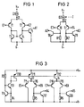
- the basic cell of a comparator consists, according to FIG. 1 of the drawing, for example of two emitter-coupled pnp transistors T1 and T2, at the bases of which input signals E1 and E2 are present as voltages occurring with respect to a reference potential, of a current mirror having two npn transistors T3 and T4, the base of which with the negative pole V- of the supply voltage source and the input or output of which is connected to the collector of one of the two transistors T1 and T2, from an npn transistor T5, the base of which is connected to the output of the current mirror and the emitter of which is connected to the negative pole V -
- the supply voltage source is connected and from a current injection Q1, which is connected between the positive pole V + of the supply voltage source and the coupled emitters of the transistors T1 and T2.
- the collector of the transistor T5 is here, like the bases of the transistors T1 and T2, optionally coupled to further switching elements.
- the one from the Current injection Q1 current I1 is essentially constant and depends on the temperature.
- a current mirror is usually used as such a load in comparator circuits.
- a common comparator circuit is known for example from LP 265 / LP 365 micropower programmable quad comparator, Linear Databook 1, National Semiconductor Corporation, Santa Clara, USA, pp. 4-67ff. If several comparators are now required in an integrated circuit, the current mirror with its two transistors represents a considerable amount of circuitry.
- the object of the invention is therefore to provide a comparator circuit with less effort.
- the comparator circuit according to the invention has two emitter-coupled pnp transistors T6 and T7.
- An input signal E3 is applied to the base of transistor T6 and an input signal E4 is applied to the base of transistor T7.
- the two input signals E3, E4 are voltages.
- the collectors of both transistors are each via a resistor R1 or R2 with the negative pole V- one not shown in the drawing Supply voltage source connected.
- the two resistors R1 and R2 are constructed identically, so that they have the same resistance value and the same temperature response.
- the resistors R1 and R2 are each connected in parallel with the base-emitter paths of two npn transistors T8 and T9.
- the switching state of the transistors T8 and T9 which represents the comparison result, can be picked off as signals A2 or A3 at the collector of the respective transistor.
- the coupled emitters of the transistors T6 and T7 are connected to the positive pole V + of the supply voltage source via a current injection Q2.
- the value of the current I2 impressed by the current impression Q2 and its dependence on the temperature T will be discussed in more detail elsewhere.
- the exemplary embodiment according to FIG. 3 shows an embodiment with several comparators, but only two are shown in the drawing. These each have two emitter-coupled pnp transistors T15, T16; T18, T19, at the bases of which input signals E5 to E8 are applied.
- In the collector line of a transistor T16; T19 are resistors R5; R6 switched, each of which the base-emitter path of an npn transistor T17; T20 is parallel.
- the emitters of the transistors T17; T20 are just like the collectors of the other transistors T15; T18 of the emitter-coupled transistors connected to the negative pole V- of the supply voltage source.
- the collectors of the transistors T16; T19 carry output signals A4 and A5.
- the coupled emitters of the transistors T15, T16; T18, T19 are each across the emitter-collector path of a pnp transistor T11; T12 connected to the positive pole V + of the supply voltage source.
- the coupled bases of the transistors T11; T12 are connected to the cathode of a diode leading to the positive pole V + of the supply voltage.
- the diode is formed by a pnp transistor T10, the base and the collector of which are connected to one another.
- the cathode of this diode is also across the collector-emitter path of an npn transistor T13 and a resistor R4 with the negative Pole V- of the supply voltage source coupled.
- Resistor R4 is connected in parallel with the base-emitter path of an npn transistor T14, the collector of which is connected to the base of transistor T13 and a resistor R3 leading to the positive pole V + of the supply voltage source.
- the diode-emitter formed by transistor T10 has the base-emitter paths of further pnp transistors connected in parallel, which form current impressions for further comparators, not shown in the drawing. All comparators, like the current impressions, are constructed identically. However, a different construction is possible to the same extent. However, this requires an adaptation, for example, via the transistors forming the current impressions.
- a very simple comparator uses only an ohmic resistance as a load instead of a current mirror between the emitter and the base of the output switching transistor - in the present exemplary embodiment, these are, for example, the transistors T8, T9, T17, T20.
- the load resistor - in the present exemplary embodiment these are the resistors R1, R2, R5, R6 - taking into account that in this case the collector currents of the two emitter-coupled transistors are each equal to half due to the current injection impressed current are dimensioned such that the respective load resistance is equal to the emitter-base threshold voltage of the respective output switching transistor divided by half the impressed current. Since the emitter-base threshold voltage of a transistor drops with increasing temperature, but resistors in integrated circuits have a positive temperature coefficient, ie have an increasing resistance with increasing temperature, the switching threshold of this simple comparator would be very temperature-dependent.
- the impressed current of the comparators is now - in the exemplary embodiment, these are the current I2 and the collector currents I3 and I4 of the transistors T11 and T12 - with the temperature so that the comparator switches independent of temperature if the input signal voltages are the same.
- the impressed current is now equal to the double quotient of the temperature-dependent emitter-base threshold voltage of the output switching transistor and the temperature-dependent load resistance and has the same temperature dependency.
- the value for the resistor R4 is equal to half the value of the load resistor, that is to say the value of the resistor R5 or R6.
- This half resistance value can easily be achieved, for example, by connecting two resistors which are constructed identically to the load resistor (ie resistor R5 or R6) in parallel.
- circuitry complexity in a comparator circuit according to the invention is considerably less than in known ones.
- the replacement of the current mirror, which still requires two transistor structures, with an easily implemented, low-cost resistor in the integrated circuit significantly reduces the space required in the integrated circuit, especially since the effort for temperature-dependent current injection does not increase compared to the previously used, temperature-independent current injection.
Landscapes
- Engineering & Computer Science (AREA)
- Physics & Mathematics (AREA)
- Microelectronics & Electronic Packaging (AREA)
- Nonlinear Science (AREA)
- Electromagnetism (AREA)
- General Physics & Mathematics (AREA)
- Radar, Positioning & Navigation (AREA)
- Automation & Control Theory (AREA)
- Measurement Of Current Or Voltage (AREA)
- Manipulation Of Pulses (AREA)
- Measuring Temperature Or Quantity Of Heat (AREA)
Claims (3)
- Circuit comparateur comportant des premier et second transistors (T6,T7; T15,T16; T18,T19) d'un premier type de conduction, aux bases desquels sont appliqués des signaux d'entrée (E3,E4; E5,E6; E7,E8) et dont les collecteurs sont reliés à un premier pôle (V-) d'une source de tension d'alimentation,
une première résistance (R2;R5,R6), qui est branchée dans la ligne du collecteur de l'un (T7,T16,T19) des deux transistors du premier type de conduction,
un premier transistor (T9,T17;T20) du second type de conduction et dont la section base-émetteur est branchée en parallèle avec la première résistance (R2;R5,R6) et au collecteur duquel est appliqué un signal de sortie (A3;A4,A5),
caractérisé par le fait
qu'il est prévu un circuit d'injection de courant (Q2; T10...T14, R3, R4), qui est branché entre les émetteurs couplés de premier et second transistors (T6,T7; T15,T16; T18,T19) du premier type de conduction et un second pôle (V+) de la source de tension d'alimentation, le courant (I2;I3,I4) injecté par le circuit d'injection de courant (Q2; T10...T14, R3, R4) étant, pour chaque température de fonctionnement, égal au double du quotient de la tension base-émetteur au point de commutation du premier transistor (T9;T17,T20) du second type de conduction, par la première résistance (R2;R5,R6), tandis qu'il est prévu, comme circuit d'injection de courant, un troisième transistor (T11,T12) du premier type de conduction, dont l'émetteur est relié au second pôle (V+) de la source de tension d'alimentation et dont le collecteur est relié aux émetteurs couplés de premier et second transistors (T6,T7; T15,T16; T18,T19) du premier type de conduction,
que la base du troisième transistor (T11,T12) du premier type de conduction est reliée d'une part dans le sens passant par l'intermédiaire d'une diode (T10) au second pôle (V+) de la source de tension d'alimentation et d'autre part par l'intermédiaire de la voie collecteur-émetteur d'un second transistor (T13) du second type de conduction et d'une seconde résistance (R4), au premier pôle (V-) de la source de tension d'alimentation,
que la base du second transistor (T13) du second type de conduction est reliée d'une part par l'intermédiaire d'une troisième résistance (R3) à l'autre pôle (V+) de la source de tension d'alimentation et d'autre part, par l'intermédiaire de la voie collecteur-émetteur d'un troisième transistor (T14) du second type de conduction, à un pôle (V-) de la source de tension d'alimentation, et
que la voie base-émetteur du troisième transistor (T14) du second type de conduction est branchée en parallèle avec la seconde résistance (R4). - Circuit comparateur suivant la revendication 1,
caractérisé par le fait
qu'une quatrième résistance (R1) ayant la même valeur résistive et le même comportement en température que la première résistance (R2) est branchée dans la ligne de collecteur de l'autre transistor (T6) du premier type de conduction, et
en parallèle avec la quatrième résistance (R1) est branchée la voie base-émetteur d'un quatrième transistor (T8) du second type de conduction, qui présente la même tension base-émetteur et le même comportement en température que le premier transistor (T9) du second type de conduction et sur le collecteur duquel est présent un autre signal de sortie (A2). - Circuit comparateur suivant l'une des revendications 1 ou 2, caractérisé par le fait que les voies base-émetteur d'autres transistors (T12) du premier type de conduction sont branchées en parallèle avec la voie base-émetteur du troisième transistor (T11) du premier type de conduction, les autres transistors (T12) étant prévus en tant que circuits d'injection de courant d'autres circuits comparateurs (T18,T19,T20,R6).
Priority Applications (4)
| Application Number | Priority Date | Filing Date | Title |
|---|---|---|---|
| EP90102815A EP0442001B1 (fr) | 1990-02-13 | 1990-02-13 | Circuit comparateur |
| ES90102815T ES2077594T3 (es) | 1990-02-13 | 1990-02-13 | Circuito comparador. |
| DE59009720T DE59009720D1 (de) | 1990-02-13 | 1990-02-13 | Komparatorschaltung. |
| US07/654,739 US5146114A (en) | 1990-02-13 | 1991-02-13 | Comparator circuit |
Applications Claiming Priority (1)
| Application Number | Priority Date | Filing Date | Title |
|---|---|---|---|
| EP90102815A EP0442001B1 (fr) | 1990-02-13 | 1990-02-13 | Circuit comparateur |
Publications (2)
| Publication Number | Publication Date |
|---|---|
| EP0442001A1 EP0442001A1 (fr) | 1991-08-21 |
| EP0442001B1 true EP0442001B1 (fr) | 1995-09-27 |
Family
ID=8203645
Family Applications (1)
| Application Number | Title | Priority Date | Filing Date |
|---|---|---|---|
| EP90102815A Expired - Lifetime EP0442001B1 (fr) | 1990-02-13 | 1990-02-13 | Circuit comparateur |
Country Status (4)
| Country | Link |
|---|---|
| US (1) | US5146114A (fr) |
| EP (1) | EP0442001B1 (fr) |
| DE (1) | DE59009720D1 (fr) |
| ES (1) | ES2077594T3 (fr) |
Cited By (1)
| Publication number | Priority date | Publication date | Assignee | Title |
|---|---|---|---|---|
| DE19708203A1 (de) * | 1997-02-28 | 1998-09-03 | Siemens Ag | Komparatorschaltung |
Families Citing this family (3)
| Publication number | Priority date | Publication date | Assignee | Title |
|---|---|---|---|---|
| US7084674B1 (en) | 2004-08-16 | 2006-08-01 | Analog Devices, Inc. | Differential amplifier with reduced common-mode and method |
| US20130292221A1 (en) * | 2012-05-01 | 2013-11-07 | James Ryan | Compact luggage |
| US11595033B2 (en) * | 2020-11-17 | 2023-02-28 | Texas Instruments Incorporated | Comparator architecture for reduced delay and lower static current |
Family Cites Families (12)
| Publication number | Priority date | Publication date | Assignee | Title |
|---|---|---|---|---|
| US3330972A (en) * | 1964-10-09 | 1967-07-11 | Gen Dynamics Corp | Sine wave threshold and phase comparator |
| US3588535A (en) * | 1967-08-22 | 1971-06-28 | Westinghouse Electric Corp | Control circuit with temperature compensation |
| JPS52114260A (en) * | 1976-03-22 | 1977-09-24 | Hitachi Ltd | Standard voltage generation circuit |
| JPS57557A (en) * | 1980-05-26 | 1982-01-05 | Toshiba Corp | Voltage comparator |
| JPS5711525A (en) * | 1980-06-25 | 1982-01-21 | Nec Corp | Comparing circuit |
| US4580069A (en) * | 1981-01-29 | 1986-04-01 | Motorola, Inc. | Comparator |
| JPS57173220A (en) * | 1981-04-17 | 1982-10-25 | Toshiba Corp | Comparator circuit |
| US4458201A (en) * | 1982-04-05 | 1984-07-03 | Burr-Brown Research Corp. | Digitally controlled precision current source with an open loop compensation circuit |
| JPS6054513A (ja) * | 1983-09-06 | 1985-03-29 | Nec Corp | 差動入力コンパレ−タ |
| US4542303A (en) * | 1983-10-03 | 1985-09-17 | Motorola, Inc. | Comparator circuit |
| JPS61116665A (ja) * | 1984-11-12 | 1986-06-04 | Fanuc Ltd | 低電力消費形電圧比較回路 |
| GB2197555B (en) * | 1986-10-02 | 1990-11-21 | Seikosha Kk | Comparator |
-
1990
- 1990-02-13 ES ES90102815T patent/ES2077594T3/es not_active Expired - Lifetime
- 1990-02-13 EP EP90102815A patent/EP0442001B1/fr not_active Expired - Lifetime
- 1990-02-13 DE DE59009720T patent/DE59009720D1/de not_active Expired - Lifetime
-
1991
- 1991-02-13 US US07/654,739 patent/US5146114A/en not_active Expired - Lifetime
Non-Patent Citations (2)
| Title |
|---|
| J.MARKUS: "Modern Electronic Circuit Reference Manual", McGraw-Hill, 1980, New York, US; Seite 3 * |
| P.HOROWITZ and W.HILL: "The Art of Electronics", Cambridge University Press, 1980, Cambridge, GB; Seiten 67-68 und 80-83 * |
Cited By (3)
| Publication number | Priority date | Publication date | Assignee | Title |
|---|---|---|---|---|
| DE19708203A1 (de) * | 1997-02-28 | 1998-09-03 | Siemens Ag | Komparatorschaltung |
| DE19708203C2 (de) * | 1997-02-28 | 1998-12-03 | Siemens Ag | Komparatorschaltung |
| US6064240A (en) * | 1997-02-28 | 2000-05-16 | Siemens Aktiengesellschaft | Comparator circuit with low current consumption |
Also Published As
| Publication number | Publication date |
|---|---|
| US5146114A (en) | 1992-09-08 |
| ES2077594T3 (es) | 1995-12-01 |
| EP0442001A1 (fr) | 1991-08-21 |
| DE59009720D1 (de) | 1995-11-02 |
Similar Documents
| Publication | Publication Date | Title |
|---|---|---|
| EP0288016B1 (fr) | Comparateur avec domaine étendu de signal d'entrée à mode commun | |
| DE68911708T2 (de) | Bandabstand-Referenzspannungsschaltung. | |
| EP0153492A1 (fr) | Circuit de protection pour appareils commandé par signaux électriques | |
| AT392375B (de) | Elektronische schaltung mit einem geschuetzten transistor | |
| DE2416534C3 (de) | Transistorschaltung zum Umkehren der Stromrichtung in einem Verbraucher | |
| EP0442001B1 (fr) | Circuit comparateur | |
| DE3486360T2 (de) | Differentialschalter. | |
| DE3012812C2 (fr) | ||
| DE3447002C2 (fr) | ||
| DE19624676C1 (de) | Schaltungsanordnung zur Erzeugung eines Referenzpotentials | |
| DE2804064A1 (de) | Verstaerkerschaltungsanordnung fuer aperiodische signale | |
| US4418321A (en) | Feedback amplifier or threshold value switch for a current feed differential stage | |
| EP0421016A1 (fr) | Convertisseur de niveau ECL-TTL | |
| DE3318957A1 (de) | Monolithisch integrierbare, bistabile multivibratorschaltung mit einem in einen vorzugszustand einstellbaren ausgang | |
| EP0246689B1 (fr) | Circuit pour convertir des signaux à trois états en signaux binaires | |
| EP0809169A2 (fr) | Circuit pour générer une tension de référence pouvant être validé ou inhibée | |
| DE2322466C3 (de) | Operationsverstärker | |
| DE3036736A1 (de) | Schaltungsanordnung zur belastungsproportionalen einstellung des ansteuerstroms eines in emitterschaltung betriebenen eintakt-endstufentransistors eines transistorverstaerkers | |
| USRE32479E (en) | Feedback amplifier or threshold value switch for a current feed differential stage | |
| DE1246027B (de) | Logische Schaltung aus zwei in Stromuebernahme-schaltung geschalteten Transistoren | |
| DE2612548C3 (de) | Integrierter Treiberbaustein mit bipolaren Transistoren, insbesondere zur Steuerung bipolarer Fernsprechrelais | |
| DE1638010C3 (de) | Festkörperschaltkreis für Referenzverstärker | |
| DE69031863T2 (de) | Elektronische Komparatorvorrichtung mit Hysterese | |
| DE3301800A1 (de) | Integrierbare schutzschaltung | |
| DE3418191C2 (fr) |
Legal Events
| Date | Code | Title | Description |
|---|---|---|---|
| PUAI | Public reference made under article 153(3) epc to a published international application that has entered the european phase |
Free format text: ORIGINAL CODE: 0009012 |
|
| 17P | Request for examination filed |
Effective date: 19901205 |
|
| AK | Designated contracting states |
Kind code of ref document: A1 Designated state(s): AT BE CH DE DK ES FR GB GR IT LI LU NL SE |
|
| RBV | Designated contracting states (corrected) |
Designated state(s): BE DE ES FR GB IT NL SE |
|
| 17Q | First examination report despatched |
Effective date: 19931117 |
|
| GRAA | (expected) grant |
Free format text: ORIGINAL CODE: 0009210 |
|
| AK | Designated contracting states |
Kind code of ref document: B1 Designated state(s): BE DE ES FR GB IT NL SE |
|
| REF | Corresponds to: |
Ref document number: 59009720 Country of ref document: DE Date of ref document: 19951102 |
|
| REG | Reference to a national code |
Ref country code: ES Ref legal event code: FG2A Ref document number: 2077594 Country of ref document: ES Kind code of ref document: T3 |
|
| ITF | It: translation for a ep patent filed | ||
| GBT | Gb: translation of ep patent filed (gb section 77(6)(a)/1977) |
Effective date: 19951212 |
|
| ET | Fr: translation filed | ||
| PLBE | No opposition filed within time limit |
Free format text: ORIGINAL CODE: 0009261 |
|
| STAA | Information on the status of an ep patent application or granted ep patent |
Free format text: STATUS: NO OPPOSITION FILED WITHIN TIME LIMIT |
|
| 26N | No opposition filed | ||
| PGFP | Annual fee paid to national office [announced via postgrant information from national office to epo] |
Ref country code: ES Payment date: 19970213 Year of fee payment: 8 Ref country code: SE Payment date: 19970213 Year of fee payment: 8 |
|
| PGFP | Annual fee paid to national office [announced via postgrant information from national office to epo] |
Ref country code: BE Payment date: 19970221 Year of fee payment: 8 |
|
| PGFP | Annual fee paid to national office [announced via postgrant information from national office to epo] |
Ref country code: NL Payment date: 19970225 Year of fee payment: 8 |
|
| PG25 | Lapsed in a contracting state [announced via postgrant information from national office to epo] |
Ref country code: SE Free format text: LAPSE BECAUSE OF NON-PAYMENT OF DUE FEES Effective date: 19980214 Ref country code: ES Free format text: LAPSE BECAUSE OF NON-PAYMENT OF DUE FEES Effective date: 19980214 |
|
| PG25 | Lapsed in a contracting state [announced via postgrant information from national office to epo] |
Ref country code: BE Free format text: LAPSE BECAUSE OF NON-PAYMENT OF DUE FEES Effective date: 19980228 |
|
| BERE | Be: lapsed |
Owner name: SIEMENS A.G. Effective date: 19980228 |
|
| PG25 | Lapsed in a contracting state [announced via postgrant information from national office to epo] |
Ref country code: NL Free format text: LAPSE BECAUSE OF NON-PAYMENT OF DUE FEES Effective date: 19980901 |
|
| EUG | Se: european patent has lapsed |
Ref document number: 90102815.9 |
|
| NLV4 | Nl: lapsed or anulled due to non-payment of the annual fee |
Effective date: 19980901 |
|
| REG | Reference to a national code |
Ref country code: ES Ref legal event code: FD2A Effective date: 20000403 |
|
| PGFP | Annual fee paid to national office [announced via postgrant information from national office to epo] |
Ref country code: GB Payment date: 20010208 Year of fee payment: 12 |
|
| REG | Reference to a national code |
Ref country code: GB Ref legal event code: IF02 |
|
| PG25 | Lapsed in a contracting state [announced via postgrant information from national office to epo] |
Ref country code: GB Free format text: LAPSE BECAUSE OF NON-PAYMENT OF DUE FEES Effective date: 20020213 |
|
| GBPC | Gb: european patent ceased through non-payment of renewal fee |
Effective date: 20020213 |
|
| PGFP | Annual fee paid to national office [announced via postgrant information from national office to epo] |
Ref country code: IT Payment date: 20090221 Year of fee payment: 20 Ref country code: DE Payment date: 20090416 Year of fee payment: 20 |
|
| PGFP | Annual fee paid to national office [announced via postgrant information from national office to epo] |
Ref country code: FR Payment date: 20090213 Year of fee payment: 20 |
|
| PG25 | Lapsed in a contracting state [announced via postgrant information from national office to epo] |
Ref country code: DE Free format text: LAPSE BECAUSE OF EXPIRATION OF PROTECTION Effective date: 20100213 |