EP0441958B1 - Phosphor-röntgenbildschirm und verfahren zu dessen herstellung - Google Patents
Phosphor-röntgenbildschirm und verfahren zu dessen herstellung Download PDFInfo
- Publication number
- EP0441958B1 EP0441958B1 EP90914577A EP90914577A EP0441958B1 EP 0441958 B1 EP0441958 B1 EP 0441958B1 EP 90914577 A EP90914577 A EP 90914577A EP 90914577 A EP90914577 A EP 90914577A EP 0441958 B1 EP0441958 B1 EP 0441958B1
- Authority
- EP
- European Patent Office
- Prior art keywords
- cube
- ray
- retro
- array
- wafer
- Prior art date
- Legal status (The legal status is an assumption and is not a legal conclusion. Google has not performed a legal analysis and makes no representation as to the accuracy of the status listed.)
- Expired - Lifetime
Links
Images

Classifications
-
- C—CHEMISTRY; METALLURGY
- C30—CRYSTAL GROWTH
- C30B—SINGLE-CRYSTAL GROWTH; UNIDIRECTIONAL SOLIDIFICATION OF EUTECTIC MATERIAL OR UNIDIRECTIONAL DEMIXING OF EUTECTOID MATERIAL; REFINING BY ZONE-MELTING OF MATERIAL; PRODUCTION OF A HOMOGENEOUS POLYCRYSTALLINE MATERIAL WITH DEFINED STRUCTURE; SINGLE CRYSTALS OR HOMOGENEOUS POLYCRYSTALLINE MATERIAL WITH DEFINED STRUCTURE; AFTER-TREATMENT OF SINGLE CRYSTALS OR A HOMOGENEOUS POLYCRYSTALLINE MATERIAL WITH DEFINED STRUCTURE; APPARATUS THEREFOR
- C30B29/00—Single crystals or homogeneous polycrystalline material with defined structure characterised by the material or by their shape
- C30B29/02—Elements
- C30B29/06—Silicon
-
- C—CHEMISTRY; METALLURGY
- C30—CRYSTAL GROWTH
- C30B—SINGLE-CRYSTAL GROWTH; UNIDIRECTIONAL SOLIDIFICATION OF EUTECTIC MATERIAL OR UNIDIRECTIONAL DEMIXING OF EUTECTOID MATERIAL; REFINING BY ZONE-MELTING OF MATERIAL; PRODUCTION OF A HOMOGENEOUS POLYCRYSTALLINE MATERIAL WITH DEFINED STRUCTURE; SINGLE CRYSTALS OR HOMOGENEOUS POLYCRYSTALLINE MATERIAL WITH DEFINED STRUCTURE; AFTER-TREATMENT OF SINGLE CRYSTALS OR A HOMOGENEOUS POLYCRYSTALLINE MATERIAL WITH DEFINED STRUCTURE; APPARATUS THEREFOR
- C30B33/00—After-treatment of single crystals or homogeneous polycrystalline material with defined structure
-
- G—PHYSICS
- G21—NUCLEAR PHYSICS; NUCLEAR ENGINEERING
- G21K—HANDLING OF PARTICLES OR IONISING RADIATION NOT OTHERWISE PROVIDED FOR; IRRADIATION DEVICES; GAMMA RAY OR X-RAY MICROSCOPES
- G21K4/00—Conversion screens for the conversion of the spatial distribution of X-rays or particle radiation into visible images, e.g. fluoroscopic screens
Definitions
- This invention relates to x-ray imaging screens of the type employing x-ray stimulable phosphors to generate light emissions which are then used to expose photosensitive films or light sensitive solid state sensors to generate the x-ray image.
- x-ray imaging screen in which a layer of phosphor is used to intercept x-rays in, for example, the 15-115 keV energy range to generate photoemissions which are then used to expose a photosensitive film or a light sensitive solid state sensor to generate the desired x-ray image.
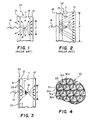
- Fig. 1 An example of such a screen is shown in Fig. 1, wherein the x-ray imaging screen 10 comprises a phosphor layer 11 formed on a substrate 12 and a photosensitive film sheet 13 pressed against the phosphor side of the screen.
- the particle fluoresces thus emitting light rays relatively uniformly in all directions as indicated by the arrows in Fig. 1.
- Those light rays which exit the phospher layer through the right-hand surface 16 enter the light sensitive film 13 and expose the film emulsion.
- the film can then be processed using conventional developing techniques to bring out a permanent record of the x-ray image formed on the film.
- An advantage of this arrangement over the use of direct exposure of the film to the x-ray energy lies in the greater sensitivity of the screen achieved by suitable selection of the phosphor material with high atomic numbers to increase the x-ray absorption efficiency of the screen.
- Light collection efficiency of an arrangement of this type can be increased by sandwiching the phosphor layer between two sheets of film thus capturing the light rays that escape from both facial surfaces of the phosphor screen.
- the composite image is then created by superimposing the two films after development.
- Another known approach to increasing sensitivity is shown in the modified screen 10' of Fig. 2 wherein mirror 18 is positioned on the left-hand side of the screen opposite the film 13. The light rays which would normally exit from this non-film side of the phosphor layer 11 are reflected by the mirror 18 to the film. Rather than using a seperate mirror, the same effect may also be created by aluminizing the surface 12a of the phosphor substrate 12 prior to depositing the phosphor.
- Fig. 2 Although the mirrored arrangement of Fig. 2 has the advantage of improving the light collection efficiency and therefore the sensitivity of the screen, it has the disadvantage that resolution is degraded by virtue of the increased effective spot size d' resulting from the reflected light, as compared to the smaller spot size d in Fig. 1 which results solely from the direct light rays.
- U.S. Patent No. 4,912,333 discloses only the use of lenslets in the form of microbeads as the retro-reflective medium. Effective as they are for this purpose, they have certain deficiencies resulting from the fact that close packed beads inherently have voids therebetween that reduce the reflection efficiency. They also have bands around the outer circumference of each bead that do not act as reflectors.
- an x-ray imaging phosphor screen and a method of making a planar array corner cube surface which comprises the steps of forming a wafer of single crystal material, such as silicon, having a cubic lattice structure with the facial surface of the wafer oriented in a ⁇ 111 ⁇ plane of the cubic structure, forming on the facial surface of the wafer a photoresist pattern of an array of equilateral triangle openings, the sides of the triangle openings being parallel to the ⁇ 110> directions of the cubic lattice in said ⁇ 111 ⁇ plane of the facial surface of the cubic structure, the parallel sides of adjacent triangle openings being spaced apart by a predetermined amount throughout the array pattern and etching said crystal material with an anisotropic etchant adapted to preferentially etch ⁇ 100 ⁇ planes of the cubic lattice structure to form a corresponding array of internal corner cu
- a retro-reflective sheet suitable for use as a back reflector for an x-ray stimulable phosphor imaging screen may be produced by forming a negative master of the corner cube surface, as by metal plating, and separating the negative master from the single crystal surface. A sheet having a planar array corner cube surface matching that of the etched crystal is then formed on the negative master, as by any molding process. After removal of the sheet from the negative master, the corner cube surface is made reflective by any suitable means such as evaporation of aluminum onto the surface.
- Figs. 1 and 2 effectively illustrate the dilemma between light collection efficiency and image resolution when a planar mirror surface is used to increase efficiency of the phosphor screen by reflecting light rays that would otherwise be lost to the photosensitive film.
- the mirror 18 in Fig. 2 reflects the fluorescent light rays outward thus significantly increasing the area of the spot size d' on the film 13 as compared to spot size d in the screen of Fig. 1.
- FIG. 3 A presently preferred embodiment of the imaging screen of the invention is illustrated in Fig. 3, wherein the planar mirror 18 of Fig. 2 is replaced by a sheet 20 having a corner cube retro-reflective surface 21 positioned facing the facial surface 22 of the phosphor layer 11.
- sheet 20 is positioned in contact with the outer surface of substrate 12 on which the phosphor layer 11 is deposited.
- the phosphor layer 11 may be deposited directly on sheet 20 thus eliminating the intermediate substrate 12.
- the drawings are not to scale, but are drawn so as to best illustrate the concepts involved.
- the materials used for fabrication of the retro-reflective sheet preferably should be substantially transparent to the x-radiation to be detected so as to allow penetration of the x-rays into the phosphor layer 11.
- Retro-reflective surfaces are known to exhibit the characteristic of reflecting incident light back substantially along an axis parallel to the axis of the incident light illumination as shown by double arrow 17.
- a corner cube retro-reflector surface As is known, a corner cube retro-reflector surface, best seen in Fig. 4, consists of a planar array of three-sided, interior pyramidal surfaces such as would be formed by the intersection of the corner of a cube by a plane normal to a line joining diametrically opposed corners of the cube.
- each interior pyramidal surface is formed by base lines 31a-31c lying in the plane of the paper and defining an open equilateral triangular aperture and by three planar sides 32a-32c defining isosceles triangle surfaces meeting at a common apex 23 positioned below the plane of the paper.
- These interior pyramidal surfaces are coated with a suitable reflective surface treatment, e.g. by aluminizing, to form the desired retro-reflective surface 21 (Fig. 3).
- the aperture of the reflector cell ideally should be very small in comparison to the distance of the light source from the aperture in order to preserve the desired resolution in the image created on film 13.
- the distance from the light source to the retro-reflective surface is dependent on the distance the x-ray penetrates into the phosphor layer before it is absorbed thereby creating a fluorescent event (plus the thickness of the phosphor substrate, if one is employed between the phosphor layer and the reflector surface).
- a thicker phosphor layer would increase the absorption efficiency of the screen and simultaneously increase the mean distance of phosphor events from the retroreflector surface, the maximum thickness is constrained by light scatter considerations which can degrade image resolution. Fluorescent events occurring remote from the film layer, corresponding to minimal x-ray penetration of the phosphor layer, inherently create a larger diameter spot on the film than events occurring close to the film layer. For typical x-ray phosphor compositions, a thickness range of from 50 microns to 200 microns is generally considered acceptable.
- the aperture of the reflector cell is about 50 microns, or smaller, as measured along an orthogonal line extending from one of the baselines 31a-31c to the corresponding opposite apex lying in the plane of the paper.
- the minimum aperture size is limited by the wavelength of the incident fluorescent light rays in order to avoid the effects of diffraction. For this reason, the minimum aperture size is about 10 ⁇ , where ⁇ is the wavelength of the incident light ray.
- a reflector cell aperture of about 5 microns would thus give preferred retro-reflection characteristics for screens of the type being considered, although larger aperture sizes up to about 50 microns should also work satisfactorily, as previously noted.
- a suitable corner cube reflector surface with apertures of this small size may be produced from single crystal cubic lattice silicon wafers which have been etched with an anisotropic etchant to produce a master pattern of corner cube reflector cells.
- an anisotropic etchant to produce a master pattern of corner cube reflector cells.
- the cube "abcdefgh” has six face planes, each of which can be specified by a set of three coordinates representing normalized intercepts of three mutually orthogonal reference axes.
- face “abcd” is represented in Miller indices within parentheses as the (100) plane and face “efgh” is represented as the ( 1 ⁇ 00) plane.
- All planes of equivalent symmetry can be represented by a single expression using curly brackets (braces) in place of the parentheses.
- curly brackets braces
- all cube face planes are represented by the expression ⁇ 100 ⁇ while all of the above-described canted planes of the cube can be represented by the expression ⁇ 111 ⁇ .
- Directions in a cube crystal are expressed in integers of a vector in the desired direction referred to the axis vectors and are written in square brackets [ ] to represent individual directions or in angled brackets ⁇ > to denote all directions of equivalent symmetry.
- the "x" axis "ea” is the [100] direction and the "-x” axis “ae” is the [ 1 ⁇ 00] direction.
- the line “af” in Fig. 5 is in the [ 1 ⁇ 01] direction while “fa” is in the [10 1 ⁇ ] direction.
- a full set of equivalent directions is thus expressed as ⁇ 110> with the subsets [ 1 ⁇ 01], [10 1 ⁇ ], [01 1 ⁇ ], [0 1 ⁇ 1], [1 1 ⁇ 0] and [ 11 ⁇ 0] being the directions of the three lines of intersection of the illustrated (111) plane in the cube faces. It will be appreciated that each of the equivalent symmetry planes ⁇ 111 ⁇ will have a corresponding subset of associated directions included within the expression ⁇ 111>.
- a wafer of single crystal material having cubic crystal symmetry preferably silicon
- a layer of photoresist material is then coated onto the facial surface of the wafer.
- a pattern of an array of close packed equilateral triangle openings is formed in the photoresist layer.
- the triangle openings are oriented in the pattern with the sides of each triangle parallel to the ⁇ 110> directions of the cube lattice structure lying in the ⁇ 111 ⁇ plane of the facial surface of the wafer and with parallel sides of adjacent triangle openings spaced apart by a predetermined amount as will be explained later.
- This physical arrangement may best be visualized with reference to the diagram of Fig. 6 which illustrates the geometric orientation of triangle openings 40 relative to the cubic lattice structure shown in Fig. 5.
- a layer of photoresist material 42 has formed therein a pattern of a close packed array of equilateral triangle openings 40.
- the sides of the triangle openings are oriented parallel to the ⁇ 110> directions of the cube lattice structure (lines ag, gf, and fa in Fig. 5) lying in the ⁇ 111 ⁇ plane of the facial surface of the single cube silicon wafer 44 (Fig. 7) on which the layer of photoresist material is deposited.
- a silicon wafer is produced with a reference edge cut in one side of the wafer to indicate the cube lattice orientation of the wafer.
- This reference edge can be specified to be cut parallel to a ⁇ 110> direction to indicate the desired physical orientation of the wafer relative to the crystal axes.
- a corresponding reference edge is incorporated in the mask parallel to a triangle side which may then be aligned with the reference edge of the wafer to assure proper alignment of the mask on the photoresist layer to achieve parallelism between the triangle openings and the ⁇ 110> directions of the cube lattice structure.
- FIG. 7 illustrates schematically the stages of development of the corner cube pattern beginning with the deposition of photoresist layer 42 on the silicon wafer 44.
- a plurality of properly oriented triangle openings 40 are formed in the photoresist layer 42.
- An anisotropic etchant selected to preferentially etch ⁇ 100 ⁇ planes of the cubic lattice structure of the silicon wafer 44 is then flowed in a known manner over the surface to the photoresist pattern to begin anisotropic etching of the ⁇ 100 ⁇ planes 32a-32c.
- etchants to achieve anisotropic etching of ⁇ 100 ⁇ planes in silicon are described in the book Integrated Circuit Fabrication Technology by David J. Elliott and published by McGraw-Hill Book Company, 1982, on pages 248-250.
- etching commences along the ⁇ 100 ⁇ planes 32a-32c, as represented by arrows 45 in Fig 7c, the process continues along the selected ⁇ 100 ⁇ planes with an increasing cavity size as the ⁇ 111 ⁇ plane surface 46 gradually decreases in each created cell.
- the process is completed when the ⁇ 111 ⁇ plane is fully depleted and the ⁇ 100 ⁇ planes 31a-31c meet at apex 23.
- the spacing between adjacent parallel sides of the triangle openings in the photoresist pattern is determined relative to the etch rate of the chosen etchant to allow the ⁇ 100 ⁇ planes of adjacent corner cubes to meet at the baselines of intersection 31a-31c corresponding to the ⁇ 110> directions in the facial surface of wafer 44 at least by the time the anisotropic etching of the corner cube is completed.
- the photoresist material 42 is washed off the silicon in known manner to thus leave the desired corner cube surface.
- the resulting corner cube surface on the face of wafer 44 may then serve as a pattern to form a negative master by plating a metal on the wafer which may then be separated from the wafer by peeling apart or dissolving the silicon.
- This metal master can then be coated with a suitable material such as is used in making film substrates to create the corner cube sheet 20 of Fig. 4 which, after hardening and removal, can be reflectorized, for example by evaporation of aluminum on the corner cube surface of the sheet.
- silicon wafers are produced in relatively small dimensions, typically in circular wafers of about six inches in diameter.
- a plurality of silicon wafers cut to suitable square or rectangular dimensions can be etched to prepare the master corner cube surface after which the wafers may be abutted to create the desired size of sheet. Cutting of the wafers may be done before or after the etching process.
Landscapes
- Chemical & Material Sciences (AREA)
- Engineering & Computer Science (AREA)
- Materials Engineering (AREA)
- Organic Chemistry (AREA)
- Metallurgy (AREA)
- Crystallography & Structural Chemistry (AREA)
- High Energy & Nuclear Physics (AREA)
- Physics & Mathematics (AREA)
- General Engineering & Computer Science (AREA)
- Conversion Of X-Rays Into Visible Images (AREA)
- Optical Elements Other Than Lenses (AREA)
- Measurement Of Radiation (AREA)
- Weting (AREA)
Claims (10)
- Röntgenbildschirm, der Röntgenstrahlen stimulierenden Phosphor enthält, um Lichtemissionen zu erzeugen, die für die Belichtung lichtempfindlicher Filme (13) oder lichtempfindlicher Halbleitersensoren verwendet werden, um ein Röntgenbild zu erzeugen; wobei der Leuchtschirm eine Phosphorschicht (11) und reflektierende Mittel (18; 20) aufweist, die in Kontakt mit einer Außenfläche einer Unterlage (12) angeordnet sind, auf der die Phosphorschicht (11) aufgebracht ist und die der Frontfläche (12a, 22) der Phosphorschicht gegenüber der Seite der Phosphorschicht, an die der Film zur Belichtung angedrückt wird, gegenüberliegt; dadurch gekennzeichnet, daß die reflektierenden Mittel (20) aus einer Platte bestehen, die eine Corner-Cube-Fläche aufweist, welche mit einem lichtreflektierenden oberflächenbelag beschichtet ist und dadurch eine retroreflektierende Fläche (21) bildet, die so angeordnet ist, daß sie der Frontfläche (22) der Phosphorschicht (11) gegenüberliegt und einen Retroreflektor mit in der Phosphorschicht entstehenden Lichtquellen (15) bildet.
- Röntgenbildschirm nach Anspruch 1, dadurch gekennzeichnet, daß die Corner-Cubes der retroreflektierenden Fläche (21) eine öffnungsgröße zwischen maximal 50 Mikrometer (1,27 mm) und mindestens etwa der zehnfachen Wellenlänge des einfallenden Lichtstrahls für eine Phosphorschicht mit einem Dickenbereich von 1,27 mm (50 Mikrometer) bis 5,08 mm (200 Mikrometer) besitzen, so daß die Röntgenstrahleneinfalls- und -reflektionsachse zusammenfallen.
- Röntgenbildschirm nach Anspruch 1 oder 2, dadurch gekennzeichnet, daß die Corner-Cube retroreflektierende Fläche (21) aus einer planaren Anordnung dreiseitiger, nach innen gerichteter Pyramidenflächen besteht, die durch den Schnitt einer Würfelecke durch eine Ebene gebildet werden, die sich senkrecht zu einer Linie erstreckt, welche diagonal gegenüberliegende Würfelecken verbindet.
- Röntgenbildschirm nach Anspruch 3, dadurch gekennzeichnet, daß jede nach innen gerichtete Pyramidenfläche durch Grundlinien (31a, 31b, 31c) gebildet wird, die in dieser Ebene liegen und die Öffnung als offene, gleich-seitige, dreieckige Öffnung definieren, und durch drei ebene Seiten (32a, 32b, 32c), welche gleichschenklige Dreiecksflächen bilden, die sich in einem gemeinsamen Schnittpunkt (23) treffen, der sich unter der Ebene der Platte (20) befindet, die der Frontfläche (22) gegenüberliegt.
- Röntgenbildschirm nach Anspruch 1, 2 oder 4, dadurch gekennzeichnet, daß die Platte (20) bzw. ihre retroreflektierende Fläche (21) für zu erfassende Röntgenstrahlung im wesentlichen durchlässig ist, so daß die Röntgenstrahlen in die Phosphorschicht (11) eindringen können.
- Verfahren zum Herstellen eines Phosphor-Röntgenbildschirms mit folgenden Schritten:- Erzeugen eines Substrats (44) aus Einkristallmaterial mit einer kubischen Gitterstruktur, wobei die Hauptfläche des Substrats in einer Ebene (100) der kubischen Struktur ausgerichtet ist;- Erzeugen eines Fotolackmusters (42) einer geordneten Reihe eng beabstandeter, gleichseitiger öffnungen (40) auf der Hauptfläche des Substrats, wobei benachbarte Öffnungen gepaarte, gleichverlaufende, parallele Seiten aufweisen, und wobei die Seiten der Dreiecksöffnungen zu den Richtungen <110> des kubischen Gitters in der Ebene {111} der Hauptfläche der kubischen Struktur parallel verlaufen, und die parallelen Seiten benachbarter Öffnungen über das gesamte Muster durch einen vorbestimmten Betrag voneinander beabstandet sind;- Ätzen des Kristallmaterials mit Hilfe eines anisotropen Ätzmittels, das vornehmlich Ebenen {100} der kubischen Gitterstruktur ätzt und eine entsprechende Reihe nach innen gerichteter Pyramidenflächen unter den öffnungen des Fotolackmusters erzeugt; und- Entfernen des Fotolackmusters, wonach auf der Substrathauptfläche eine planparallele Kubenanordnung verbleibt;
gekennzeichnet durch folgende Schritte:- Bilden einer Negativstruktur aus der planparallelen Kubenanordnung;- Herstellen einer Platte (20) mit ausreichender Dicke eines für Röntgenstrahlen im wesentlichen durchlässigen Materials auf der Negativstruktur mit einem kompletten positiven Duplikat der planparallelen Kubenanordnung, die auf einer Seite der Platte ausgebildet ist;- Trennen der Platte von der Negativstruktur;- Beschichten der Corner-Cube-Fläche der Platte mit einem für Röntgenstrahlen im wesentlichen durchlässigen, lichtreflektierenden Material, um eine retroreflektierende Corner-Cube-Fläche (21) zu erzeugen;- Erzeugen einer Schicht (11) aus Röntgenstrahlen absorbierendem, lichtemittierendem Phosphor; und- Anlegen der Platte an die Phosphorschicht, wobei die retroreflektierende Corner-Cube-Fläche gegenüber der Phosphorschicht zu liegen kommt. - Verfahren nach Anspruch 6, dadurch gekennzeichnet, daß das Fotolackmuster als eine Reihe eng beabstandeter Öffnungen (40) aus gleichseitigen Dreiecken gebildet wird; und daß unter den Dreiecksöffnungen des Fotolackmusters eine Anordnung nach innen gerichteter Corner-Cube Pyramidenflächen gebildet wird, so daß zwischen benachbarten Corner-Cubes im wesentlichen keine restliche Planfläche verbleibt.
- Verfahren nach Anspruch 7, dadurch gekennzeichnet, daß die gepaarten, gleichverlaufenden, parallelen Seiten benachbarter Dreiecksöffnungen über das gesamte Muster hinweg einen gleichen Abstand voneinander haben.
- Verfahren nach Anspruch 6, dadurch gekennzeichnet, daß die Platte (44) aus Einkristall-Silizium besteht.
- Verfahren nach Anspruch 8 oder 9, dadurch gekennzeichnet, daß der Abstand zwischen den gepaarten, gleichverlaufenden, parallelen Seiten benachbarter Dreiecksöffnungen so groß ist, daß sich Ebenen {100} benachbarter Corner-Cubes zumindest dann treffen, wenn das anisotrope Ätzen der Corner-Cubes abgeschlossen ist.
Applications Claiming Priority (3)
| Application Number | Priority Date | Filing Date | Title |
|---|---|---|---|
| US07/403,246 US4992699A (en) | 1989-09-05 | 1989-09-05 | X-ray phosphor imaging screen and method of making same |
| US403246 | 1989-09-05 | ||
| PCT/US1990/004911 WO1991003816A1 (en) | 1989-09-05 | 1990-08-29 | X-ray phosphor imaging screen and method of making same |
Publications (2)
| Publication Number | Publication Date |
|---|---|
| EP0441958A1 EP0441958A1 (de) | 1991-08-21 |
| EP0441958B1 true EP0441958B1 (de) | 1996-04-03 |
Family
ID=23595068
Family Applications (1)
| Application Number | Title | Priority Date | Filing Date |
|---|---|---|---|
| EP90914577A Expired - Lifetime EP0441958B1 (de) | 1989-09-05 | 1990-08-29 | Phosphor-röntgenbildschirm und verfahren zu dessen herstellung |
Country Status (5)
| Country | Link |
|---|---|
| US (1) | US4992699A (de) |
| EP (1) | EP0441958B1 (de) |
| JP (1) | JP2892829B2 (de) |
| DE (1) | DE69026369T2 (de) |
| WO (1) | WO1991003816A1 (de) |
Families Citing this family (20)
| Publication number | Priority date | Publication date | Assignee | Title |
|---|---|---|---|---|
| US5391259A (en) * | 1992-05-15 | 1995-02-21 | Micron Technology, Inc. | Method for forming a substantially uniform array of sharp tips |
| US5753130A (en) | 1992-05-15 | 1998-05-19 | Micron Technology, Inc. | Method for forming a substantially uniform array of sharp tips |
| US5416821A (en) * | 1993-05-10 | 1995-05-16 | Trw Inc. | Grid formed with a silicon substrate |
| CA2131243A1 (en) * | 1993-09-27 | 1995-03-28 | Kenneth R. Paulson | Process for forming a phosphor |
| US5695658A (en) * | 1996-03-07 | 1997-12-09 | Micron Display Technology, Inc. | Non-photolithographic etch mask for submicron features |
| US6461003B1 (en) | 1997-06-12 | 2002-10-08 | Purdue Research Foundation | Corner cube arrays and manufacture thereof |
| WO1998056966A1 (en) * | 1997-06-12 | 1998-12-17 | Purdue Research Foundation | Corner cube arrays and manufacture thereof |
| US6177236B1 (en) * | 1997-12-05 | 2001-01-23 | Xerox Corporation | Method of making a pixelized scintillation layer and structures incorporating same |
| US5981959A (en) * | 1997-12-05 | 1999-11-09 | Xerox Corporation | Pixelized scintillation layer and structures incorporating same |
| US6174449B1 (en) | 1998-05-14 | 2001-01-16 | Micron Technology, Inc. | Magnetically patterned etch mask |
| JP4053260B2 (ja) * | 2000-10-18 | 2008-02-27 | シャープ株式会社 | 有機エレクトロルミネッセンス表示素子 |
| KR100490816B1 (ko) * | 2001-06-15 | 2005-05-24 | 샤프 가부시키가이샤 | 마이크로 코너 큐브 어레이, 마이크로 큐브 어레이의 제조방법 및 반사형 표시 장치 |
| JP3818906B2 (ja) * | 2001-12-13 | 2006-09-06 | シャープ株式会社 | マイクロコーナーキューブアレイ、その作製方法、および表示装置 |
| JP2004086164A (ja) * | 2002-06-27 | 2004-03-18 | Sharp Corp | コーナーキューブアレイおよびその作製方法 |
| US7201485B1 (en) | 2003-08-15 | 2007-04-10 | University Of South Florida | Corner cube retroreflector |
| JP4772102B2 (ja) * | 2008-10-31 | 2011-09-14 | シャープ株式会社 | コーナーキューブアレイの作製方法 |
| US9261301B2 (en) | 2013-05-28 | 2016-02-16 | M & M Electric Service, Inc. | Vehicle-transportable ice plant |
| CN105329847A (zh) * | 2014-08-15 | 2016-02-17 | 中国科学院物理研究所 | 一种微腔结构阵列的制备方法 |
| JP6457099B2 (ja) * | 2015-09-08 | 2019-01-23 | シャープ株式会社 | 波長変換部材および発光装置 |
| US11753991B2 (en) | 2019-06-25 | 2023-09-12 | Yantai Jereh Petroleum Equipment & Technologies Co., Ltd. | Intake-exhaust transport apparatus mobile power generation system and assembling method thereof |
Family Cites Families (9)
| Publication number | Priority date | Publication date | Assignee | Title |
|---|---|---|---|---|
| US2882413A (en) * | 1953-12-04 | 1959-04-14 | Vingerhoets Antonius Wilhelmus | Luminescent screen |
| US3944835A (en) * | 1974-09-25 | 1976-03-16 | General Electric Company | High energy radiation detector having improved reflective backing for phosphor layer |
| US4025662A (en) * | 1974-12-05 | 1977-05-24 | The United States Of America As Represented By The Secretary Of The Army | Method for making ultra high resolution phosphor screens |
| JPS53120376A (en) * | 1977-03-30 | 1978-10-20 | Fujitsu Ltd | Production of semiconductor device |
| NL7806828A (nl) * | 1978-06-26 | 1979-12-28 | Philips Nv | Luminescentiescherm. |
| US4227942A (en) * | 1979-04-23 | 1980-10-14 | General Electric Company | Photovoltaic semiconductor devices and methods of making same |
| JPS5949141A (ja) * | 1982-09-13 | 1984-03-21 | Shimadzu Corp | X線螢光増倍管の入力面 |
| JPS5993000A (ja) * | 1982-11-17 | 1984-05-29 | Yoshihiro Hamakawa | 単結晶薄膜製造用基板 |
| JPS59202100A (ja) * | 1983-04-30 | 1984-11-15 | コニカ株式会社 | 放射線画像変換パネル及びその製造方法 |
-
1989
- 1989-09-05 US US07/403,246 patent/US4992699A/en not_active Expired - Fee Related
-
1990
- 1990-08-29 DE DE69026369T patent/DE69026369T2/de not_active Expired - Fee Related
- 1990-08-29 WO PCT/US1990/004911 patent/WO1991003816A1/en not_active Ceased
- 1990-08-29 JP JP2513712A patent/JP2892829B2/ja not_active Expired - Lifetime
- 1990-08-29 EP EP90914577A patent/EP0441958B1/de not_active Expired - Lifetime
Also Published As
| Publication number | Publication date |
|---|---|
| DE69026369T2 (de) | 1996-10-31 |
| JP2892829B2 (ja) | 1999-05-17 |
| WO1991003816A1 (en) | 1991-03-21 |
| JPH04501614A (ja) | 1992-03-19 |
| US4992699A (en) | 1991-02-12 |
| DE69026369D1 (de) | 1996-05-09 |
| EP0441958A1 (de) | 1991-08-21 |
Similar Documents
| Publication | Publication Date | Title |
|---|---|---|
| EP0441958B1 (de) | Phosphor-röntgenbildschirm und verfahren zu dessen herstellung | |
| EP0126564B1 (de) | Verfahren zur Wiedergabe eines Strahlungsbildes | |
| US5418377A (en) | Pixelized phosphor | |
| EP0233497B1 (de) | Strahlungsbildspeicherplatte | |
| US5302423A (en) | Method for fabricating pixelized phosphors | |
| JPS60103310A (ja) | マイクロフレネルレンズの製造方法 | |
| JPH0682604B2 (ja) | X線マスク | |
| KR970010364B1 (ko) | 인광 물질의 제조 방법 | |
| GB2231684A (en) | Method of producing luminescent screens, enhancing or storage sheets for x-ray diagnosis | |
| JPH07509325A (ja) | リソグラフィにより作られたフレネル表面構造の段つきレンズ及び製造方法 | |
| US5047642A (en) | Radioluminescent screen with an improved quality factor and spatial resolution for X or gamma photon imaging | |
| GB1587881A (en) | Shadow mask for colour display tube | |
| Hector et al. | Simultaneous optimization of spectrum, spatial coherence, gap, feature bias, and absorber thickness in synchrotron‐based x‐ray lithography | |
| Ceglio et al. | Micro‐Fresnel zone plates for coded imaging applications | |
| US3645734A (en) | Process of manufacturing a master dot pattern for photoetching a graded-hole shadow mask | |
| WO1995030236A1 (en) | Method for fabricating a pixelized phosphor | |
| US3953621A (en) | Process of forming cathode ray tube screens | |
| JP2003124099A (ja) | パターン描画方法、マスクおよびマスク製造方法 | |
| JP2020177200A (ja) | 2面コーナーリフレクタアレイ及びその製造方法 | |
| JPH07104456A (ja) | 位相シフトマスク及びその製造方法 | |
| JP3192533B2 (ja) | 光学素子の製造方法 | |
| JP2771084B2 (ja) | 光量絞り装置用ndフィルター | |
| JP2581147B2 (ja) | X線リソグラフィ方法 | |
| JPS6351029A (ja) | カラ−陰極線管用けい光スクリ−ンの製造方法 | |
| Babin et al. | Electron-beam lithography of optical elements for x-ray range (Poster Paper) |
Legal Events
| Date | Code | Title | Description |
|---|---|---|---|
| PUAI | Public reference made under article 153(3) epc to a published international application that has entered the european phase |
Free format text: ORIGINAL CODE: 0009012 |
|
| AK | Designated contracting states |
Kind code of ref document: A1 Designated state(s): DE FR GB |
|
| 17P | Request for examination filed |
Effective date: 19910831 |
|
| 17Q | First examination report despatched |
Effective date: 19931115 |
|
| GRAH | Despatch of communication of intention to grant a patent |
Free format text: ORIGINAL CODE: EPIDOS IGRA |
|
| GRAA | (expected) grant |
Free format text: ORIGINAL CODE: 0009210 |
|
| AK | Designated contracting states |
Kind code of ref document: B1 Designated state(s): DE FR GB |
|
| REF | Corresponds to: |
Ref document number: 69026369 Country of ref document: DE Date of ref document: 19960509 |
|
| ET | Fr: translation filed | ||
| PLBE | No opposition filed within time limit |
Free format text: ORIGINAL CODE: 0009261 |
|
| STAA | Information on the status of an ep patent application or granted ep patent |
Free format text: STATUS: NO OPPOSITION FILED WITHIN TIME LIMIT |
|
| 26N | No opposition filed | ||
| PGFP | Annual fee paid to national office [announced via postgrant information from national office to epo] |
Ref country code: GB Payment date: 19990702 Year of fee payment: 10 |
|
| PGFP | Annual fee paid to national office [announced via postgrant information from national office to epo] |
Ref country code: FR Payment date: 19990802 Year of fee payment: 10 |
|
| PGFP | Annual fee paid to national office [announced via postgrant information from national office to epo] |
Ref country code: DE Payment date: 19990831 Year of fee payment: 10 |
|
| PG25 | Lapsed in a contracting state [announced via postgrant information from national office to epo] |
Ref country code: GB Free format text: LAPSE BECAUSE OF NON-PAYMENT OF DUE FEES Effective date: 20000829 |
|
| GBPC | Gb: european patent ceased through non-payment of renewal fee |
Effective date: 20000829 |
|
| PG25 | Lapsed in a contracting state [announced via postgrant information from national office to epo] |
Ref country code: FR Free format text: LAPSE BECAUSE OF NON-PAYMENT OF DUE FEES Effective date: 20010430 |
|
| PG25 | Lapsed in a contracting state [announced via postgrant information from national office to epo] |
Ref country code: DE Free format text: LAPSE BECAUSE OF NON-PAYMENT OF DUE FEES Effective date: 20010501 |
|
| REG | Reference to a national code |
Ref country code: FR Ref legal event code: ST |