EP0441958B1 - X-ray phosphor imaging screen and method of making same - Google Patents
X-ray phosphor imaging screen and method of making same Download PDFInfo
- Publication number
- EP0441958B1 EP0441958B1 EP90914577A EP90914577A EP0441958B1 EP 0441958 B1 EP0441958 B1 EP 0441958B1 EP 90914577 A EP90914577 A EP 90914577A EP 90914577 A EP90914577 A EP 90914577A EP 0441958 B1 EP0441958 B1 EP 0441958B1
- Authority
- EP
- European Patent Office
- Prior art keywords
- cube
- ray
- retro
- array
- wafer
- Prior art date
- Legal status (The legal status is an assumption and is not a legal conclusion. Google has not performed a legal analysis and makes no representation as to the accuracy of the status listed.)
- Expired - Lifetime
Links
Images

Classifications
-
- C—CHEMISTRY; METALLURGY
- C30—CRYSTAL GROWTH
- C30B—SINGLE-CRYSTAL GROWTH; UNIDIRECTIONAL SOLIDIFICATION OF EUTECTIC MATERIAL OR UNIDIRECTIONAL DEMIXING OF EUTECTOID MATERIAL; REFINING BY ZONE-MELTING OF MATERIAL; PRODUCTION OF A HOMOGENEOUS POLYCRYSTALLINE MATERIAL WITH DEFINED STRUCTURE; SINGLE CRYSTALS OR HOMOGENEOUS POLYCRYSTALLINE MATERIAL WITH DEFINED STRUCTURE; AFTER-TREATMENT OF SINGLE CRYSTALS OR A HOMOGENEOUS POLYCRYSTALLINE MATERIAL WITH DEFINED STRUCTURE; APPARATUS THEREFOR
- C30B29/00—Single crystals or homogeneous polycrystalline material with defined structure characterised by the material or by their shape
- C30B29/02—Elements
- C30B29/06—Silicon
-
- C—CHEMISTRY; METALLURGY
- C30—CRYSTAL GROWTH
- C30B—SINGLE-CRYSTAL GROWTH; UNIDIRECTIONAL SOLIDIFICATION OF EUTECTIC MATERIAL OR UNIDIRECTIONAL DEMIXING OF EUTECTOID MATERIAL; REFINING BY ZONE-MELTING OF MATERIAL; PRODUCTION OF A HOMOGENEOUS POLYCRYSTALLINE MATERIAL WITH DEFINED STRUCTURE; SINGLE CRYSTALS OR HOMOGENEOUS POLYCRYSTALLINE MATERIAL WITH DEFINED STRUCTURE; AFTER-TREATMENT OF SINGLE CRYSTALS OR A HOMOGENEOUS POLYCRYSTALLINE MATERIAL WITH DEFINED STRUCTURE; APPARATUS THEREFOR
- C30B33/00—After-treatment of single crystals or homogeneous polycrystalline material with defined structure
-
- G—PHYSICS
- G21—NUCLEAR PHYSICS; NUCLEAR ENGINEERING
- G21K—TECHNIQUES FOR HANDLING PARTICLES OR IONISING RADIATION NOT OTHERWISE PROVIDED FOR; IRRADIATION DEVICES; GAMMA RAY OR X-RAY MICROSCOPES
- G21K4/00—Conversion screens for the conversion of the spatial distribution of X-rays or particle radiation into visible images, e.g. fluoroscopic screens
Definitions
- This invention relates to x-ray imaging screens of the type employing x-ray stimulable phosphors to generate light emissions which are then used to expose photosensitive films or light sensitive solid state sensors to generate the x-ray image.
- x-ray imaging screen in which a layer of phosphor is used to intercept x-rays in, for example, the 15-115 keV energy range to generate photoemissions which are then used to expose a photosensitive film or a light sensitive solid state sensor to generate the desired x-ray image.
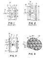
- Fig. 1 An example of such a screen is shown in Fig. 1, wherein the x-ray imaging screen 10 comprises a phosphor layer 11 formed on a substrate 12 and a photosensitive film sheet 13 pressed against the phosphor side of the screen.
- the particle fluoresces thus emitting light rays relatively uniformly in all directions as indicated by the arrows in Fig. 1.
- Those light rays which exit the phospher layer through the right-hand surface 16 enter the light sensitive film 13 and expose the film emulsion.
- the film can then be processed using conventional developing techniques to bring out a permanent record of the x-ray image formed on the film.
- An advantage of this arrangement over the use of direct exposure of the film to the x-ray energy lies in the greater sensitivity of the screen achieved by suitable selection of the phosphor material with high atomic numbers to increase the x-ray absorption efficiency of the screen.
- Light collection efficiency of an arrangement of this type can be increased by sandwiching the phosphor layer between two sheets of film thus capturing the light rays that escape from both facial surfaces of the phosphor screen.
- the composite image is then created by superimposing the two films after development.
- Another known approach to increasing sensitivity is shown in the modified screen 10' of Fig. 2 wherein mirror 18 is positioned on the left-hand side of the screen opposite the film 13. The light rays which would normally exit from this non-film side of the phosphor layer 11 are reflected by the mirror 18 to the film. Rather than using a seperate mirror, the same effect may also be created by aluminizing the surface 12a of the phosphor substrate 12 prior to depositing the phosphor.
- Fig. 2 Although the mirrored arrangement of Fig. 2 has the advantage of improving the light collection efficiency and therefore the sensitivity of the screen, it has the disadvantage that resolution is degraded by virtue of the increased effective spot size d' resulting from the reflected light, as compared to the smaller spot size d in Fig. 1 which results solely from the direct light rays.
- U.S. Patent No. 4,912,333 discloses only the use of lenslets in the form of microbeads as the retro-reflective medium. Effective as they are for this purpose, they have certain deficiencies resulting from the fact that close packed beads inherently have voids therebetween that reduce the reflection efficiency. They also have bands around the outer circumference of each bead that do not act as reflectors.
- an x-ray imaging phosphor screen and a method of making a planar array corner cube surface which comprises the steps of forming a wafer of single crystal material, such as silicon, having a cubic lattice structure with the facial surface of the wafer oriented in a ⁇ 111 ⁇ plane of the cubic structure, forming on the facial surface of the wafer a photoresist pattern of an array of equilateral triangle openings, the sides of the triangle openings being parallel to the ⁇ 110> directions of the cubic lattice in said ⁇ 111 ⁇ plane of the facial surface of the cubic structure, the parallel sides of adjacent triangle openings being spaced apart by a predetermined amount throughout the array pattern and etching said crystal material with an anisotropic etchant adapted to preferentially etch ⁇ 100 ⁇ planes of the cubic lattice structure to form a corresponding array of internal corner cu
- a retro-reflective sheet suitable for use as a back reflector for an x-ray stimulable phosphor imaging screen may be produced by forming a negative master of the corner cube surface, as by metal plating, and separating the negative master from the single crystal surface. A sheet having a planar array corner cube surface matching that of the etched crystal is then formed on the negative master, as by any molding process. After removal of the sheet from the negative master, the corner cube surface is made reflective by any suitable means such as evaporation of aluminum onto the surface.
- Figs. 1 and 2 effectively illustrate the dilemma between light collection efficiency and image resolution when a planar mirror surface is used to increase efficiency of the phosphor screen by reflecting light rays that would otherwise be lost to the photosensitive film.
- the mirror 18 in Fig. 2 reflects the fluorescent light rays outward thus significantly increasing the area of the spot size d' on the film 13 as compared to spot size d in the screen of Fig. 1.
- FIG. 3 A presently preferred embodiment of the imaging screen of the invention is illustrated in Fig. 3, wherein the planar mirror 18 of Fig. 2 is replaced by a sheet 20 having a corner cube retro-reflective surface 21 positioned facing the facial surface 22 of the phosphor layer 11.
- sheet 20 is positioned in contact with the outer surface of substrate 12 on which the phosphor layer 11 is deposited.
- the phosphor layer 11 may be deposited directly on sheet 20 thus eliminating the intermediate substrate 12.
- the drawings are not to scale, but are drawn so as to best illustrate the concepts involved.
- the materials used for fabrication of the retro-reflective sheet preferably should be substantially transparent to the x-radiation to be detected so as to allow penetration of the x-rays into the phosphor layer 11.
- Retro-reflective surfaces are known to exhibit the characteristic of reflecting incident light back substantially along an axis parallel to the axis of the incident light illumination as shown by double arrow 17.
- a corner cube retro-reflector surface As is known, a corner cube retro-reflector surface, best seen in Fig. 4, consists of a planar array of three-sided, interior pyramidal surfaces such as would be formed by the intersection of the corner of a cube by a plane normal to a line joining diametrically opposed corners of the cube.
- each interior pyramidal surface is formed by base lines 31a-31c lying in the plane of the paper and defining an open equilateral triangular aperture and by three planar sides 32a-32c defining isosceles triangle surfaces meeting at a common apex 23 positioned below the plane of the paper.
- These interior pyramidal surfaces are coated with a suitable reflective surface treatment, e.g. by aluminizing, to form the desired retro-reflective surface 21 (Fig. 3).
- the aperture of the reflector cell ideally should be very small in comparison to the distance of the light source from the aperture in order to preserve the desired resolution in the image created on film 13.
- the distance from the light source to the retro-reflective surface is dependent on the distance the x-ray penetrates into the phosphor layer before it is absorbed thereby creating a fluorescent event (plus the thickness of the phosphor substrate, if one is employed between the phosphor layer and the reflector surface).
- a thicker phosphor layer would increase the absorption efficiency of the screen and simultaneously increase the mean distance of phosphor events from the retroreflector surface, the maximum thickness is constrained by light scatter considerations which can degrade image resolution. Fluorescent events occurring remote from the film layer, corresponding to minimal x-ray penetration of the phosphor layer, inherently create a larger diameter spot on the film than events occurring close to the film layer. For typical x-ray phosphor compositions, a thickness range of from 50 microns to 200 microns is generally considered acceptable.
- the aperture of the reflector cell is about 50 microns, or smaller, as measured along an orthogonal line extending from one of the baselines 31a-31c to the corresponding opposite apex lying in the plane of the paper.
- the minimum aperture size is limited by the wavelength of the incident fluorescent light rays in order to avoid the effects of diffraction. For this reason, the minimum aperture size is about 10 ⁇ , where ⁇ is the wavelength of the incident light ray.
- a reflector cell aperture of about 5 microns would thus give preferred retro-reflection characteristics for screens of the type being considered, although larger aperture sizes up to about 50 microns should also work satisfactorily, as previously noted.
- a suitable corner cube reflector surface with apertures of this small size may be produced from single crystal cubic lattice silicon wafers which have been etched with an anisotropic etchant to produce a master pattern of corner cube reflector cells.
- an anisotropic etchant to produce a master pattern of corner cube reflector cells.
- the cube "abcdefgh” has six face planes, each of which can be specified by a set of three coordinates representing normalized intercepts of three mutually orthogonal reference axes.
- face “abcd” is represented in Miller indices within parentheses as the (100) plane and face “efgh” is represented as the ( 1 ⁇ 00) plane.
- All planes of equivalent symmetry can be represented by a single expression using curly brackets (braces) in place of the parentheses.
- curly brackets braces
- all cube face planes are represented by the expression ⁇ 100 ⁇ while all of the above-described canted planes of the cube can be represented by the expression ⁇ 111 ⁇ .
- Directions in a cube crystal are expressed in integers of a vector in the desired direction referred to the axis vectors and are written in square brackets [ ] to represent individual directions or in angled brackets ⁇ > to denote all directions of equivalent symmetry.
- the "x" axis "ea” is the [100] direction and the "-x” axis “ae” is the [ 1 ⁇ 00] direction.
- the line “af” in Fig. 5 is in the [ 1 ⁇ 01] direction while “fa” is in the [10 1 ⁇ ] direction.
- a full set of equivalent directions is thus expressed as ⁇ 110> with the subsets [ 1 ⁇ 01], [10 1 ⁇ ], [01 1 ⁇ ], [0 1 ⁇ 1], [1 1 ⁇ 0] and [ 11 ⁇ 0] being the directions of the three lines of intersection of the illustrated (111) plane in the cube faces. It will be appreciated that each of the equivalent symmetry planes ⁇ 111 ⁇ will have a corresponding subset of associated directions included within the expression ⁇ 111>.
- a wafer of single crystal material having cubic crystal symmetry preferably silicon
- a layer of photoresist material is then coated onto the facial surface of the wafer.
- a pattern of an array of close packed equilateral triangle openings is formed in the photoresist layer.
- the triangle openings are oriented in the pattern with the sides of each triangle parallel to the ⁇ 110> directions of the cube lattice structure lying in the ⁇ 111 ⁇ plane of the facial surface of the wafer and with parallel sides of adjacent triangle openings spaced apart by a predetermined amount as will be explained later.
- This physical arrangement may best be visualized with reference to the diagram of Fig. 6 which illustrates the geometric orientation of triangle openings 40 relative to the cubic lattice structure shown in Fig. 5.
- a layer of photoresist material 42 has formed therein a pattern of a close packed array of equilateral triangle openings 40.
- the sides of the triangle openings are oriented parallel to the ⁇ 110> directions of the cube lattice structure (lines ag, gf, and fa in Fig. 5) lying in the ⁇ 111 ⁇ plane of the facial surface of the single cube silicon wafer 44 (Fig. 7) on which the layer of photoresist material is deposited.
- a silicon wafer is produced with a reference edge cut in one side of the wafer to indicate the cube lattice orientation of the wafer.
- This reference edge can be specified to be cut parallel to a ⁇ 110> direction to indicate the desired physical orientation of the wafer relative to the crystal axes.
- a corresponding reference edge is incorporated in the mask parallel to a triangle side which may then be aligned with the reference edge of the wafer to assure proper alignment of the mask on the photoresist layer to achieve parallelism between the triangle openings and the ⁇ 110> directions of the cube lattice structure.
- FIG. 7 illustrates schematically the stages of development of the corner cube pattern beginning with the deposition of photoresist layer 42 on the silicon wafer 44.
- a plurality of properly oriented triangle openings 40 are formed in the photoresist layer 42.
- An anisotropic etchant selected to preferentially etch ⁇ 100 ⁇ planes of the cubic lattice structure of the silicon wafer 44 is then flowed in a known manner over the surface to the photoresist pattern to begin anisotropic etching of the ⁇ 100 ⁇ planes 32a-32c.
- etchants to achieve anisotropic etching of ⁇ 100 ⁇ planes in silicon are described in the book Integrated Circuit Fabrication Technology by David J. Elliott and published by McGraw-Hill Book Company, 1982, on pages 248-250.
- etching commences along the ⁇ 100 ⁇ planes 32a-32c, as represented by arrows 45 in Fig 7c, the process continues along the selected ⁇ 100 ⁇ planes with an increasing cavity size as the ⁇ 111 ⁇ plane surface 46 gradually decreases in each created cell.
- the process is completed when the ⁇ 111 ⁇ plane is fully depleted and the ⁇ 100 ⁇ planes 31a-31c meet at apex 23.
- the spacing between adjacent parallel sides of the triangle openings in the photoresist pattern is determined relative to the etch rate of the chosen etchant to allow the ⁇ 100 ⁇ planes of adjacent corner cubes to meet at the baselines of intersection 31a-31c corresponding to the ⁇ 110> directions in the facial surface of wafer 44 at least by the time the anisotropic etching of the corner cube is completed.
- the photoresist material 42 is washed off the silicon in known manner to thus leave the desired corner cube surface.
- the resulting corner cube surface on the face of wafer 44 may then serve as a pattern to form a negative master by plating a metal on the wafer which may then be separated from the wafer by peeling apart or dissolving the silicon.
- This metal master can then be coated with a suitable material such as is used in making film substrates to create the corner cube sheet 20 of Fig. 4 which, after hardening and removal, can be reflectorized, for example by evaporation of aluminum on the corner cube surface of the sheet.
- silicon wafers are produced in relatively small dimensions, typically in circular wafers of about six inches in diameter.
- a plurality of silicon wafers cut to suitable square or rectangular dimensions can be etched to prepare the master corner cube surface after which the wafers may be abutted to create the desired size of sheet. Cutting of the wafers may be done before or after the etching process.
Landscapes
- Chemical & Material Sciences (AREA)
- Engineering & Computer Science (AREA)
- Crystallography & Structural Chemistry (AREA)
- Materials Engineering (AREA)
- Metallurgy (AREA)
- Organic Chemistry (AREA)
- Physics & Mathematics (AREA)
- General Engineering & Computer Science (AREA)
- High Energy & Nuclear Physics (AREA)
- Measurement Of Radiation (AREA)
- Conversion Of X-Rays Into Visible Images (AREA)
- Optical Elements Other Than Lenses (AREA)
Abstract
Description
- This invention relates to x-ray imaging screens of the type employing x-ray stimulable phosphors to generate light emissions which are then used to expose photosensitive films or light sensitive solid state sensors to generate the x-ray image.
- It is known to provide an x-ray imaging screen in which a layer of phosphor is used to intercept x-rays in, for example, the 15-115 keV energy range to generate photoemissions which are then used to expose a photosensitive film or a light sensitive solid state sensor to generate the desired x-ray image.
- An example of such a screen is shown in Fig. 1, wherein the
x-ray imaging screen 10 comprises aphosphor layer 11 formed on asubstrate 12 and aphotosensitive film sheet 13 pressed against the phosphor side of the screen. When a bundle ofx-ray energy 14 enters the phosphor layer and is absorbed by aphosphor particle 15, the particle fluoresces thus emitting light rays relatively uniformly in all directions as indicated by the arrows in Fig. 1. Those light rays which exit the phospher layer through the right-hand surface 16 enter the lightsensitive film 13 and expose the film emulsion. The film can then be processed using conventional developing techniques to bring out a permanent record of the x-ray image formed on the film. An advantage of this arrangement over the use of direct exposure of the film to the x-ray energy lies in the greater sensitivity of the screen achieved by suitable selection of the phosphor material with high atomic numbers to increase the x-ray absorption efficiency of the screen. - One disadvantage of this arrangement, however, is that only some percentage, less than 50 percent, of the total light emitted from the stimulated phosphor is directed at the film. Light rays directed parallel to the face of the phosphor layer or directed away from the film are lost, thus limiting the efficiency in the conversion of x-ray energy to light effective in sensitizing the film.
- Light collection efficiency of an arrangement of this type, and therefore overall sensitivity, can be increased by sandwiching the phosphor layer between two sheets of film thus capturing the light rays that escape from both facial surfaces of the phosphor screen. The composite image is then created by superimposing the two films after development. Another known approach to increasing sensitivity is shown in the modified screen 10' of Fig. 2 wherein
mirror 18 is positioned on the left-hand side of the screen opposite thefilm 13. The light rays which would normally exit from this non-film side of thephosphor layer 11 are reflected by themirror 18 to the film. Rather than using a seperate mirror, the same effect may also be created by aluminizing the surface 12a of thephosphor substrate 12 prior to depositing the phosphor. Although the mirrored arrangement of Fig. 2 has the advantage of improving the light collection efficiency and therefore the sensitivity of the screen, it has the disadvantage that resolution is degraded by virtue of the increased effective spot size d' resulting from the reflected light, as compared to the smaller spot size d in Fig. 1 which results solely from the direct light rays. - In U.S. Patent No. 4,912,333, issued March 27, 1990, co-owned by the assignee of the present invention, it is suggested that light collection efficiency of a phosphor x-ray image intensifying screen can be improved by using a retro-reflective lenslets as the reflecting medium. A retro-reflective surface has the characteristic of reflecting incident light rays along an axis of reflection that is substantially parallel with the axis of the incident light ray. Because of this, the resultant illuminated spot size on the film is effectively the same as the spot size d in Fig. 1 created by the direct light rays, however with a greater intensity. Consequently, the use of a retro-reflector surface can increase the sensitivity of the imaging screen without a significant degradation of resolution in the image.
- While recognizing the advantage of a retro-reflector surface in x-ray intensifying screens, U.S. Patent No. 4,912,333 discloses only the use of lenslets in the form of microbeads as the retro-reflective medium. Effective as they are for this purpose, they have certain deficiencies resulting from the fact that close packed beads inherently have voids therebetween that reduce the reflection efficiency. They also have bands around the outer circumference of each bead that do not act as reflectors.
- It is therefore an object of the present invention to provide an x-ray stimulable phosphor imaging screen employing a retro-reflective back surface to enhance sensitivity but without experiencing the significant loss of resolution incurred with planar reflection surfaces.
- It is a further object of the invention to provide an imaging screen of the type described with a corner cube retro-reflector surface in which the corner cube apertures are microscopically small so as to be effective as a retro-reflector with light sources originating within relatively thin phosphor layers.
- It is yet another object of the invention to provide a method of forming a surface with an array of microscopically small corner cubes.
- It is still a further object of the invention to provide a method of making a sheet of retro-reflective material suitable for use in an x-ray stimulable phosphor imaging screen.
- According to the present invention, there is provided an x-ray imaging phosphor screen and method of making it as defined in
Claims 1 and 6. Essentially, there is provided an x-ray imaging phosphor screen and a method of making a planar array corner cube surface which comprises the steps of forming a wafer of single crystal material, such as silicon, having a cubic lattice structure with the facial surface of the wafer oriented in a {111} plane of the cubic structure, forming on the facial surface of the wafer a photoresist pattern of an array of equilateral triangle openings, the sides of the triangle openings being parallel to the <110> directions of the cubic lattice in said {111} plane of the facial surface of the cubic structure, the parallel sides of adjacent triangle openings being spaced apart by a predetermined amount throughout the array pattern and etching said crystal material with an anisotropic etchant adapted to preferentially etch {100} planes of the cubic lattice structure to form a corresponding array of internal corner cube pyramidal surfaces under the triangle openings of the photoresist pattern. At the completion of the etching step, the photoresist is removed to leave a planar array corner cube surface on the wafer facial surface. - Having created the planar array corner cube surface, a retro-reflective sheet suitable for use as a back reflector for an x-ray stimulable phosphor imaging screen may be produced by forming a negative master of the corner cube surface, as by metal plating, and separating the negative master from the single crystal surface. A sheet having a planar array corner cube surface matching that of the etched crystal is then formed on the negative master, as by any molding process. After removal of the sheet from the negative master, the corner cube surface is made reflective by any suitable means such as evaporation of aluminum onto the surface.
- In the drawings:
- Fig. 1 is a schematic cross section of a prior art form of x-ray stimulable phosphor imaging screen.
- Fig. 2 is a schematic cross section of another prior art form of x-ray stimulable phosphor imaging screen.
- Fig. 3 is a schematic cross section of an x-ray stimulable phosphor imaging screen produced in accordance with the present invention.
- Fig. 4 is a plan view of a portion of a corner cube retro-reflector surface produced in accordance with the present invention and embodied in the imaging screen of Fig. 3.
- Fig. 5 is a isometric diagram of a cube lattice useful in explaining the method and structure of the present invention.
- Fig. 6 is a plan view of a portion of a photoresist mask pattern used in the method of the present invention.
- Fig. 7 is a series of cross sectional views of a segment of a corner cube master panel illustrating the method of the invention.
- As previously discussed, Figs. 1 and 2 effectively illustrate the dilemma between light collection efficiency and image resolution when a planar mirror surface is used to increase efficiency of the phosphor screen by reflecting light rays that would otherwise be lost to the photosensitive film. The
mirror 18 in Fig. 2 reflects the fluorescent light rays outward thus significantly increasing the area of the spot size d' on thefilm 13 as compared to spot size d in the screen of Fig. 1. - A presently preferred embodiment of the imaging screen of the invention is illustrated in Fig. 3, wherein the
planar mirror 18 of Fig. 2 is replaced by asheet 20 having a corner cube retro-reflective surface 21 positioned facing thefacial surface 22 of thephosphor layer 11. In the illustrated embodiment,sheet 20 is positioned in contact with the outer surface ofsubstrate 12 on which thephosphor layer 11 is deposited. Alternatively, thephosphor layer 11 may be deposited directly onsheet 20 thus eliminating theintermediate substrate 12. It should be understood that the drawings are not to scale, but are drawn so as to best illustrate the concepts involved. It will also be appreciated that the materials used for fabrication of the retro-reflective sheet preferably should be substantially transparent to the x-radiation to be detected so as to allow penetration of the x-rays into thephosphor layer 11. - Retro-reflective surfaces are known to exhibit the characteristic of reflecting incident light back substantially along an axis parallel to the axis of the incident light illumination as shown by
double arrow 17. The smaller the aperture of the corner cube reflecting cell, the more nearly the incident and reflecting axis will be coincident. Accordingly, by virtue of the retro-reflective characteristic ofreflector sheet 20, the light rays that would normally exit from the left-handfacial surface 22 ofphosphor layer 11 or that would be reflected outward over an expanding area by a planar mirror surface, instead, are reflected back effectively along an axis passing through theoriginal light source 15 and thus serve to reinforce the exposure onfilm 13 with substantially the same spot size d as is realized with the unmodified screen of Fig. 1 except with a greater brightness. Thus sensitivity of the screen is improved without significant loss of resolution. - As is known, a corner cube retro-reflector surface, best seen in Fig. 4, consists of a planar array of three-sided, interior pyramidal surfaces such as would be formed by the intersection of the corner of a cube by a plane normal to a line joining diametrically opposed corners of the cube. Thus in Fig. 4, each interior pyramidal surface is formed by base lines 31a-31c lying in the plane of the paper and defining an open equilateral triangular aperture and by three
planar sides 32a-32c defining isosceles triangle surfaces meeting at acommon apex 23 positioned below the plane of the paper. These interior pyramidal surfaces are coated with a suitable reflective surface treatment, e.g. by aluminizing, to form the desired retro-reflective surface 21 (Fig. 3). - It is the nature of retro-reflector surfaces that the farther away the light source is from the plane of the array of reflector surfaces, the more the reflected light is truly retro-reflective with minimum reflective light scatter occurring. Stated another way, the aperture of the reflector cell ideally should be very small in comparison to the distance of the light source from the aperture in order to preserve the desired resolution in the image created on
film 13. In phosphor screens of the type contemplated by the present invention, the distance from the light source to the retro-reflective surface is dependent on the distance the x-ray penetrates into the phosphor layer before it is absorbed thereby creating a fluorescent event (plus the thickness of the phosphor substrate, if one is employed between the phosphor layer and the reflector surface). While a thicker phosphor layer would increase the absorption efficiency of the screen and simultaneously increase the mean distance of phosphor events from the retroreflector surface, the maximum thickness is constrained by light scatter considerations which can degrade image resolution. Fluorescent events occurring remote from the film layer, corresponding to minimal x-ray penetration of the phosphor layer, inherently create a larger diameter spot on the film than events occurring close to the film layer. For typical x-ray phosphor compositions, a thickness range of from 50 microns to 200 microns is generally considered acceptable. - For fluorescent events occurring in phosphor layers within this range of thickness, adequate retro-reflection can be achieved if the aperture of the reflector cell is about 50 microns, or smaller, as measured along an orthogonal line extending from one of the baselines 31a-31c to the corresponding opposite apex lying in the plane of the paper. The minimum aperture size, however, is limited by the wavelength of the incident fluorescent light rays in order to avoid the effects of diffraction. For this reason, the minimum aperture size is about 10λ, where λ is the wavelength of the incident light ray. Assuming a typical wavelength λ of about 0.5 micron, a reflector cell aperture of about 5 microns would thus give preferred retro-reflection characteristics for screens of the type being considered, although larger aperture sizes up to about 50 microns should also work satisfactorily, as previously noted.
- A suitable corner cube reflector surface with apertures of this small size may be produced from single crystal cubic lattice silicon wafers which have been etched with an anisotropic etchant to produce a master pattern of corner cube reflector cells. To aid in understanding the description of this process, it will be helpful to review the well known convention of Miller indices for describing three dimensional crystalline lattice structure and, more particularly, as applied to the specific example of a cube lattice.
- Referring to Fig. 5, the cube "abcdefgh" has six face planes, each of which can be specified by a set of three coordinates representing normalized intercepts of three mutually orthogonal reference axes. Thus face "abcd" is represented in Miller indices within parentheses as the (100) plane and face "efgh" is represented as the (


- All planes of equivalent symmetry can be represented by a single expression using curly brackets (braces) in place of the parentheses. Thus all cube face planes are represented by the expression {100} while all of the above-described canted planes of the cube can be represented by the expression {111}.
- Directions in a cube crystal are expressed in integers of a vector in the desired direction referred to the axis vectors and are written in square brackets [ ] to represent individual directions or in angled brackets < > to denote all directions of equivalent symmetry. In the cube of Fig. 5, the "x" axis "ea" is the [100] direction and the "-x" axis "ae" is the [


- Considering now the process by which a corner cube retro-reflector surface is prepared according to the present invention, a wafer of single crystal material having cubic crystal symmetry, preferably silicon, is formed to have a planar facial surface oriented in a {111} plane of the cubic lattice structure. A layer of photoresist material is then coated onto the facial surface of the wafer. Using known lithographic techniques, a pattern of an array of close packed equilateral triangle openings is formed in the photoresist layer. The triangle openings are oriented in the pattern with the sides of each triangle parallel to the <110> directions of the cube lattice structure lying in the {111} plane of the facial surface of the wafer and with parallel sides of adjacent triangle openings spaced apart by a predetermined amount as will be explained later. This physical arrangement may best be visualized with reference to the diagram of Fig. 6 which illustrates the geometric orientation of
triangle openings 40 relative to the cubic lattice structure shown in Fig. 5. - In Fig. 6, a layer of
photoresist material 42 has formed therein a pattern of a close packed array ofequilateral triangle openings 40. The sides of the triangle openings are oriented parallel to the <110> directions of the cube lattice structure (lines ag, gf, and fa in Fig. 5) lying in the {111} plane of the facial surface of the single cube silicon wafer 44 (Fig. 7) on which the layer of photoresist material is deposited. Typically, a silicon wafer is produced with a reference edge cut in one side of the wafer to indicate the cube lattice orientation of the wafer. This reference edge can be specified to be cut parallel to a <110> direction to indicate the desired physical orientation of the wafer relative to the crystal axes. Thus when the lithographic mask of equilateral triangles is produced, a corresponding reference edge is incorporated in the mask parallel to a triangle side which may then be aligned with the reference edge of the wafer to assure proper alignment of the mask on the photoresist layer to achieve parallelism between the triangle openings and the <110> directions of the cube lattice structure. Because of the rotational symmetry of the triangle pattern and the <110> directions in the {111} of the wafer face, it is only necessary for the reference edge of the mask to be parallel with a single triangle edge to achieve the desired orientation of the triangle openings with the cube lattice structure. - Referring now to Fig. 7, the process by which the desired corner cube pattern is etched in the silicon wafer will be considered. Fig. 7 illustrates schematically the stages of development of the corner cube pattern beginning with the deposition of
photoresist layer 42 on thesilicon wafer 44. After development of the photoresist with the triangle array mask as described above, a plurality of properly orientedtriangle openings 40 are formed in thephotoresist layer 42. An anisotropic etchant selected to preferentially etch {100} planes of the cubic lattice structure of thesilicon wafer 44 is then flowed in a known manner over the surface to the photoresist pattern to begin anisotropic etching of the {100} planes 32a-32c. Suitable etchants to achieve anisotropic etching of {100} planes in silicon are described in the book Integrated Circuit Fabrication Technology by David J. Elliott and published by McGraw-Hill Book Company, 1982, on pages 248-250. Once etching commences along the {100} planes 32a-32c, as represented byarrows 45 in Fig 7c, the process continues along the selected {100} planes with an increasing cavity size as the {111}plane surface 46 gradually decreases in each created cell. Eventually, the process is completed when the {111} plane is fully depleted and the {100} planes 31a-31c meet atapex 23. In order to produce x-ray imaging screens, it is desirable to create the corner cube array in such a manner that no residual {111} plane surface remains between adjacent corner cubes. To achieve this result, the spacing between adjacent parallel sides of the triangle openings in the photoresist pattern is determined relative to the etch rate of the chosen etchant to allow the {100} planes of adjacent corner cubes to meet at the baselines of intersection 31a-31c corresponding to the <110> directions in the facial surface ofwafer 44 at least by the time the anisotropic etching of the corner cube is completed. At the completion of the etching process, thephotoresist material 42 is washed off the silicon in known manner to thus leave the desired corner cube surface. - The resulting corner cube surface on the face of
wafer 44 may then serve as a pattern to form a negative master by plating a metal on the wafer which may then be separated from the wafer by peeling apart or dissolving the silicon. This metal master can then be coated with a suitable material such as is used in making film substrates to create thecorner cube sheet 20 of Fig. 4 which, after hardening and removal, can be reflectorized, for example by evaporation of aluminum on the corner cube surface of the sheet. - At the present time, silicon wafers are produced in relatively small dimensions, typically in circular wafers of about six inches in diameter. In order to make a corner cube sheet large enough to be used for producing x-ray imaging screens, a plurality of silicon wafers cut to suitable square or rectangular dimensions can be etched to prepare the master corner cube surface after which the wafers may be abutted to create the desired size of sheet. Cutting of the wafers may be done before or after the etching process.
- The invention has thus been described in detail with particular reference to a presently preferred embodiment, but it will be understood that variations and modifications can be effected within the scope of the invention as claimed.
Claims (10)
- An x-ray imaging phosphor screen employing x-ray stimulable phosphors to generate light emission which are used to expose photosensitive films (13) or light sensitive solid state sensors to generate an x-ray image; said phosphor screen comprising a phosphor layer (11) and reflective means (18; 20), wherein said reflective means is positioned in contact with an outer surface of a substrate (12) on which said phosphor layer (11) is deposited facing the facial surface (12a,22) of said phosphor layer opposite a side of said phosphor layer where the film is pressed against for exposure; characterized in thatthe reflective means (20) consists of a sheet having a corner cube surface coated with a light reflective surface treatment to form a retro-reflective surface (21) positioned facing said facial surface (22) of said phosphor layer (11) so as to form a retro-reflector with light sources (15) originating within the phosphor layer.
- The x-ray imaging phosphor screen of Claim 1 wherein the corner cubes of said retro-reflective surface (21) have an aperture size which is between 50 microns (1.27mm) in maximum and about ten times the wavelength of the incident light ray in minimum for a phosphor layer having a thickness range from 1.27mm (50 microns) to 5.08mm (200 microns) so that an incident and a reflecting axis of the x-rays will be coincident
- The x-ray imaging phosphor screen of Claim 1 or 2 wherein said corner cube retro-reflective surface (21) consists of a planar array of three-sided, interior pyramidal surfaces formed by intersection of the corner of a cube by a plane normal to a line joining diametrically opposed corners of the cube.
- The x-ray imaging phosphor screen of Claim 3 wherein each interior pyramidal surface is formed by base lines (31a, 31b, 31c) lying in said plane and defining said aperture as an open equilateral triangular aperture and by three planar sides (32a, 32b, 32c) defining isosceles triangle surfaces meeting at a common apex (23) positioned below said plane of said sheet (20) facing said facial surface (22).
- The x-ray imaging phosphor screen of Claim 1, 2 or 4 wherein said sheet (20) and said retro-reflective surface (21), respectively, are substantially transparent to the x-ray radiation to be detected so as to allow penetration of the x-rays into the phosphor layer (11).
- A method of making an x-ray imaging phosphor screen comprising the steps of:forming a wafer (44) of single crystal material having a cubic lattice structure with the facial surface of the wafer oriented in a {111} plane of the cubic structure;forming on the facial surface of the wafer a photoresist (42) pattern of an ordered array of closely spaced equilateral openings (40) wherein adjacent openings have paired, coextensive, parallel sides, the sides of the triangle openings being parallel to the <110> directions of the cubic lattice in said {111} plane of the facial surface of the cubic structure, and said parallel sides of adjacent openings being spaced apart by a predetermined amount throughout the array pattern;etching said crystal material with an anisoptropic etchant adapted to preferentially etch {100} planes of the cubic lattice structure to form a corresponding array of internal cube pyramidal surfaces under the openings of the photoresist pattern; andremoving the photoresist pattern to leave a planar array cube surface on a wafer facial surface; that method is characterized by the steps of:forming a negative structure from the planar array cube surface;forming a sheet (20) having sufficient thickness of substantially x-ray transparent material on the negative structure with a complete positive duplicate of the planar array cube surface formed on one face of the sheet;separating the sheet from the negative structure;coating the corner cube surface of the sheet with substantially x-ray transparent, light reflective material to form a cube retro-reflective surface (21);forming a layer (11) of x-ray absorbing, light emitting phosphor; andpositioning said sheet face-to-face against the phophor layer with the cube retro-reflective surface facing the phophor layer.
- The method of Claim 6 in which said photoresist pattern is formed as an array of closely spaced equilateral triangle openings (40); andan array of internal corner cube pyramidal surfaces is formed under the triangle openings of the photoresist pattern so that substantially no residual {111} plane surface remains between adjacent corner cubes.
- The method of Claim 7 in which said paired, coextensive, parallel sides of adjacent triangle openings are spaced equidistantly apart throughout the array pattern.
- The method of Claim 6 in which the wafer (44) is single cube silicon.
- The method of Claim 8 or 9 in which the spacing between said paired, coextensive, parallel sides of adjacent triangle openings is adapted to allow {100} planes of adjacent corner cubes to meet at least by the time anisotropic etching of the corner cubes is completed.
Applications Claiming Priority (3)
| Application Number | Priority Date | Filing Date | Title |
|---|---|---|---|
| US403246 | 1989-09-05 | ||
| US07/403,246 US4992699A (en) | 1989-09-05 | 1989-09-05 | X-ray phosphor imaging screen and method of making same |
| PCT/US1990/004911 WO1991003816A1 (en) | 1989-09-05 | 1990-08-29 | X-ray phosphor imaging screen and method of making same |
Publications (2)
| Publication Number | Publication Date |
|---|---|
| EP0441958A1 EP0441958A1 (en) | 1991-08-21 |
| EP0441958B1 true EP0441958B1 (en) | 1996-04-03 |
Family
ID=23595068
Family Applications (1)
| Application Number | Title | Priority Date | Filing Date |
|---|---|---|---|
| EP90914577A Expired - Lifetime EP0441958B1 (en) | 1989-09-05 | 1990-08-29 | X-ray phosphor imaging screen and method of making same |
Country Status (5)
| Country | Link |
|---|---|
| US (1) | US4992699A (en) |
| EP (1) | EP0441958B1 (en) |
| JP (1) | JP2892829B2 (en) |
| DE (1) | DE69026369T2 (en) |
| WO (1) | WO1991003816A1 (en) |
Families Citing this family (20)
| Publication number | Priority date | Publication date | Assignee | Title |
|---|---|---|---|---|
| US5753130A (en) * | 1992-05-15 | 1998-05-19 | Micron Technology, Inc. | Method for forming a substantially uniform array of sharp tips |
| US5391259A (en) * | 1992-05-15 | 1995-02-21 | Micron Technology, Inc. | Method for forming a substantially uniform array of sharp tips |
| US5416821A (en) * | 1993-05-10 | 1995-05-16 | Trw Inc. | Grid formed with a silicon substrate |
| CA2131243A1 (en) * | 1993-09-27 | 1995-03-28 | Kenneth R. Paulson | Process for forming a phosphor |
| US5695658A (en) * | 1996-03-07 | 1997-12-09 | Micron Display Technology, Inc. | Non-photolithographic etch mask for submicron features |
| WO1998056966A1 (en) * | 1997-06-12 | 1998-12-17 | Purdue Research Foundation | Corner cube arrays and manufacture thereof |
| US6461003B1 (en) | 1997-06-12 | 2002-10-08 | Purdue Research Foundation | Corner cube arrays and manufacture thereof |
| US6177236B1 (en) * | 1997-12-05 | 2001-01-23 | Xerox Corporation | Method of making a pixelized scintillation layer and structures incorporating same |
| US5981959A (en) * | 1997-12-05 | 1999-11-09 | Xerox Corporation | Pixelized scintillation layer and structures incorporating same |
| US6174449B1 (en) | 1998-05-14 | 2001-01-16 | Micron Technology, Inc. | Magnetically patterned etch mask |
| JP4053260B2 (en) * | 2000-10-18 | 2008-02-27 | シャープ株式会社 | Organic electroluminescence display element |
| KR100490816B1 (en) * | 2001-06-15 | 2005-05-24 | 샤프 가부시키가이샤 | Micro corner cube array, method of making the micro corner cube array and reflective type display device |
| JP3818906B2 (en) * | 2001-12-13 | 2006-09-06 | シャープ株式会社 | Micro corner cube array, manufacturing method thereof, and display device |
| JP2004086164A (en) * | 2002-06-27 | 2004-03-18 | Sharp Corp | Corner cube array and its fabricating method |
| US7201485B1 (en) | 2003-08-15 | 2007-04-10 | University Of South Florida | Corner cube retroreflector |
| JP4772102B2 (en) * | 2008-10-31 | 2011-09-14 | シャープ株式会社 | Corner cube array fabrication method |
| US9261301B2 (en) | 2013-05-28 | 2016-02-16 | M & M Electric Service, Inc. | Vehicle-transportable ice plant |
| CN105329847A (en) * | 2014-08-15 | 2016-02-17 | 中国科学院物理研究所 | Preparation method of micro-cavity structure array |
| JP6457099B2 (en) * | 2015-09-08 | 2019-01-23 | シャープ株式会社 | Wavelength conversion member and light emitting device |
| US11753991B2 (en) | 2019-06-25 | 2023-09-12 | Yantai Jereh Petroleum Equipment & Technologies Co., Ltd. | Intake-exhaust transport apparatus mobile power generation system and assembling method thereof |
Family Cites Families (9)
| Publication number | Priority date | Publication date | Assignee | Title |
|---|---|---|---|---|
| US2882413A (en) * | 1953-12-04 | 1959-04-14 | Vingerhoets Antonius Wilhelmus | Luminescent screen |
| US3944835A (en) * | 1974-09-25 | 1976-03-16 | General Electric Company | High energy radiation detector having improved reflective backing for phosphor layer |
| US4025662A (en) * | 1974-12-05 | 1977-05-24 | The United States Of America As Represented By The Secretary Of The Army | Method for making ultra high resolution phosphor screens |
| JPS53120376A (en) * | 1977-03-30 | 1978-10-20 | Fujitsu Ltd | Production of semiconductor device |
| NL7806828A (en) * | 1978-06-26 | 1979-12-28 | Philips Nv | LUMINESCENCE SCREEN. |
| US4227942A (en) * | 1979-04-23 | 1980-10-14 | General Electric Company | Photovoltaic semiconductor devices and methods of making same |
| JPS5949141A (en) * | 1982-09-13 | 1984-03-21 | Shimadzu Corp | Input face of x-ray fluorescent multiplier tube |
| JPS5993000A (en) * | 1982-11-17 | 1984-05-29 | Yoshihiro Hamakawa | Substrate for manufacturing single crystal thin film |
| JPS59202100A (en) * | 1983-04-30 | 1984-11-15 | コニカ株式会社 | Radiation image conversion panel and manufacture thereof |
-
1989
- 1989-09-05 US US07/403,246 patent/US4992699A/en not_active Expired - Fee Related
-
1990
- 1990-08-29 JP JP2513712A patent/JP2892829B2/en not_active Expired - Lifetime
- 1990-08-29 DE DE69026369T patent/DE69026369T2/en not_active Expired - Fee Related
- 1990-08-29 WO PCT/US1990/004911 patent/WO1991003816A1/en active IP Right Grant
- 1990-08-29 EP EP90914577A patent/EP0441958B1/en not_active Expired - Lifetime
Also Published As
| Publication number | Publication date |
|---|---|
| JPH04501614A (en) | 1992-03-19 |
| WO1991003816A1 (en) | 1991-03-21 |
| EP0441958A1 (en) | 1991-08-21 |
| DE69026369T2 (en) | 1996-10-31 |
| JP2892829B2 (en) | 1999-05-17 |
| US4992699A (en) | 1991-02-12 |
| DE69026369D1 (en) | 1996-05-09 |
Similar Documents
| Publication | Publication Date | Title |
|---|---|---|
| EP0441958B1 (en) | X-ray phosphor imaging screen and method of making same | |
| EP0126564B1 (en) | Method for reproducing a radiation image | |
| EP0233497B1 (en) | Radiation image storage panel | |
| GB1567446A (en) | Method of texturizing the surface of a crystalline semiconductor material | |
| JPS60103310A (en) | Manufacture of micro fresnel lens | |
| US4231657A (en) | Light-reflection type pattern forming system | |
| KR970010364B1 (en) | Process for forming a phospher | |
| JPH07509325A (en) | Stepped lens with Fresnel surface structure made by lithography and manufacturing method | |
| JPS5969927A (en) | X-ray exposure device | |
| US3852133A (en) | Method of manufacturing x-ray image intensifier input phosphor screen | |
| Hector et al. | Simultaneous optimization of spectrum, spatial coherence, gap, feature bias, and absorber thickness in synchrotron‐based x‐ray lithography | |
| Ceglio et al. | Micro‐Fresnel zone plates for coded imaging applications | |
| US3295968A (en) | Light trapping filter and method of making | |
| Van Beek et al. | Nanoscale freestanding gratings for ultraviolet blocking filters | |
| CA2186258A1 (en) | Method for fabricating a pixelized phosphor | |
| US3953621A (en) | Process of forming cathode ray tube screens | |
| EP0256582A1 (en) | Method of producing a phosphor screen for a colour cathode ray tube | |
| JP3192533B2 (en) | Optical element manufacturing method | |
| JP2771084B2 (en) | ND filter for light intensity diaphragm device | |
| JPS60166900A (en) | Screen for x-ray photograph and manufacture thereof | |
| JPS63181426A (en) | System for lithography | |
| JPS61160935A (en) | X-ray exposure method | |
| JPS63190335A (en) | Lithographic device | |
| JPH0646623B2 (en) | Mask structure for lithography | |
| JPH03222249A (en) | Image tube |
Legal Events
| Date | Code | Title | Description |
|---|---|---|---|
| PUAI | Public reference made under article 153(3) epc to a published international application that has entered the european phase |
Free format text: ORIGINAL CODE: 0009012 |
|
| AK | Designated contracting states |
Kind code of ref document: A1 Designated state(s): DE FR GB |
|
| 17P | Request for examination filed |
Effective date: 19910831 |
|
| 17Q | First examination report despatched |
Effective date: 19931115 |
|
| GRAH | Despatch of communication of intention to grant a patent |
Free format text: ORIGINAL CODE: EPIDOS IGRA |
|
| GRAA | (expected) grant |
Free format text: ORIGINAL CODE: 0009210 |
|
| AK | Designated contracting states |
Kind code of ref document: B1 Designated state(s): DE FR GB |
|
| REF | Corresponds to: |
Ref document number: 69026369 Country of ref document: DE Date of ref document: 19960509 |
|
| ET | Fr: translation filed | ||
| PLBE | No opposition filed within time limit |
Free format text: ORIGINAL CODE: 0009261 |
|
| STAA | Information on the status of an ep patent application or granted ep patent |
Free format text: STATUS: NO OPPOSITION FILED WITHIN TIME LIMIT |
|
| 26N | No opposition filed | ||
| PGFP | Annual fee paid to national office [announced via postgrant information from national office to epo] |
Ref country code: GB Payment date: 19990702 Year of fee payment: 10 |
|
| PGFP | Annual fee paid to national office [announced via postgrant information from national office to epo] |
Ref country code: FR Payment date: 19990802 Year of fee payment: 10 |
|
| PGFP | Annual fee paid to national office [announced via postgrant information from national office to epo] |
Ref country code: DE Payment date: 19990831 Year of fee payment: 10 |
|
| PG25 | Lapsed in a contracting state [announced via postgrant information from national office to epo] |
Ref country code: GB Free format text: LAPSE BECAUSE OF NON-PAYMENT OF DUE FEES Effective date: 20000829 |
|
| GBPC | Gb: european patent ceased through non-payment of renewal fee |
Effective date: 20000829 |
|
| PG25 | Lapsed in a contracting state [announced via postgrant information from national office to epo] |
Ref country code: FR Free format text: LAPSE BECAUSE OF NON-PAYMENT OF DUE FEES Effective date: 20010430 |
|
| PG25 | Lapsed in a contracting state [announced via postgrant information from national office to epo] |
Ref country code: DE Free format text: LAPSE BECAUSE OF NON-PAYMENT OF DUE FEES Effective date: 20010501 |
|
| REG | Reference to a national code |
Ref country code: FR Ref legal event code: ST |