EP0438544B1 - Verfahren zur herstellung einer feldemitteranordnung mit automatischer gate-justierung - Google Patents
Verfahren zur herstellung einer feldemitteranordnung mit automatischer gate-justierung Download PDFInfo
- Publication number
- EP0438544B1 EP0438544B1 EP90907546A EP90907546A EP0438544B1 EP 0438544 B1 EP0438544 B1 EP 0438544B1 EP 90907546 A EP90907546 A EP 90907546A EP 90907546 A EP90907546 A EP 90907546A EP 0438544 B1 EP0438544 B1 EP 0438544B1
- Authority
- EP
- European Patent Office
- Prior art keywords
- layer
- photoresist
- field emitter
- depositing
- oxide
- Prior art date
- Legal status (The legal status is an assumption and is not a legal conclusion. Google has not performed a legal analysis and makes no representation as to the accuracy of the status listed.)
- Expired - Lifetime
Links
- 238000000034 method Methods 0.000 title claims abstract description 31
- 238000003491 array Methods 0.000 title description 10
- 229910052751 metal Inorganic materials 0.000 claims abstract description 65
- 239000002184 metal Substances 0.000 claims abstract description 65
- 229920002120 photoresistant polymer Polymers 0.000 claims abstract description 50
- 239000000758 substrate Substances 0.000 claims abstract description 27
- 238000001020 plasma etching Methods 0.000 claims abstract description 13
- QVGXLLKOCUKJST-UHFFFAOYSA-N atomic oxygen Chemical compound [O] QVGXLLKOCUKJST-UHFFFAOYSA-N 0.000 claims abstract description 7
- 239000001301 oxygen Substances 0.000 claims abstract description 7
- 229910052760 oxygen Inorganic materials 0.000 claims abstract description 7
- 238000005530 etching Methods 0.000 claims description 11
- VYZAMTAEIAYCRO-UHFFFAOYSA-N Chromium Chemical compound [Cr] VYZAMTAEIAYCRO-UHFFFAOYSA-N 0.000 claims description 10
- 229910052804 chromium Inorganic materials 0.000 claims description 10
- 239000011651 chromium Substances 0.000 claims description 10
- PCHJSUWPFVWCPO-UHFFFAOYSA-N gold Chemical compound [Au] PCHJSUWPFVWCPO-UHFFFAOYSA-N 0.000 claims description 7
- 229910052737 gold Inorganic materials 0.000 claims description 7
- 239000010931 gold Substances 0.000 claims description 7
- 229910021420 polycrystalline silicon Inorganic materials 0.000 claims description 5
- 229920005591 polysilicon Polymers 0.000 claims description 5
- MYMOFIZGZYHOMD-UHFFFAOYSA-N Dioxygen Chemical compound O=O MYMOFIZGZYHOMD-UHFFFAOYSA-N 0.000 claims description 4
- ZOKXTWBITQBERF-UHFFFAOYSA-N Molybdenum Chemical compound [Mo] ZOKXTWBITQBERF-UHFFFAOYSA-N 0.000 claims description 4
- 229910001882 dioxygen Inorganic materials 0.000 claims description 4
- 229910052750 molybdenum Inorganic materials 0.000 claims description 4
- 239000011733 molybdenum Substances 0.000 claims description 4
- 230000001105 regulatory effect Effects 0.000 claims description 4
- 238000000151 deposition Methods 0.000 claims 23
- NLKNQRATVPKPDG-UHFFFAOYSA-M potassium iodide Chemical compound [K+].[I-] NLKNQRATVPKPDG-UHFFFAOYSA-M 0.000 description 3
- -1 for example Substances 0.000 description 2
- 239000012212 insulator Substances 0.000 description 2
- 238000004519 manufacturing process Methods 0.000 description 2
- 239000010409 thin film Substances 0.000 description 2
- KRHYYFGTRYWZRS-UHFFFAOYSA-N Fluorane Chemical compound F KRHYYFGTRYWZRS-UHFFFAOYSA-N 0.000 description 1
- XUIMIQQOPSSXEZ-UHFFFAOYSA-N Silicon Chemical compound [Si] XUIMIQQOPSSXEZ-UHFFFAOYSA-N 0.000 description 1
- 238000013459 approach Methods 0.000 description 1
- 230000015572 biosynthetic process Effects 0.000 description 1
- 230000001413 cellular effect Effects 0.000 description 1
- 238000005229 chemical vapour deposition Methods 0.000 description 1
- 230000001276 controlling effect Effects 0.000 description 1
- 238000001312 dry etching Methods 0.000 description 1
- 230000005669 field effect Effects 0.000 description 1
- 239000010408 film Substances 0.000 description 1
- 229910000040 hydrogen fluoride Inorganic materials 0.000 description 1
- 229910001092 metal group alloy Inorganic materials 0.000 description 1
- 239000000203 mixture Substances 0.000 description 1
- 230000000704 physical effect Effects 0.000 description 1
- 239000012286 potassium permanganate Substances 0.000 description 1
- 229910052710 silicon Inorganic materials 0.000 description 1
- 239000010703 silicon Substances 0.000 description 1
- XLYOFNOQVPJJNP-UHFFFAOYSA-N water Substances O XLYOFNOQVPJJNP-UHFFFAOYSA-N 0.000 description 1
Images

Classifications
-
- H—ELECTRICITY
- H01—ELECTRIC ELEMENTS
- H01J—ELECTRIC DISCHARGE TUBES OR DISCHARGE LAMPS
- H01J9/00—Apparatus or processes specially adapted for the manufacture, installation, removal, maintenance of electric discharge tubes, discharge lamps, or parts thereof; Recovery of material from discharge tubes or lamps
- H01J9/02—Manufacture of electrodes or electrode systems
- H01J9/022—Manufacture of electrodes or electrode systems of cold cathodes
- H01J9/025—Manufacture of electrodes or electrode systems of cold cathodes of field emission cathodes
Definitions
- the present invention relates generally to field emitter arrays, and more particularly to a process for fabricating self-aligned micron-sized field emitter arrays.
- Field emitter arrays typically comprise a metal/insulator/metal film sandwich with a cellular array of holes through the upper metal and insulator layers, leaving the edges of the upper metal layer (which serves as an accelerator electrode) effectively exposed to the upper surface of the lower metal layer (which serves as an emitter electrode).
- a number of conically-shaped electron emitter elements are mounted on the lower metal layer and extend upwardly therefrom such that their respective tips are located in respective holes in the upper metal layer.
- the present invention fabricates the arrays in accordance with the following process steps.
- Substantially conical field emitter elements are formed on a surface of a substrate, after which a layer of oxide is deposited on the substrate surface and over the field emitter elements.
- a layer of metal is then deposited over the layer of oxide to form a gate metal layer.
- a layer of photoresist is then deposited over the gate metal layer.
- the layer of photoresist is then plasma etched in an oxygen atmosphere to cause portions of the photoresist above respective field emitter elements to be removed and thereby provide self-aligned holes in the photoresist over each of the field emitter elements.
- the exposed gate metal layer above the field emitter elements is then etched using the layer of photoresist as a mask.
- the photoresist layer is removed, and the layer of oxide is etched to expose the field emitter elements.
- further processing may be performed to provide a second oxide layer and an anode metal layer in field emission triode devices.
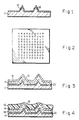
- FIGS. 1 and 2 show side and top views, respectively, of a substrate 11 having field emitter elements 12 formed on a surface of the substrate.
- the substrate 11 and the field emitter elements 12 may be of polysilicon, for example.
- the substrate 11 is fabricated in a conventional manner to provide an array of emitter elements thereon, with FIG. 2 showing a typical field emitter array.
- the substrate 11 and the field emitter elements 12 have a metal layer 20 disposed thereover.
- This metal layer 20 may be of molybdenum, for example.
- the metal layer 20 is typically deposited over elements 12 and substrate 11 to a thickness of from about 25 to about 20 nanometers (250 ⁇ to about 2000 ⁇ ), for example. It should be understood, however, that the metal layer 20 may be eliminated in some applications.
- a layer of oxide 13 is deposited over the surface of the substrate 11 and the field emitter elements 12 (or the metal layer 20 if it is employed).
- the oxide layer 13 is typically formed using a chemical vapor deposition process.
- the oxide layer 13 is deposited to a thickness of from about 500 to about 1500 nanometers (5000 ⁇ to about 15000 ⁇ ), for example.
- the chromium layer may have a thickness of from about 30 to about 100 nanometers (300 ⁇ to about 1000 ⁇ ), while the gold layer may have a thickness of from about 200 to about 500 nanometers (2000 ⁇ to about 5000 ⁇ ) for example.
- a layer of photoresist 15 is then deposited over the gate metal layer 14.
- the layer of photoresist 15 is typically deposited using a conventional spin-on procedure employing Hoechst AZ 1370 photoresist spun on at 4000 RPM for about 20 seconds, for example.
- FIG. 4 The structure of FIG. 4 is then processed to cause portions of the layer of photoresist 15 above respective field emitter elements 12 to be removed, as shown in FIG. 5, and thereby expose respective portions of the gate metal layer 14 above respective tip regions of the field emitter elements 12.
- This may be accomplished by plasma etching the layer of photoresist 15 in an oxygen environment.
- the plasma etching operation may be carried out in a plasma discharge stripping and etching system Model No. PDS/PDE-301 manufactured by LFE Corporation, Waltham, Massachusetts, for example.
- the aforementioned plasma discharge system may be initially evacuated to a pressure of about 13,33 Pa (0.1 torr), after which a regulated flow of oxygen gas may be passed through the system at a flow rate of about 240 cc per minute and at a pressure of about 399,9 Pa (3 torr) before commencement of the plasma discharge.
- a plasma discharge is then established in the system for a predetermined time to achieve the desired photoresist removal.
- precisely-aligned openings 16 are formed directly over respective field emitter elements 12 of the array.
- the size of the openings 16 may be controlled by appropriately controlling process parameters, including time and power setting of the plasma discharge apparatus and/or the initial thickness of the layer of photoresist 15.
- the field emitter elements 12 that have been exposed via openings 16 in the preceding step are then etched by means of a conventional etching procedure, for example, using the layer of photoresist 15 as a mask.
- a mixture of water and potassium iodide may be employed for a time duration of from about 1 minute to about 5 minutes to etch the gold, for example, and potassium permanganate for about 7 seconds, and oxalic for about 7 seconds may be employed to etch the chromium, for example.
- the layer of photoresist 15 is then removed, and the layer of oxide 13 is etched using a conventional etching procedure using buffered hydrogen fluoride, for example, to expose the field emitter elements 12. This results in a self-aligned cathode structure as shown in FIG. 8.
- FIGS. 9 and 10 additional processing steps are illustrated that enable fabrication of a self-aligned anode structure above the field emission cathode structure fabricated pursuant to the process of FIGS. 1-8.
- a second layer of oxide 17 is deposited on top of the gate metal layer 14, after which an additional layer of metal 18, which may serve as an anode metal layer in the resultant device, is deposited over the second layer of oxide 17.
- FIG. 9 is processed in a manner described above with respect to FIGS. 4-8.
- a layer of photoresist is applied to the top surface of the anode metal layer 18 and is then plasma etched to remove portions of the layer of photoresist above the elements 12.
- the anode metal layer 18 is then etched using the layer of photoresist as a mask.
- the layer of photoresist is then removed, and the first and second oxide layers 13,17 are etched to expose the field emitter elements 12, resulting in the structure shown in FIG. 10.
- the above-described embodiments are merely illustrative of some of the many specific embodiments utilizing the principles of the present invention.
- metal may be used instead of polysilicon to form the substrate and the emitter elements.
- dry etching of the oxide and metal layers may be employed where anisotropic etching is critical.
- the gate metal layer may be comprised of metal alloys other than chromium and gold, such as by molybdenum, for example.
Landscapes
- Engineering & Computer Science (AREA)
- Manufacturing & Machinery (AREA)
- Cold Cathode And The Manufacture (AREA)
- Electrodes Of Semiconductors (AREA)
Claims (13)
- Verfahren zur Herstellung einer Feldemitteranordnung, welches die Schritte aufweist:
Ausbilden von im wesentlichen konisch ausgebildeten Feldemitterelementen auf einer Oberfläche eines Substrats (11);
Abscheiden einer Schicht (13) aus Oxid über die Substratoberfläche und die Feldemitterelemente (12);
Abscheiden einer Schicht (14) aus Metall über die Schicht (13) aus Oxid zur Ausbildung einer Gatemetallschicht;
Abscheiden einer Schicht (15) aus Photolack über die Gatemetallschicht;
Plasmaätzen der Schicht (15) aus Photolack in einer Sauerstoffatmosphäre derart, daß Abschnitte des Photolackes oberhalb jeweiliger Feldemitterelemente (12) entfernt werden und hierdurch jeweilige Abschnitte der Gatemetallschicht oberhalb jeweiliger Spitzenbereiche der Feldemitterelemente (12) freigelegt werden;
Ätzen der freigelegten Abschnitte der Gatemetallschicht (14) unter Verwendung der Schicht (15) aus Photolack als eine Maske;
Entfernen der Schicht (15) aus Photolack; und
Ätzen der freigelegten Abschnitte der Schicht (13) aus Oxid zum Freilegen der Feldemitterelemente (12). - Verfahren nach Anspruch 1, bei dem das Substrat (11) und die Feldemitterelemente (12) aus Polysilizium hergestellt sind.
- Verfahren nach Anspruch 1, bei dem der Schritt des Abscheidens einer Schicht (14) aus Metall über die Schicht (13) aus Oxid die Schritte aufweist:
Abscheiden einer Schicht aus Chrom auf der Schicht (13) aus Oxid; und
Abscheiden einer Schicht aus Gold auf der Schicht aus Chrom. - Verfahren nach Anspruch 1, bei dem der Schritt des Plasmaätzens der Schicht (15) aus Photolack die Schritte aufweist:
Anordnen des Substrates in einer Plasmaentladungsvorrichtung;
Evakuieren der Vorrichtung bis zu einem vorbestimmten Druck;
Passieren eines geregelten Flusses von Sauerstoffgas über das Substrat; und
Einrichten einer Plasmaentladung in der Vorrichtung für eine vorbestimmte Zeit. - Verfahren zur Herstellung einer Feldemitteranordnung, welches die Schritte aufweist:
Ausbilden von im wesentlichen konisch ausgebildeten Feldemitterelementen auf einer Oberfläche eines Substrats (11);
Abscheiden einer ersten Schicht aus Metall (20) auf die Substratoberfläche und über die Feldemitterelemente (12);
Abscheiden einer Schicht (13) aus Oxid über die erste Schicht (20) aus Metall;
Abscheiden einer zweiten Schicht (14) aus Metall über die Schicht (13) aus Oxid zur Ausbildung einer Gatemetallschicht;
Abscheiden einer Schicht (15) aus Photolack über die Gatemetallschicht;
Plasmaätzen der Schicht (15) aus Photolack in einer Sauerstoffatmosphäre derart, daß Abschnitte des Photolackes oberhalb jeweiliger Feldemitterelemente (12) entfernt werden und hierdurch jeweilige Abschnitte der Gatemetallschicht oberhalb jeweiliger Spitzenbereiche der Feldemitterelemente (12) freigelegt werden;
Ätzen der freigelegten Abschnitte der Gatemetallschicht (14) unter Verwendung der Schicht (15) aus Photolack als eine Maske;
Entfernen der Schicht (15) aus Photolack; und
Ätzen der freigelegten Abschnitte der Schicht (13) aus Oxid zum Freilegen der Feldemitterelemente (12). - Verfahren nach Anspruch 5, bei dem das Substrat und die Feldemitterelemente aus Polysilizium hergestellt sind.
- Verfahren nach Anspruch 5, bei dem die erste Schicht aus Metall aus Molybdän hergestellt ist.
- Verfahren nach Anspruch 5, bei dem der Schritt des Abscheidens einer zweiten Schicht (14) aus Metall über die Schicht aus Oxid die Schritte aufweist:
Abscheiden einer Schicht aus Chrom auf der Schicht aus Oxid; und
Abscheiden einer Schicht aus Gold auf der Schicht aus Chrom. - Verfahren nach Anspruch 5, bei dem der Schritt des Plasmaätzens der Schicht (15) aus Photolack die Schritte aufweist:
Anordnen des Substrates in einer Plasmaentladungsvorrichtung;
Evakuieren der Vorrichtung bis zu einem vorbestimmten Druck;
Passieren eines geregelten Flusses von Sauerstoffgas über das Substrat; und
Einrichten einer Plasmaentladung in der Vorrichtung für eine vorbestimmte Zeit. - Verfahren zur Herstellung einer Feldemitteranordnung, welches die Schritte aufweist:
Ausbilden von im wesentlichen konisch ausgebildeten Feldemitterelementen (12) auf einer Oberfläche eines Substrats (11);
Abscheiden einer ersten Schicht (13) aus Oxid über die Substratoberfläche und die Feldemitterelemente (12);
Abscheiden einer Schicht (14) aus Metall über die Schicht (13) aus Oxid zur Ausbildung einer Gatemetallschicht;
Abscheiden einer ersten Schicht (15) aus Photolack über die Gatemetallschicht;
Plasmaätzen der ersten Schicht (15) aus Photolack in einer Sauerstoffatmosphäre derart, daß Abschnitte des Photolackes oberhalb jeweiliger Feldemitterelemente (12) entfernt werden und hierdurch jeweilige Abschnitte der Gatemetallschicht oberhalb jeweiliger Spitzenbereiche der Feldemitterelemente (12) freigelegt werden;
Ätzen der freigelegten Abschnitte der Gatemetallschicht (14) unter Verwendung der ersten Schicht (15) aus Photolack als eine Maske;
Entfernen der ersten Schicht (15) aus Photolack;
Abscheiden einer zweiten Schicht (17) aus Oxid über die Gatemetallschicht (14) und über jeweilige Abschnitte der ersten Oxidschicht (13), die nicht durch die Gatemetallschicht (14) bedeckt sind;
Abscheiden einer Schicht (18) aus Metall über die zweite Schicht (17) aus Oxid zur Ausbildung einer Anodenmetallschicht;
Abscheiden einer zweiten Schicht aus Photolack über die Anodenmetallschicht;
Plasmaätzen der zweiten Schicht aus Photolack in einer Sauerstoffatmosphäre, um Abschnitte des Photolackes in der zweiten Schicht oberhalb jeweiliger Feldemitterelemente (12) zu entfernen und dadurch jeweilige Abschnitte der Anodenmetallschicht (18) oberhalb jeweiliger Spitzenbereiche der Feldemitterelemente (12) freizulegen;
Ätzen der freigelegten Abschnitte der Anodenmetallschicht (18) unter Verwendung der zweiten Schicht aus Photolack als eine Maske; und
Ätzen der freigelegten Abschnitte der ersten und zweiten Schichten (13, 17) aus Oxid zum Freilegen der Feldemitterelemente. - Verfahren nach Anspruch 10, bei dem das Substrat und die Feldemitterelemente aus Polysilizium hergestellt sind.
- Verfahren nach Anspruch 11, bei dem der Schritt des Abscheidens einer Schicht aus Metall über die Schicht aus Oxid zur Ausbildung einer Gatemetallschicht die Schritte aufweist:
Abscheiden einer Schicht aus Chrom auf der Schicht aus Oxid; und
Abscheiden einer Schicht aus Gold auf der Schicht aus Chrom. - Verfahren nach Anspruch 10, bei dem die Schritte des Plasmaätzens der ersten und zweiten Schichten aus Photolack jeweils die Schritte aufweisen:
Anordnen des Substrates in einer Plasmaentladungsvorrichtung;
Evakuieren der Vorrichtung bis zu einem vorbestimmten Druck;
Passieren eines geregelten Flusses von Sauerstoffgas über das Substrat; und
Einrichten einer Plasmaentladung in der Vorrichtung für eine vorbestimmte Zeit.
Applications Claiming Priority (3)
| Application Number | Priority Date | Filing Date | Title |
|---|---|---|---|
| US393199 | 1989-08-14 | ||
| US07/393,199 US4943343A (en) | 1989-08-14 | 1989-08-14 | Self-aligned gate process for fabricating field emitter arrays |
| PCT/US1990/002184 WO1991003066A1 (en) | 1989-08-14 | 1990-04-23 | Self-aligned gate process for fabricating field emitter arrays |
Publications (2)
| Publication Number | Publication Date |
|---|---|
| EP0438544A1 EP0438544A1 (de) | 1991-07-31 |
| EP0438544B1 true EP0438544B1 (de) | 1995-01-25 |
Family
ID=23553689
Family Applications (1)
| Application Number | Title | Priority Date | Filing Date |
|---|---|---|---|
| EP90907546A Expired - Lifetime EP0438544B1 (de) | 1989-08-14 | 1990-04-23 | Verfahren zur herstellung einer feldemitteranordnung mit automatischer gate-justierung |
Country Status (6)
| Country | Link |
|---|---|
| US (1) | US4943343A (de) |
| EP (1) | EP0438544B1 (de) |
| CA (1) | CA2034481C (de) |
| DE (1) | DE69016397D1 (de) |
| IL (1) | IL94199A0 (de) |
| WO (1) | WO1991003066A1 (de) |
Families Citing this family (55)
| Publication number | Priority date | Publication date | Assignee | Title |
|---|---|---|---|---|
| GB9101723D0 (en) * | 1991-01-25 | 1991-03-06 | Marconi Gec Ltd | Field emission devices |
| US5312514A (en) * | 1991-11-07 | 1994-05-17 | Microelectronics And Computer Technology Corporation | Method of making a field emitter device using randomly located nuclei as an etch mask |
| US5281891A (en) * | 1991-02-22 | 1994-01-25 | Matsushita Electric Industrial Co., Ltd. | Electron emission element |
| US5181874A (en) * | 1991-03-26 | 1993-01-26 | Hughes Aircraft Company | Method of making microelectronic field emission device with air bridge anode |
| US5136205A (en) * | 1991-03-26 | 1992-08-04 | Hughes Aircraft Company | Microelectronic field emission device with air bridge anode |
| EP0525763B1 (de) * | 1991-08-01 | 1995-10-25 | Texas Instruments Incorporated | Verfahren zur Herstellung eines Mikroelektronisches Bauelement |
| EP0525764B1 (de) * | 1991-08-01 | 1995-11-02 | Texas Instruments Incorporated | Verfahren zur Bildung von Vacuummikrokammern zur Einbettung von Vorrichtungen der Mikroelektronik |
| US5270574A (en) * | 1991-08-01 | 1993-12-14 | Texas Instruments Incorporated | Vacuum micro-chamber for encapsulating a microelectronics device |
| US5536193A (en) * | 1991-11-07 | 1996-07-16 | Microelectronics And Computer Technology Corporation | Method of making wide band gap field emitter |
| US5199918A (en) * | 1991-11-07 | 1993-04-06 | Microelectronics And Computer Technology Corporation | Method of forming field emitter device with diamond emission tips |
| US5399238A (en) * | 1991-11-07 | 1995-03-21 | Microelectronics And Computer Technology Corporation | Method of making field emission tips using physical vapor deposition of random nuclei as etch mask |
| US5266530A (en) * | 1991-11-08 | 1993-11-30 | Bell Communications Research, Inc. | Self-aligned gated electron field emitter |
| US5199917A (en) * | 1991-12-09 | 1993-04-06 | Cornell Research Foundation, Inc. | Silicon tip field emission cathode arrays and fabrication thereof |
| US5627427A (en) * | 1991-12-09 | 1997-05-06 | Cornell Research Foundation, Inc. | Silicon tip field emission cathodes |
| US5318918A (en) * | 1991-12-31 | 1994-06-07 | Texas Instruments Incorporated | Method of making an array of electron emitters |
| US5229331A (en) * | 1992-02-14 | 1993-07-20 | Micron Technology, Inc. | Method to form self-aligned gate structures around cold cathode emitter tips using chemical mechanical polishing technology |
| US5696028A (en) * | 1992-02-14 | 1997-12-09 | Micron Technology, Inc. | Method to form an insulative barrier useful in field emission displays for reducing surface leakage |
| US5653619A (en) * | 1992-03-02 | 1997-08-05 | Micron Technology, Inc. | Method to form self-aligned gate structures and focus rings |
| US5259799A (en) * | 1992-03-02 | 1993-11-09 | Micron Technology, Inc. | Method to form self-aligned gate structures and focus rings |
| US5186670A (en) * | 1992-03-02 | 1993-02-16 | Micron Technology, Inc. | Method to form self-aligned gate structures and focus rings |
| US5659224A (en) * | 1992-03-16 | 1997-08-19 | Microelectronics And Computer Technology Corporation | Cold cathode display device |
| US5449970A (en) * | 1992-03-16 | 1995-09-12 | Microelectronics And Computer Technology Corporation | Diode structure flat panel display |
| US6127773A (en) * | 1992-03-16 | 2000-10-03 | Si Diamond Technology, Inc. | Amorphic diamond film flat field emission cathode |
| US5675216A (en) * | 1992-03-16 | 1997-10-07 | Microelectronics And Computer Technololgy Corp. | Amorphic diamond film flat field emission cathode |
| US5543684A (en) | 1992-03-16 | 1996-08-06 | Microelectronics And Computer Technology Corporation | Flat panel display based on diamond thin films |
| US5329207A (en) * | 1992-05-13 | 1994-07-12 | Micron Technology, Inc. | Field emission structures produced on macro-grain polysilicon substrates |
| US5499938A (en) * | 1992-07-14 | 1996-03-19 | Kabushiki Kaisha Toshiba | Field emission cathode structure, method for production thereof, and flat panel display device using same |
| US5382185A (en) * | 1993-03-31 | 1995-01-17 | The United States Of America As Represented By The Secretary Of The Navy | Thin-film edge field emitter device and method of manufacture therefor |
| US5584740A (en) * | 1993-03-31 | 1996-12-17 | The United States Of America As Represented By The Secretary Of The Navy | Thin-film edge field emitter device and method of manufacture therefor |
| DE59402800D1 (de) * | 1993-04-05 | 1997-06-26 | Siemens Ag | Verfahren zur Herstellung von Tunneleffekt-Sensoren |
| FR2709206B1 (fr) * | 1993-06-14 | 2004-08-20 | Fujitsu Ltd | Dispositif cathode ayant une petite ouverture, et son procédé de fabrication. |
| US5532177A (en) * | 1993-07-07 | 1996-07-02 | Micron Display Technology | Method for forming electron emitters |
| DE69422234T2 (de) * | 1993-07-16 | 2000-06-15 | Matsushita Electric Industrial Co., Ltd. | Verfahren zur Herstellung einer Feldemissionsanordnung |
| US5592736A (en) * | 1993-09-03 | 1997-01-14 | Micron Technology, Inc. | Fabricating an interconnect for testing unpackaged semiconductor dice having raised bond pads |
| US6414506B2 (en) | 1993-09-03 | 2002-07-02 | Micron Technology, Inc. | Interconnect for testing semiconductor dice having raised bond pads |
| US5483741A (en) * | 1993-09-03 | 1996-01-16 | Micron Technology, Inc. | Method for fabricating a self limiting silicon based interconnect for testing bare semiconductor dice |
| CN1134754A (zh) * | 1993-11-04 | 1996-10-30 | 微电子及计算机技术公司 | 制作平板显示系统和元件的方法 |
| US5445550A (en) * | 1993-12-22 | 1995-08-29 | Xie; Chenggang | Lateral field emitter device and method of manufacturing same |
| US5844251A (en) * | 1994-01-05 | 1998-12-01 | Cornell Research Foundation, Inc. | High aspect ratio probes with self-aligned control electrodes |
| JP3388870B2 (ja) * | 1994-03-15 | 2003-03-24 | 株式会社東芝 | 微小3極真空管およびその製造方法 |
| JPH0831308A (ja) | 1994-07-12 | 1996-02-02 | Nec Corp | 電界放出冷陰極の製造方法 |
| GB9415892D0 (en) * | 1994-08-05 | 1994-09-28 | Central Research Lab Ltd | A self-aligned gate field emitter device and methods for producing the same |
| US5504385A (en) * | 1994-08-31 | 1996-04-02 | At&T Corp. | Spaced-gate emission device and method for making same |
| US5669801A (en) * | 1995-09-28 | 1997-09-23 | Texas Instruments Incorporated | Field emission device cathode and method of fabrication |
| US5683282A (en) * | 1995-12-04 | 1997-11-04 | Industrial Technology Research Institute | Method for manufacturing flat cold cathode arrays |
| US5857884A (en) * | 1996-02-07 | 1999-01-12 | Micron Display Technology, Inc. | Photolithographic technique of emitter tip exposure in FEDS |
| US6022256A (en) * | 1996-11-06 | 2000-02-08 | Micron Display Technology, Inc. | Field emission display and method of making same |
| JP3524343B2 (ja) * | 1997-08-26 | 2004-05-10 | キヤノン株式会社 | 微小開口の形成方法と微小開口を有する突起、及びそれらによるプローブまたはマルチプローブ、並びに該プローブを用いた表面観察装置、露光装置、情報処理装置 |
| US6710539B2 (en) | 1998-09-02 | 2004-03-23 | Micron Technology, Inc. | Field emission devices having structure for reduced emitter tip to gate spacing |
| US6197607B1 (en) * | 1999-03-01 | 2001-03-06 | Micron Technology, Inc. | Method of fabricating field emission arrays to optimize the size of grid openings and to minimize the occurrence of electrical shorts |
| US6391670B1 (en) | 1999-04-29 | 2002-05-21 | Micron Technology, Inc. | Method of forming a self-aligned field extraction grid |
| KR100464314B1 (ko) | 2000-01-05 | 2004-12-31 | 삼성에스디아이 주식회사 | 전계방출소자 및 그 제조방법 |
| GB2383187B (en) * | 2001-09-13 | 2005-06-22 | Microsaic Systems Ltd | Electrode structures |
| CN102130122B (zh) * | 2010-01-20 | 2012-08-01 | 上海华虹Nec电子有限公司 | 锗硅异质结三极管的版图结构 |
| CN110104609A (zh) * | 2019-05-10 | 2019-08-09 | 中国科学院微电子研究所 | 一种微电极及其形成方法 |
Family Cites Families (9)
| Publication number | Priority date | Publication date | Assignee | Title |
|---|---|---|---|---|
| US3453478A (en) * | 1966-05-31 | 1969-07-01 | Stanford Research Inst | Needle-type electron source |
| US3755704A (en) * | 1970-02-06 | 1973-08-28 | Stanford Research Inst | Field emission cathode structures and devices utilizing such structures |
| US3665241A (en) * | 1970-07-13 | 1972-05-23 | Stanford Research Inst | Field ionizer and field emission cathode structures and methods of production |
| JPS5325632B2 (de) * | 1973-03-22 | 1978-07-27 | ||
| JPS5436828B2 (de) * | 1974-08-16 | 1979-11-12 | ||
| US3921022A (en) * | 1974-09-03 | 1975-11-18 | Rca Corp | Field emitting device and method of making same |
| US4307507A (en) * | 1980-09-10 | 1981-12-29 | The United States Of America As Represented By The Secretary Of The Navy | Method of manufacturing a field-emission cathode structure |
| US4513308A (en) * | 1982-09-23 | 1985-04-23 | The United States Of America As Represented By The Secretary Of The Navy | p-n Junction controlled field emitter array cathode |
| GB8720792D0 (en) * | 1987-09-04 | 1987-10-14 | Gen Electric Co Plc | Vacuum devices |
-
1989
- 1989-08-14 US US07/393,199 patent/US4943343A/en not_active Expired - Lifetime
-
1990
- 1990-04-23 EP EP90907546A patent/EP0438544B1/de not_active Expired - Lifetime
- 1990-04-23 WO PCT/US1990/002184 patent/WO1991003066A1/en not_active Ceased
- 1990-04-23 DE DE69016397T patent/DE69016397D1/de not_active Expired - Lifetime
- 1990-04-23 CA CA002034481A patent/CA2034481C/en not_active Expired - Fee Related
- 1990-04-25 IL IL94199A patent/IL94199A0/xx not_active IP Right Cessation
Also Published As
| Publication number | Publication date |
|---|---|
| WO1991003066A1 (en) | 1991-03-07 |
| EP0438544A1 (de) | 1991-07-31 |
| IL94199A0 (en) | 1991-01-31 |
| US4943343A (en) | 1990-07-24 |
| CA2034481C (en) | 1993-10-05 |
| CA2034481A1 (en) | 1991-02-15 |
| DE69016397D1 (de) | 1995-03-09 |
Similar Documents
| Publication | Publication Date | Title |
|---|---|---|
| US4943343A (en) | Self-aligned gate process for fabricating field emitter arrays | |
| US5151061A (en) | Method to form self-aligned tips for flat panel displays | |
| EP1018131B1 (de) | Gittergesteuerte elektronenemissionsvorrichtung und herstellungsverfahren dafür | |
| US4307507A (en) | Method of manufacturing a field-emission cathode structure | |
| US5702281A (en) | Fabrication of two-part emitter for gated field emission device | |
| US5150192A (en) | Field emitter array | |
| US5696385A (en) | Field emission device having reduced row-to-column leakage | |
| US5409568A (en) | Method of fabricating a microelectronic vacuum triode structure | |
| US6495955B1 (en) | Structure and method for improved field emitter arrays | |
| US6737793B2 (en) | Apparatus for emitting electrons comprising a subsurface emitter structure | |
| EP0876676A2 (de) | Feldemissionsvorrichtung und schutzschicht-verfahren zu deren derstellung | |
| US6057172A (en) | Field-emission cathode and method of producing the same | |
| US5607335A (en) | Fabrication of electron-emitting structures using charged-particle tracks and removal of emitter material | |
| US6403390B2 (en) | Method of fabricating field emission arrays to optimize the size of grid openings and to minimize the occurrence of electrical shorts | |
| JP2000173444A (ja) | 電界放出型冷陰極及びその製造方法 | |
| KR100186253B1 (ko) | Locos에 의한 실리콘 fea 제조방법 | |
| JPH04505073A (ja) | フィールドエミッタアレイの製造用の自己整列ゲート方法 | |
| KR100290136B1 (ko) | 전계방출소자제조방법 | |
| JPH05242797A (ja) | 電子放出素子の製造方法 | |
| JP2737675B2 (ja) | 縦型微小冷陰極の製造方法 | |
| JP3457054B2 (ja) | 棒状シリコン構造物の製造方法 | |
| KR100282261B1 (ko) | 전계방출 캐소드 어레이 및 이의 제조방법 | |
| JP2846988B2 (ja) | 電界放出型電子放出源素子 | |
| JPH11260247A (ja) | 電界放出素子並びにその形成方法及び利用 | |
| JPH04262337A (ja) | 電界放出陰極の製造方法 |
Legal Events
| Date | Code | Title | Description |
|---|---|---|---|
| PUAI | Public reference made under article 153(3) epc to a published international application that has entered the european phase |
Free format text: ORIGINAL CODE: 0009012 |
|
| AK | Designated contracting states |
Kind code of ref document: A1 Designated state(s): BE CH DE FR GB IT LI NL |
|
| 17P | Request for examination filed |
Effective date: 19910812 |
|
| 17Q | First examination report despatched |
Effective date: 19940121 |
|
| RAP1 | Party data changed (applicant data changed or rights of an application transferred) |
Owner name: HUGHES AIRCRAFT COMPANY |
|
| GRAA | (expected) grant |
Free format text: ORIGINAL CODE: 0009210 |
|
| AK | Designated contracting states |
Kind code of ref document: B1 Designated state(s): BE CH DE FR GB IT LI NL |
|
| PG25 | Lapsed in a contracting state [announced via postgrant information from national office to epo] |
Ref country code: IT Free format text: LAPSE BECAUSE OF FAILURE TO SUBMIT A TRANSLATION OF THE DESCRIPTION OR TO PAY THE FEE WITHIN THE PRESCRIBED TIME-LIMIT;WARNING: LAPSES OF ITALIAN PATENTS WITH EFFECTIVE DATE BEFORE 2007 MAY HAVE OCCURRED AT ANY TIME BEFORE 2007. THE CORRECT EFFECTIVE DATE MAY BE DIFFERENT FROM THE ONE RECORDED. Effective date: 19950125 Ref country code: BE Effective date: 19950125 Ref country code: CH Effective date: 19950125 Ref country code: LI Effective date: 19950125 |
|
| REF | Corresponds to: |
Ref document number: 69016397 Country of ref document: DE Date of ref document: 19950309 |
|
| ET | Fr: translation filed | ||
| PG25 | Lapsed in a contracting state [announced via postgrant information from national office to epo] |
Ref country code: GB Effective date: 19950425 |
|
| PG25 | Lapsed in a contracting state [announced via postgrant information from national office to epo] |
Ref country code: DE Effective date: 19950426 |
|
| REG | Reference to a national code |
Ref country code: CH Ref legal event code: PL |
|
| PG25 | Lapsed in a contracting state [announced via postgrant information from national office to epo] |
Ref country code: NL Effective date: 19951101 |
|
| PLBE | No opposition filed within time limit |
Free format text: ORIGINAL CODE: 0009261 |
|
| STAA | Information on the status of an ep patent application or granted ep patent |
Free format text: STATUS: NO OPPOSITION FILED WITHIN TIME LIMIT |
|
| GBPC | Gb: european patent ceased through non-payment of renewal fee |
Effective date: 19950425 |
|
| PG25 | Lapsed in a contracting state [announced via postgrant information from national office to epo] |
Ref country code: FR Effective date: 19951229 |
|
| NLV4 | Nl: lapsed or anulled due to non-payment of the annual fee |
Effective date: 19951101 |
|
| 26N | No opposition filed | ||
| REG | Reference to a national code |
Ref country code: FR Ref legal event code: ST |