EP0421680B1 - Leiterplatte aus Aluminiumnitrid - Google Patents
Leiterplatte aus Aluminiumnitrid Download PDFInfo
- Publication number
- EP0421680B1 EP0421680B1 EP90310622A EP90310622A EP0421680B1 EP 0421680 B1 EP0421680 B1 EP 0421680B1 EP 90310622 A EP90310622 A EP 90310622A EP 90310622 A EP90310622 A EP 90310622A EP 0421680 B1 EP0421680 B1 EP 0421680B1
- Authority
- EP
- European Patent Office
- Prior art keywords
- layer
- substrate
- bonding
- atm
- circuit board
- Prior art date
- Legal status (The legal status is an assumption and is not a legal conclusion. Google has not performed a legal analysis and makes no representation as to the accuracy of the status listed.)
- Expired - Lifetime
Links
Images

Classifications
-
- C—CHEMISTRY; METALLURGY
- C04—CEMENTS; CONCRETE; ARTIFICIAL STONE; CERAMICS; REFRACTORIES
- C04B—LIME, MAGNESIA; SLAG; CEMENTS; COMPOSITIONS THEREOF, e.g. MORTARS, CONCRETE OR LIKE BUILDING MATERIALS; ARTIFICIAL STONE; CERAMICS; REFRACTORIES; TREATMENT OF NATURAL STONE
- C04B41/00—After-treatment of mortars, concrete, artificial stone or ceramics; Treatment of natural stone
- C04B41/009—After-treatment of mortars, concrete, artificial stone or ceramics; Treatment of natural stone characterised by the material treated
-
- C—CHEMISTRY; METALLURGY
- C04—CEMENTS; CONCRETE; ARTIFICIAL STONE; CERAMICS; REFRACTORIES
- C04B—LIME, MAGNESIA; SLAG; CEMENTS; COMPOSITIONS THEREOF, e.g. MORTARS, CONCRETE OR LIKE BUILDING MATERIALS; ARTIFICIAL STONE; CERAMICS; REFRACTORIES; TREATMENT OF NATURAL STONE
- C04B41/00—After-treatment of mortars, concrete, artificial stone or ceramics; Treatment of natural stone
- C04B41/45—Coating or impregnating, e.g. injection in masonry, partial coating of green or fired ceramics, organic coating compositions for adhering together two concrete elements
- C04B41/52—Multiple coating or impregnating multiple coating or impregnating with the same composition or with compositions only differing in the concentration of the constituents, is classified as single coating or impregnation
-
- C—CHEMISTRY; METALLURGY
- C04—CEMENTS; CONCRETE; ARTIFICIAL STONE; CERAMICS; REFRACTORIES
- C04B—LIME, MAGNESIA; SLAG; CEMENTS; COMPOSITIONS THEREOF, e.g. MORTARS, CONCRETE OR LIKE BUILDING MATERIALS; ARTIFICIAL STONE; CERAMICS; REFRACTORIES; TREATMENT OF NATURAL STONE
- C04B41/00—After-treatment of mortars, concrete, artificial stone or ceramics; Treatment of natural stone
- C04B41/80—After-treatment of mortars, concrete, artificial stone or ceramics; Treatment of natural stone of only ceramics
- C04B41/81—Coating or impregnation
- C04B41/89—Coating or impregnation for obtaining at least two superposed coatings having different compositions
-
- H—ELECTRICITY
- H01—ELECTRIC ELEMENTS
- H01L—SEMICONDUCTOR DEVICES NOT COVERED BY CLASS H10
- H01L23/00—Details of semiconductor or other solid state devices
- H01L23/12—Mountings, e.g. non-detachable insulating substrates
- H01L23/14—Mountings, e.g. non-detachable insulating substrates characterised by the material or its electrical properties
- H01L23/15—Ceramic or glass substrates
-
- H—ELECTRICITY
- H01—ELECTRIC ELEMENTS
- H01L—SEMICONDUCTOR DEVICES NOT COVERED BY CLASS H10
- H01L23/00—Details of semiconductor or other solid state devices
- H01L23/48—Arrangements for conducting electric current to or from the solid state body in operation, e.g. leads, terminal arrangements ; Selection of materials therefor
- H01L23/488—Arrangements for conducting electric current to or from the solid state body in operation, e.g. leads, terminal arrangements ; Selection of materials therefor consisting of soldered or bonded constructions
- H01L23/498—Leads, i.e. metallisations or lead-frames on insulating substrates, e.g. chip carriers
- H01L23/49866—Leads, i.e. metallisations or lead-frames on insulating substrates, e.g. chip carriers characterised by the materials
-
- H—ELECTRICITY
- H01—ELECTRIC ELEMENTS
- H01L—SEMICONDUCTOR DEVICES NOT COVERED BY CLASS H10
- H01L2924/00—Indexing scheme for arrangements or methods for connecting or disconnecting semiconductor or solid-state bodies as covered by H01L24/00
- H01L2924/0001—Technical content checked by a classifier
- H01L2924/0002—Not covered by any one of groups H01L24/00, H01L24/00 and H01L2224/00
-
- H—ELECTRICITY
- H01—ELECTRIC ELEMENTS
- H01L—SEMICONDUCTOR DEVICES NOT COVERED BY CLASS H10
- H01L2924/00—Indexing scheme for arrangements or methods for connecting or disconnecting semiconductor or solid-state bodies as covered by H01L24/00
- H01L2924/15—Details of package parts other than the semiconductor or other solid state devices to be connected
- H01L2924/151—Die mounting substrate
- H01L2924/153—Connection portion
- H01L2924/1531—Connection portion the connection portion being formed only on the surface of the substrate opposite to the die mounting surface
- H01L2924/15312—Connection portion the connection portion being formed only on the surface of the substrate opposite to the die mounting surface being a pin array, e.g. PGA
-
- H—ELECTRICITY
- H05—ELECTRIC TECHNIQUES NOT OTHERWISE PROVIDED FOR
- H05K—PRINTED CIRCUITS; CASINGS OR CONSTRUCTIONAL DETAILS OF ELECTRIC APPARATUS; MANUFACTURE OF ASSEMBLAGES OF ELECTRICAL COMPONENTS
- H05K1/00—Printed circuits
- H05K1/02—Details
- H05K1/03—Use of materials for the substrate
- H05K1/0306—Inorganic insulating substrates, e.g. ceramic, glass
-
- H—ELECTRICITY
- H05—ELECTRIC TECHNIQUES NOT OTHERWISE PROVIDED FOR
- H05K—PRINTED CIRCUITS; CASINGS OR CONSTRUCTIONAL DETAILS OF ELECTRIC APPARATUS; MANUFACTURE OF ASSEMBLAGES OF ELECTRICAL COMPONENTS
- H05K3/00—Apparatus or processes for manufacturing printed circuits
- H05K3/38—Improvement of the adhesion between the insulating substrate and the metal
Definitions
- the present invention relates to a circuit board consisting of aluminum nitride (Af N) as a substrate and, more particularly, to a circuit board suitable for forming a module by mounting a semiconductor integrated circuit chip such as an IC or a LSI.
- a circuit board consisting of aluminum nitride (Af N) as a substrate and, more particularly, to a circuit board suitable for forming a module by mounting a semiconductor integrated circuit chip such as an IC or a LSI.
- Alumina is conventionally mainly used as a substrate of a circuit board for forming a semiconductor integrated circuit chip into a module.
- TheAlN sintered product is harmless and therefore is not limited in its manufacture, parts formation, and disposal.
- the AlN sintered product has a wide thermal conductivity range of 70 to 280 W/m.K and heat radiation properties which can be adjusted from a value 3.5 times that of alumina to a level higher than that of BeO. Therefore, not only a circuit board using an Af N sintered product can realize a packing density higher than that of a circuit board using an alumina substrate, but also a desired thermal conductivity can be imparted in accordance with a high packing density of a semiconductor integrated circuit chip.
- a circuit board of the first type is disclosed in Published Japanese Patent Application No. 1-223737 (Fukushima et al.).
- This circuit board has a structure in which a three-layered circuit pattern obtained by sequentially stacking a first layer consisting of at least one member selected from the group consisting of Ti, Cr, Mo, and W, a second layer consisting of Ni or Cu, and a third layer consisting of Au is formed on the surface of an AfN substrate.
- a circuit board of the second type is disclosed in Published Japanese Patent Application No. 62-182183 (Sasame et al.).
- this circuit board an aluminum oxide layer is formed on the surface of the Af N substrate, and a three-layered circuit pattern formed by sequentially stacking a first layer consisting of Ti, a second layer consisting of Mo or Pt, and a third layer consisting of Au is formed on the aluminum oxide layer.
- EP-A-326 077 discloses an aluminium nitride circuit board/substrate on which is formed a conductive thin film pattern having a multi-layer structure which may consist of various combinations of transition metals and a boundary layer is arranged between the substrate and thin film pattern.
- a circuit board comprising:
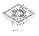
- a circuit pattern 2 serving as an island portion on which a semiconductor integrated circuit chip is to be mounted is formed on the surface of an Af N substrate 1.
- a plurality cf circuit patterns 4 each having a land portion 3 at its end are formed on the substrate 1.
- a plurality cf viafills (not shown) consisting of, e.g., tungsten are buried in holes formed in the substrate 1. The viafills are connected to the land portions 3, respectively, formed on the surface of the substrate 1.
- a plurality of lead bonding regions, e.g., pin bonding regions (not shown) are formed on the lower surface of the substrate 1. The pin bonding regions are connected to the viafills respectively.
- a frame-like pattern 5 for bonding a seal frame is formed on the periphery of the surface of the substrate 1.
- the Af N substrate 1 preferably has an oxygen con tent with an atomic ratio of 0.001 to 10 and a thermal conductivity of 130 to 280 W/m.K. That is, if the atomic ratio of oxygen content in the substrate is less than 0.001, it is difficult to satisfactorily increase a bonding strength with respect to an undercoating layer. If the oxygen content is more than 10 atm%, the thermal conductivity of the AfN substrate is decreased to be equal to that of alumina, thereby degrading an advantage of high thermal conductivity.
- the circuit pattern and the circuit patterns 4 each having the land portion 3 at its end are constituted to have multilayered structures to be described in the following items (i) and (ii).
- the metal oxynitride layer is used to increase a bonding strength of the bonding layer with respect to the AlN substrate and to prevent the bonding layer from being peeled from the metal oxynitride layer during a thermal cycle. More specifically, Af as a component of the metal oxynitride layer has an effect of increasing the bonding strength of the bonding layerwith respect to the Af N substrate. M1 as a high reactivity with Af, oxygen, and nitrogen and therefore has an effect of increasing the bonding strength of the bonding layer with respect to the Af N substrate. M2 has a high reactivity with Af, M1, oxygen, and nitrogen as other components of the metal oxynitride layer and also has a high reactivity with the component of the barrier layer.
- M2 has an effect of further increasing the bonding strength of the bonding layer with respect to the AlN substrate.
- O and N as other components of the metal oxynitride layer have an effect of matching lattice constants between the Af N substrate and the bonding layer and an effect of relaxing a thermal expansion difference therebetween.
- a ratio (atm%) of each component of the metal oxynitride layer is limited for the following reason.
- the thickness of the metal oxynitride layer is preferably 3 nm or more for the following reason. That is, if the thickness of the metal oxynitride layer is less than 3 nm, it is difficult to stably increase the bonding strength between the AlN substrate and the bonding layer.
- the upper limit of the thickness of the metal oxynitride layer is preferably 500 nm, for the purpose of suppressing the side-etching during the patterning of the metal oxynitride layer, and also rendering the circuit board thinner. More preferably, the thickness of the metal oxynitride layer is 10 to 350 nm.
- the bonding layer is used to increase a bonding strength of the barrier layer with respect to the metal oxynitride layer.
- the bonding layer most preferably consists of Ti.
- the thickness of the bonding layer is preferably 5 to 900 nm for the following reason. That is, if the thickness of the bonding layer is less than 5 nm, the metal of the layer cannot reacts adequately with the metal oxynitride, and the bonding strength with respect to the metal oxynitride layer is inevitably insufficient. If the thickness of the bonding layer exceeds 900 nm, since an internal stress of the bonding layer is increased, the bonding layer is easily peeled from the metal oxynitride layer. More preferably, the thickness of the bonding layer is 10 to 500 nm.
- the barrier layer has an effect of preventing mutual diffusion between the bonding layer and the Au conductor layer which are vertically stacked.
- the barrier layer most preferably consists of Ni.
- the thickness of the barrier layer is preferably 10 nm to 1 ⁇ m, and more preferably, 50 to 700 nm for the following reason. If the thickness of the barrier layer is less than 10 nm, it is difficult to satisfactorily achieve its barrier effect. If the thickness of the barrier layer is more than 1 ⁇ m, since an internal stress of the barrier layer is increased, the barrier layer is peeled from the bonding layer, or it is difficult to form a highly reliable circuit pattern since a side-etching degree is increased upon etching performed during patterning. More preferably, the thickness of the barrier layer is 30 to 700 nm.
- the thickness of the conductor layer is preferably 100 nm to 20 ⁇ m in consideration of a conductivity of the circuit pattern.
- the undercoating layer is used to increase a bonding strength of the main layer with respect to the AfN substrate and to prevent the main layer from being peeled from the undercoating layer during a thermal cycle. More specif ically, Af as a component of the undercoating layer has an effect of increasing the bonding strength of the main layer with respect to the Af N substrate. M1 has a high reactivity with Af, oxygen, and nitrogen and therefore has an effect of increasing the bonding strength of the main layer with respect to the Af N substrate. M2 has a high reactivity with Af, M1, oxygen, and nitrogen as other components of the undercoating layer and therefore has an effect of further increasing the bonding strength of the main layer with respect to the Af N substrate.
- Au has an effect of forming a compound with metals represented by M1 and M2 to further increase the bonding strength of the main layer with respect to the Af N substrate.
- O and N as other components of the undercoating layer have an effect of matching lattice constants between the AlN substrate and the main layer and an effect of relaxing a thermal expansion difference therebetween. ratio (atm%) of each component of the undercoating layer is limited for the following reason.
- the thickness of the undercoating layer is preferably 3 nm or more for the following reason. That is, if the thickness of the undercoating layer is less than 3 nm, it is difficult to stably increase the bonding strength between the AlN substrate and the main layer.
- the upper limit of the thickness of the undercoating layer is preferably 500 nm, for the purpose of suppressing the side-etching during the patterning of the undercoating layer, and also rendering the circuit board thinner. More preferably, the thickness of the undercoating layer is 8 to 500 nm.
- the main layer is used as a conductor portion of the circuit pattern. More specifically, M1 and M2 as a component of the main layer have an effect of increasing a bonding strength with respect to the undercoating layer. Au has an effect of decreasing a resistance of the main layer. O has an effect of further increasing the bonding strength with respect to the undercoating layer. A ratio (atm%) of each component of the main layer is limited for the following reason.
- the thickness of the main layer is preferably 300 nm to 10 ⁇ m. This is because, if the main layer is less than 300 nm thick, it can hardly have a uniform bonding strength with respect firmly to the undercoating layer. Conversely, if the main layer is more than 10 ⁇ m, the etching efficiency, which it must have during the etching, will decrease, making it difficult to form a fine circuit pattern.
- circuit pattern having the multilayered structure described in item (ii) above can also be formed by heating the circuit pattern having the structure described in item (i) above at 600°C to 1000°C.
- pin bonding regions and the frame-like pattern described above have a multilayered structure similar to those described in items (i) and (ii).
- a method of manufacturing a circuit pattern according to the present invention will be described in detail below by taking a circuit board on which a circuit pattern having the multilayered structure described in item (i) above is formed as an example.
- An alkali earth metal compound and/or rare earth element compound and a binder are added to an Af N powder to prepare a starting material, and the starting material is molded by a doctor blade method or the like to form an Af N green sheet.
- the alkali earth metal compound are an oxide, a carbide, a fluoride, a carbonate, an oxalate, a nitrate, and an alkoxide of Ca, Ba, and Sr.
- Examples of the rare earth element compound are an oxide, a carbide, a fluoride, a carbonate, an oxalate, a nitrate, and an alkoxide of Y, La, Ce, Nd, Dy, and Pr.
- compounds of Y, La, and Ce can be suitably used.
- holes are formed in the green sheet by using, e.g., a drill, and a tungsten paste is filled in the holes.
- degreasing and calcining are performed to form an Af N substrate in which the tungsten viafills are filled in the holes.
- the surface of the Af N substrate is polished to adjust a surface roughness to be suitable for forming a metal oxynitride layer.
- a metal oxynitride layer consisting ofAf, M1, M2, O, and N is formed on the substrate by a general film formation technique such as a vacuum deposition method, a sputter-deposition method a cluster ion beam method, an ion plating or an ion implantation method.
- a substrate temperature, an atmosphere, a vacuum degree, and a film formation rate are adjusted as needed.
- the substrate surface is preferably cleaned well by a wet cleaning method, a reverse sputtering method, or the like. Since, however, the Af N substrate is unstable with respect to a strong acid and a strong alkali, a cleaning fluid must be carefully selected.
- a neutral cleaning fluid is preferably used.
- a bonding layer consisting of a metal represented by M1 a barrier layer consisting of a metal represented by M2, and a conductor layer consisting of Au are sequentially formed.
- the conductor layer may be formed on the barrier layer by wet plating.
- a resist pattern is formed on the conductor layer by photolithography, and the above four layers are sequentially etched and patterned by using the formed pattern as a mask.
- the conductor layer made of Au is etched with, for example, an etchant which is a mixture of KI, 12, and deionized water.
- the layer is etched with, for ex ample, an etchant which is a mixture of C U S0 4 , HCf, ethyl alcohol, and deionized water, if the barrier layer is made of Ni. It is etched by means of, for example, ion milling if the barrier layer is made of Pt. It is etched with, for example, an etchant comprising aqua regia and acetic acid if the barrier layer is made of Pd.
- the bonding layer and the metal oxynitride layer are etched with, for example, an etchant which is a mixture of HF and deionized water.
- the circuit pattern can be formed by causing parts of the bonding layer and the barrier layer to intermix with the metal oxynitride layer as the bonding layer and the barrier layer grow gradually. In this case, it does not matter if intermixing occurs between the bonding layer and the barrier layer, or if a gradient structure is formed between these layers. Further, up to 50 wt% of the M2 component may diffuse into the bonding layer.
- the upper most layer can be wet-plated with Au, or wet-plated first with Ni and then with Au.
- the conductor layer can be made of Cu, and a thin Au layer can be formed on the conductor layer.
- the bonding layer, the barrier layer, and the conductor layer are formed in the order named, but also a thin film resistor and a thin film capacitor may be additionally formed.
- a circuit pattern 2 serving as an island portion on which a semiconductor integrated circuit chip is to be mounted is formed on the surface of an AlN substrate 1.
- a plurality of circuit patterns 4 each having a land portion 3 at its end are formed on the substrate 1.
- a plurality of via fills (not shown) consisting of, e.g., tungsten are buried in holes formed in the substrate 1. The viafills are connected to the land portions respectively, formed on the surface of the substrate 1.
- a plurality of lead bonding regions, e.g., pin bonding regions (not shown) are formed on the lower surface of the substrate 1. The pin bonding regions are connected to the viafills, respectively.
- Aframe-like pattern 5 for bonding a seal frame is formed on the periphery of the surface of the substrate 1.
- a brazing material layers (not shown) are bonded on the pin bonding regions, respectively. Leads, e.g., pins 6 are bonded to the brazing material layers respectively.
- a frame-like brazing material layer 7 is bonded to the frame-like pattern 5.
- a seal frame 8 is bonded to the brazing material layer 7.
- the circuit pattern 2 and the circuit patterns 4 each having the land portion 3 at its end are constituted to have, e.g., the multilayered structure described in item (i) or (ii) above.
- the pin bonding regions and the frame-like pattern 5, and the brazing material layers have the following arrangement.
- the pin bonding regions and the frame-like pattern have a multilayered structure in which an undercoating layer represented by formula Al u M1 v M2 w Cu x O y N z (wherein M1 represents a metal selected from the group consisting of Ti, Cr, Ta, and Zr, M2 represents a metal selected from the group consisting of Ni, Pt, Pd, W, Nb, and Mo, u represents 0.1 to 25 atm%, v represents 0.2 to 35 atm%, w represents 0.1 to 50 atm%, x represents 0.005 to 1.5 atm%, y represents 0 to 1.5 atm%, and z represents 0.5 to 40 atm%) and a main layer represented by formula M1 x M2 y Cu z (wherein M1 represents a metal selected from the group consisting of Ti, Cr, Ta, and Zr, M2 represents a metal selected from the group consisting of Ni, Pt, Pd, W, Nb, and Mo, x represents 1 to 50 atm%
- the undercoating layer is used to increase a bonding strength of the main layer with respect to the Af N substrate.
- the undercoating layer is also used to prevent the main layer from being peeled from the undercoating layer during a thermal cycle.
- the undercoating layer is used to relax a thermal expansion difference between the Af N substrate and the pins or the seal frame. More specifically, Af as a component of the undercoating layer has an effect of increasing the bonding strength of the main layer with respect to the AlN substrate.
- M1 and M2 have an effect of increasing the bonding strength of the main layer with respect to the Af N substrate and also have an effect of relaxing the thermal expansion difference between the Af N substrate and the pins or the seal frame.
- Cu has an effect of forming a compound with metals represented by M1 and M2 to further increase the bonding strength of the main layer with respect to the Af N substrate.
- O and N as other components of the undercoating layer have an effect of relaxing the thermal expansion difference between the Af N substrate and the pins or the seal frame.
- the ratio (atm%) of each component of the undercoating layer is limited for the following reasons.
- the thickness of the undercoating layer is preferably 3 nm or more for the following reason. That is, if the thickness of the undercoating layer is less than 3 nm, it is difficult to stably increase the bonding strength with respect to the Af N substrate and the main layer.
- the upper limit of the thickness of the undercoating layer is preferably 500 nm, for the purpose of suppressing the side-etching during the patterning of the undercoating layer, and also rendering the circuit board thinner. More preferably, the thickness of the undercoating layer is 5 to 500 nm.
- the main layer is used to increase a bonding strength of the brazing material layer with respect to the undercoating layer. More specifically, M1 as a compo-nent of the main layer has an effect of suppressing a thermal expansion difference with respect to the pins or the seal frame to increase a bonding strength of the pins or the seal frame. M2 and Cu have an effect of increasing a bonding strength of the bonding layer with respect to the undercoating layer.
- the ratio (atm%) of each component of the main layer is limited for the following reason.
- the thickness of the main layer is preferably 10 to 500 nm. This is because, if the main layer is less than 10 nm thick, it can hardly be bonded firmly to the under coating layer, though the difference in thermal expansion between it and the pins or the seal frame. Conversely, if the main layer is more than 500 nm thick, its bonding strength with respect to the pins or the seal frame will decrease during the heat cycle.
- the brazing material layer consists of a composition bonded to the main layer of the pin bonding regions or the flame-like pattern and represented by formula Ag x CuyAu, (wherein x represents 5 to 90 atm%, y represents 1 to 50 atm%, and represents 1 to 50 atm%).
- the brazing material layer is used to increase a bonding strength of the pins or the seal frame with respect to the main layer.
- the ratio (atm%) of each component of the brazing material layer is limited for the following reason.
- the thickness of the brazing material layer is preferably 1 to 100 ⁇ m. This is because, if the brazing material layer is less than 1 ⁇ m thick, its bonding strength with respect to the pins or the seal frame will likely decrease. Conversely, if the brazing material layer is more than 100 ⁇ m thick, the Af N substrate will have micro-cracks due to the difference in thermal expansion between the brazing material layer and the AlN substrate, possibly impairing the strength of the bonding between the Af N substrate on the one hand, and the pins or the seal frame on the other hand.
- pin bonding regions and the frame-like pattern having the arrangement as described in item (a) above and the brazing material layer having the arrangement as described in item (b) above can also be formed by the following process. This process will be described below by taking the pin bonding regions as an example. That is, pin bonding regions having the multilayered structure as described in item (i) or (ii) above are formed, an Ag-Cu-based brazing material layer is arranged at the pin bonding regions, and pins are arranged on the brazing mate-rial layer and bonded thereto by heating at a temperature of 780°C to 1000°C.
- the layers of the multilayered structure of item (i) or (ii) and the Ag-Cu-based brazing material layer are mutually diffused to form the pin bonding regions having the arrangement described in item (a) above and the brazing material layer having the arrangement described in item (b) above.
- the pins 6 and the seal frame 8 may consist of, e.g., an Ni-Fe-Cu alloy-based-Kovar or a 42% Ni-Fe alloy.
- a circuit board according to the present invention has a circuit pattern having a multilayered structure in which a metal oxynitride layer represented by formula Al u M1 v M2 x O y N z (wherein M1 represents a metal selected from the group consisting of Ti, Or, Ta, and Zr, M2 represents a metal selected from the group consisting of Ni, Pt, Pd, W, Nb, and Mo, u represents 3 to 50 atm%, v represents 3 to 78 atm%, x represents 0 to 50 atm%, y represents 0.005 to 25 atm%, and z represents 5 to 70 atm%), a bonding layer consisting of a metal represented by M1, a barrier layer consisting of a metal represented by M2, and a conductor layer consisting of Au are stacked in the order named.
- a metal oxynitride layer represented by formula Al u M1 v M2 x O y N z
- the Af N substrate since the Af N substrate has a high thermal conductivity, it can efficiently radiate heat generated by an active element mounted on the circuit pattern, e.g., an IC chip or an LSI chip.
- a circuit pattern having a high bonding strength with respect to the Af N substrate and free from peeling or disconnection during a thermal cycle can be formed.
- formation of a circuit pattern having a high bonding strength with respect to an Af N substrate generally depends on lattice constants of the circuit pattern and the AlN substrate, a difference between thermal expansion coefficients, and the presence/absence of chemical reactivity.
- the metal oxynitride layer represented by the above formula contains Af, M1, O, and N as its components at predetermined atomic ratios, it can increase the bonding properties of the bonding layer with respect to the Af N substrate and can prevent the bonding layer from being peeled from the metal oxynitride layer.
- the bonding strength of the bonding layer with respect to the Af N substrate can be further increased.
- the bonding layer can increase the bonding strength of the barrier layer with respect to the metal oxynitride layer.
- the barrier layer has an effect of preventing mutual diffusion of the bonding layer and the Au conductor layer which respectively underlies and overlies the barrier layer.
- the conductor layer serves as a conductor portion for decreasing a resistance of the circuit pattern. Therefore, a good circuit pattern which has a high bonding strength with respect to the Af N substrate and in which peeling and disconnection of each layer during a thermal cycle can be prevented can be formed.
- the circuit board as described above has a circuit pattern having high heat radiation properties and a high bonding strength with respect to the AlN substrate and therefore can be effectively used as a semiconductor package or a semiconductor module which can mount active elements such as IC chips or LSI chips at a high packing density.
- Another circuit board according to the present invention has a circuit board having a multilayered structure in which an undercoating layer represented by formula Al u M1 v M2 w Au x O y N z (wherein M1 is a metal selected from the group consisting of Ti, Cr, Ta, and Zr, M2 represents a metal selected from the group consisting of Ni, Pt, Pd, W, Nb, and Mo, u represents 0.1 to 40 atm%, v represents 0.5 to 50 atm%, w represents 0.1 to 50 atm%, x represents 0.05 to 30 atm%, y represents 0 to 20 atm%, and z represents 0.1 to 40 atm%) and a main layer represented by formula M1 w M2 x Au y O z (wherein M1 represents a metal selected from the group consisting of Ti, Cr, Ta, and Zr, M2 represents a metal selected from the group consisting of Ni, Pt, Pd, W, Nb, and Mo, w represents 0.5 to 50
- the Af N substrate since the Af N substrate has a high thermal conductivity, it can efficiently radiate heat generated by an active element mounted on the circuit pattern such as an IC ship or an LSI chip.
- a good circuit pattern having a high bonding-strength with respect to the Af N substrate and free from peeling or disconnection during a thermal cycle can be formed.
- the undercoating layer represented by the above formula contains Al, M1, M2, and N as its components at predetermined atomic ratios, it can increase the bonding properties of the main layer with respect to the Af N substrate and can prevent the main layer from being peeled from the undercoating layer during a thermal cycle.
- the undercoating layer contains especially O at a predetermined atomic ratio, matching of lattice constants and relaxation of a thermal expansion difference between the AlN substrate and the main layerwhich respectively underlies and overlies the undercoating layer can be further improved.
- the main layer represented by the above formula contains M1, M2, and Au as its components at predetermined atomic ratios, it can increase its bonding strength with respect to the undercoating layer and has a low resistance.
- the main layer contains especially O at a predetermined atomic ratio, the bonding strength with respect to the undercoating layer can be further increased. Therefore, a circuit pattern which has a high bonding strength with respect to the Af N substrate and in which each layer can be prevented from being peeled or disconnected during a thermal cycle can be formed.
- the above circuit board has a circuit pattern having good heat radiation properties and a high bonding strength with respect to the AlN substrate and therefore can be effectively used as a semiconductor package or a semiconductor module which can mount active elements such as IC chips or LSI chips at a high density.
- Still another circuit board comprises pin bonding regions having a multilayered structure in which an undercoating layer represented by formula Al u M1 v M2 w Cu x O y N z (wherein M1 represents a metal selected from the group consisting of Ti, Cr, Ta, and Zr, M2 represents a metal selected from the group consisting of Ni, Pt, Pd, W, Nb, and Mo, u represents 0.1 to 25 atm%, v 0.2 to 35 atm%, w represents 0.1 to 50 atm%, x represents 0.005 to 1.5 atm%, y represents 0 to 1.5 atm%, and z represents 0.5 to 40 atm%) and a main layer represented by formula M1 x M2 y Cu z (wherein M1 represents a metal selected from the group consisting of Ti, Cr, Ta, and Zr, M2 represents a metal selected from the group consisting of Ni, Pt, Pd, W, Nb, and Mo, x represents 1 to 50 atm%,
- the Af N substrate has a radiate heat generated by an active element mounted on the circuit pattern such as an IC chip or an LSI chip.
- the pins can be bonded to the AlN substrate with a high bonding strength, and peeling of the pins during a thermal cycle can be prevented.
- the undercoating layer which is a lower layer constituting the pin bonding regions and represented by the above formula contains Af, M1, M2, Cu, and N as its components at predetermined atomic ratios, it can increase the bonding properties of the main layer with respect to the AlN substrate.
- the undercoating layer can prevent the main layer from being peeled from the undercoating layer in a thermal cycle.
- a thermal expansion difference between the AlN substrate and the pins can be relaxed.
- the undercoating layer contains especially O at a predetermined atomic ratio, the thermal expansion difference between the AlN substrate and the pins can be further relaxed.
- the main layer which is an upper layer constituting the pin bonding regions and represented by the above formula contains M1, M2, and Cu as its components at predetermined atomic ratios, it can increase the bonding strength of the brazing material layer with respect to the undercoating layer.
- the brazing material layer represented by the above formula contains Ag, Cu, and Au as its components at predetermined atomic ratios, it can increase the bonding strength of the pins with respect to the AlN substrate and can prevent peeling of the pins during a thermal cycle.
- the above circuit board has good heat radiation properties and a high bonding strength with respect to the AlN substrate and therefore can be effectively used as a semiconductor package or a semiconductor module which can mount active elements such as IC chips or LSI chips at a high density.
- This circuit board has the pins and the seal frame having good heat radiation properties and a high bonding strength with respect to the Af N substrate and therefore can be effectively used as a semiconductor package or a semiconductor module which can mount active elements such as IC chips or LSI chips at a high packing density and can air-tightly seal the mounted active elements.
- Lapping and polishing were performed such that an average linear surface roughness of the AlN substrate was 150 nm, and wet cleaning and reverse sputtering were performed on the substrate surface.
- 100-nm thick metal oxynitride layers were formed on the two surfaces of the substrate under the conditions listed in Table 1 to be presented later by using a sputter-deposition apparatus. Subsequently, without breaking the vacuum of the sputter-deposition apparatus, a 50-nm thick Ti bonding layer, a 500-nm thick barrier layer, and a 1- ⁇ m thick Au conductor layer were sequentially formed on the metal oxynitride layer. Note that Ni was used as the barrier layer in Examples 1, 4, and 5, Pt was used as the barrier layer in Example 2, and Pd was used as the barrier layer in Example 3.
- a resist pattern was formed by photolithography on the conductor layer formed on the upper surface side of the substrate, and the conductor layer, the barrier layer, the bonding layer, and the metal oxynitride layer were sequentially selectively removed by etching by using the resist pattern as a mask, thereby forming a circuit pattern, a circuit pattern having a land portion at its end, and a frame-like pattern.
- etching was similarly performed to form pin bonding regions.
- circuit boards having the arrangement shown in Fig. 1 were manufactured following the same procedures as in Example 1 except that a metal oxynitride layer was formed under the conditions listed in Table 1 to be presented later on the surface of an Af N substrate having a thermal conductivity and subjected to a surface treatment as described in Example 1.
- a bonding strength of a circuit pattern and its state obtained after a TCT were checked for each circuit board of Examples 1 to 5 and Comparative Examples 1 and 2. The results are summarized in Table 1. Note that the bonding strength and the characteristics (strength characteristics and peeling characteristics) after the TCT were evaluated by the following method.
- An Sn-plated copper wire having a diameter of 0.7 mm was bonded on a circuit pattern by using an Sn-Pb-based solder. Subsequently, the copper wire was stretched at a rate of 5 cm/min. by using a tensile strength tester (#4301 available from Instron Co.), thereby evaluating the bonding strength of the circuit pattern.
- the circuit board was cooled to -50°C, it was heated up to 150°C and held at this temperature for 30 minutes, and this temperature cycle was repeatedly performed 1,000 times. Thereafter, the bonding strength of a circuit pattern of this circuit board was measured following the same procedures as in item (i) above. In this case, if the bonding strength as obtained before the TCT was obtained, “strength not decreased” was determined. If the bonding strength was decreased as compared with that obtained before the TCT, "strength decreased” was determined.
- Amending tape (scotch 810 available from 3M Co.) was adhered on a circuit pattern of a circuit board subjected to the TCT, and a peeling test was conducted by pulling the tape with a sufficient strength. Thereafter, the adhesion surface of the tape and the surface of the circuit pattern were observed by an electron microscope. A this time, if a peeled piece of the circuit pattern was adhered on the tape surface or a peeled mark was formed on the circuit pattern, "peeled” was evaluated. If no peeled piece nor mark was found, "not peeled” was evaluated.
- each of the circuit patterns of Examples 1 to 5 having a metal oxynitride layer represented by formula Al u Ti v O y N z (wherein u represents 3 to 50 atm%, v represents 3 to 78 atm%, y represents 0.005 to 25 atm%, and z represents 5 to 70 atm%) has a high bonding strength with respect to the Af N substrate and causes no decrease in bonding strength nor peeling in the evaluation performed after 1,000 cycles of the TCT, i.e., has good bonding properties.
- the circuit pattern of Comparative Example 1 having 0 atm% of an O amount as a component of the metal oxynitride layer has a low bonding strength with respect to the Af N substrate and causes peeling of the circuit pattern in the evaluation performed after 1,000 cycles of the TCT.
- the circuit pattern of Comparative Example 2 having less than 3 atm% of a Ti amount as a component of the metal oxynitride layer has a low bonding strength with respect to the Af N substrate and causes peeling of the circuit pattern in the evaluation performed after 1,000 cycles of the TCT.
- circuit boards of Examples 1 to 5 were subjected to a heat-resistance test, wherein they were left to stand at 500°C for 5 minutes. They were also subjected to PCT test, wherein they were left to stand at 121°C under 2 atm for 2,000 hours. The circuit boards, thus tested, were found to have their circuit patterns intact.
- Example 2 Thereafter, following the same procedures as in Example 1, the layers formed on the upper surface side of the substrate were selectively etched to form a circuit pattern, a circuit pattern having a land portion at its end, and a frame-like pattern. In addition, following the same procedures as in Example 1, the layers formed on the lower surface side of the substrate were selectively etched to form pin bonding regions. By performing these manufacturing steps, four types of circuit boards having the structure shown in Fig. 1 were manufactured.
- Example 2 Thereafter, following the same procedures as in Example 1, the layers formed on the upper surface side of the substrate were selectively etched to form a circuit pattern, a circuit pattern having a land portion at its end, and a frame-like pattern. In addition, following the same procedures as in Example 1, the layers formed on the lower surface side of the substrate were selectively etched to form pin bonding regions. By performing these manufacturing steps, two types of circuit boards having the structure shown in Fig. 1 were manufactured.
- Example 2 Thereafter, following the same procedures as in Example 1, the layers formed on the upper surface side of the substrate were selectively etched to form a circuit pattern, a circuit pattern having a land portion at its end, and a frame-like pattern. In addition, following the same procedures as in Example 1, the layers formed on the lower surface side of the substrate were selectively etched to form pin bonding regions. By performing these manufacturing steps, three types of circuit boards having the structure shown in Fig. 1 were manufactured.
- each of the circuit patterns of Examples 6 to 11 having a metal oxynitride layer represented by formula Al u Ti v Ni x O y N z (wherein u represents 3 to 50 atm%, v represents 3 to 78 atm%, x represents 0.0001 to 50 atm%, y represents 0.005 to 25 atm%, and z represents 5 to 70 atm%) has a high bonding strength with respect to the Af N substrate and causes no decrease in bonding strength nor peeling in the evaluation performed after 1,000 cycles of the TCT, i.e., has good bonding properties.
- the circuit pattern of Comparative Example 3 having 0 atm% of an Af amount as a component of the metal oxynitride layer has a low bonding strength with respect to the Af N substrate and causes peeling of the circuit pattern in the evaluation performed after 1,000 cycles of the TCT.
- the circuit pattern of Comparative Example 4 having less than 3 atm% of a Ti amount as a component of the metal oxynitride layer has a low bonding strength with respect to the Af N substrate and causes peeling of the circuit pattern in the evaluation performed after 1,000 cycles of the TCT.
- circuit pattern of Comparative Example 5 having 0 atm% of an N amount as a component of the metal oxynitride layer has a low bonding strength with respect to the Af N substrate and causes peeling of the circuit pattern in the evaluation performed after 1,000 cycles of the TCT.
- circuit boards of Examples 6 to 11 were subjected to a heat-resistance test, wherein they were left to stand at 500°C for 5 minutes. They were also subjected to PCT test, wherein they were left to stand at 121°C under 2 atm for 2,000 hours. The circuit boards, thus tested, were found to have their circuit patterns intact.
- Example 2 Thereafter, following the same procedures as in Example 1, the layers formed on the upper surface side of the substrate were selectively etched to form a circuit pattern, a circuit pattern having a land portion at its end, and a frame-like pattern. In addition, following the same procedures as in Example 1, the layers formed on the lower surface side of the substrate were selectively etched to form pin bonding regions. By performing these manufacturing steps, two types of circuit boards having the structure shown in Fig. 1 here manufactured.
- Example 2 Thereafter, following the same procedures as in Example 1, the layers formed on the upper surface side of the substrate were selectively etched to form a circuit pattern, a circuit pattern having a land portion at its end, and a frame-like pattern. In addition, following the same procedures as in Example 1, the layers formed on the lower surface side of the substrate were selectively etched to form pin bonding regions. By performing these manufacturing steps, two types of circuit boards having the structure shown in Fig. 1 were manufactured.
- each of the circuit patterns of Examples 12 and 13 having a metal oxynitride layer represented by formula Al u Ti v W x O y N z (wherein u represents 3 to 50 atm%, v represents 3 to 78 atm%, x represents 0.0001 to 50 atm%, y represents 0.005 to 25 atm%, and z represents 5 to 70 atm%) has a high bonding strength with respect to the Af N substrate and causes no decrease in bonding strength nor peeling in the evaluation performed after 1,000 cycles of the TCT, i.e., has good bonding properties.
- the circuit pattern of Comparative Example 6 having more than 70 atm% of an N amount as a component of the metal oxynitride layer has a low bonding strength with respect to the Af N substrate and causes peeling of the circuit pattern in the evaluation performed after 1,000 cycles of the TCT.
- the circuit pattern of Comparative Example 7 having more than 25 atm% of an O amount as a component of the metal oxynitride layer has a low bonding strength with respect to the Af N substrate and causes peeling of the circuit pattern in the evaluation performed after 1,000 cycles of the TCT.
- circuit boards of Examples 12- and 13 were subjected to a heat-resistance test, wherein they were left to stand at 500°C for 5 minutes. They were also subjected to PCT test, wherein they were left to stand at 121°C under 2 atm for 2,000 hours. The circuit boards, thus tested, were found to have their circuit patterns intact.
- Example 2 Thereafter, following the same procedures as in Example 1, the layers formed on the upper surface side of the substrate were selectively etched to form a circuit pattern, a circuit pattern having a land portion at its end, and a frame-like pattern. In addition, following the same procedures as in Example 1, the layers formed on the lower surface side of the substrate were selectively etched to form pin bonding regions. By performing these manufacturing steps, four types of circuit boards having the structure shown in Fig. 1 were manufactured.
- Example 2 Thereafter, following the same procedures as in Example 1, the layers formed on the upper surface side of the substrate were selectively etched to form a circuit pattern, a circuit pattern having a land portion at its end, and a frame-like pattern. In addition, following the same procedures as in Example 1, the layers formed on the lower surface side of the substrate were selectively etched to form pin bonding regions. By performing these manufacturing steps, four types of circuit boards having the structure shown in Fig. 1 were manufactured.
- each of the circuit patterns of Examples 14 to 21 having a metal oxynitride layer represented by formula Al u M1 v M2 x O y N z (wherein M1 represents a metal selected from the group consisting of Ti, Cr, Zr, and Ta, M2 represents a metal selected from the group consisting of Mo, Ni, Nb, and W, u represents 3 to 50 atm%, v represents 3 to 78 atm%, x represents 0.0001 to 50 atm%, y represents 0.005 to 25 atm%, and z represents 5 to 70 atm%) has a high bonding strength with respect to the Af N substrate and causes no decrease in bonding strength nor peeling in the evaluation performed after 1,000 cycles of the TCT, i.e., has good bonding properties.
- M1 represents a metal selected from the group consisting of Ti, Cr, Zr, and Ta
- M2 represents a metal selected from the group consisting of Mo, Ni, Nb, and W
- u represents 3 to 50 atm%
- circuit boards of Examples 14 to 21 were subjected to a heat-resistance test, wherein they were left to stand at 500°C for 5 minutes. They were also subjected to PCT test, wherein they were left to stand at 121 °C under 2 atm for 2,000 hours. The circuit boards, thus tested, were found to have their circuit patterns intact.
- the main and undercoating layers were sequentially selectively removed by etching by using the resist pattern as a mask, thereby forming a circuit pattern, a circuit pattern having a land portion at its end, and a frame-like pattern.
- selective etching was similarly performed to form pin bonding regions.
- Example 7 Following the same procedures as in Example 1, a bonding strength of a circuit board and its characteristics (strength characteristics and peeling characteristics) obtained after 1,000 cycles of the TCT were checked for each of the circuit boards of Examples 22 and 23. In addition, the presence/absence of peeling of each circuit pattern before the TCT was performed was checked by a peeling test according to the method of item (iii) in Example 1. The results are listed in Table 7.
- the layers formed on the upper surface side of the substrate were selectively removed by etching to form a circuit pattern, a circuit pattern having a land portion at its end, and a frame-like pattern.
- the layers formed on the lower surface side of the substrate were selectively etched to form pin bonding regions.
- Example 8 Following the same procedures as in Example 1, a bonding strength of a circuit board and its characteristics (strength characteristics and peeling characteristics) obtained after 1,000 cycles of the TCT were checked for each of the circuit boards of Examples 24 and 25. In addition, the presence/absence of peeling of each circuit pattern before the TCT was performed was checked by a peeling test according to the method of item (iii) in Example 1. The results are listed in Table 8.
- the layers formed on the upper surface side of the substrate were selectively removed by etching to form a circuit pattern, a circuit pattern having a land portion at its end, and a frame-like pattern.
- the layers formed on the lower surface side of the substrate were selectively etched to form pin bonding regions.
- Example 1 Following the same procedures as in Example 1, a bonding strength of a circuit board and its characteristics (strength characteristics and peeling characteristics) obtained after 1,000 cycles of the TCT were checked for each of the circuit boards of Examples 26 and 27. In addition, the presence/absence of peeling of each circuit pattern before the TCT was performed was checked by a peeling test according to the method of item (iii) in Example 1. The results are listed in Table 9.
- each of the circuit patterns of Examples 22 to 27 having an undercoating layer represented by formula Al u M1 v M2 w Au x O y N z (wherein M1 represents a metal selected from the group consisting of Ti, Cr, Ta, and Zr, M2 represents a metal selected from the group consisting of Ni, W, Nb, and Mo, u represents 0.1 to 40 atm%, v represents 0.5 to 50 atm%, w represents 0.1 to 50 atm%, x represents 0.05 to 30 atm%, y represents 0 to 20 atm%, and z represents 0.1 to 40 atm%) and a main layer represented by formula MlwM2xAuYO, (wherein M1 represents a metal selected from the group consisting of Ti, Cr, Ta, and Zr, M2 represents a metal selected from the group consisting of Ni, W, Nb, and Mo, w represents 0.5 to 50 atm%, x represents 0.1 to-50 atm
- the layers formed on the upper surface side of the substrate were selectively removed by etching to form a circuit pattern, a circuit pattern having a land portion at its end, and a frame-like pattern.
- the layers formed on the lower surface side of the substrate were selectively etched to form pin bonding regions.
- an Ag-Cu-based brazing material layer was bonded to the headers of pins made of Kovar consisting of 53.48 wt% of Fe, 29 wt% of Ni, 17 wt% of Co, 0.2 wt% of Si, 0.3 wt% of Mn, and 0.02 wt% of C. Note thatthe diameter of the pin portion of each pin was 0.3 mm, and the diameter of the header was 0.6 mm.
- an Ag-Cu-based brazing material layer was bonded to the lower surface of a Kovar seal frame.
- the brazing material layer of each of the pins was temporarily fixed on a pin bonding region by using a jig, and the brazing material layer of the seal frame was temporarily fixed on the frame-like pattern by using a jig.
- Each of the circuit boards of Examples 28 and 29 had the constitution of the pin bonding region and the brazing material layer formed thereon, and the circuit pattern, which were as is shown in Table 10 and obtained due to an effect of the heat treatment performed in the bonding step.
- a bonding strength of a circuit pattern obtained before the pin bonding step was checked for each circuit board in accordance with the method of item (i) in Example 1.
- a pin tensile strength at the pin bonding region and characteristics (strength characteristics) obtained after the TCT at the region of each circuit board were checked.
- a bonding strength of the circuit pattern, the presence/absence of peeling obtained by a peeling test, and characteristics (strength characteristics and peeling characteristics) obtained afterthe TCT were checked for each circuit board.
- a pin at a pin bonding region was pulled at a rate of 5 cm/min. by using a tensile strength tester (#4301 available from Instron Co.) to measure the pin tensile strength.
- An Sn-plated copper wire having a diameter of 0.7 mm was bonded on a circuit pattern by using an Sn-Pb-based solder. Subsequently, the copper wire was pulled at a rate of 5 cm/min. by using a tensile strength tester (#4301 available from Instron Co.) to evaluate the bonding strength of the circuit pattern.
- circuit board After the circuit board was cooled to -50°C, it was heated up to 150°C and held at the temperature for 30 minutes, and this temperature cycle was repeatedly performed 1,000 times. Thereafter, a bonding strength of a circuit of the circuit board was measured following the same procedures as in item (2-1) above. In this case, if the same tensile strength as that obtained, before the TCT was obtained, "strength not decreased” was determined. If the bonding strength was decreased as compared with that obtained before the TCT, “strength decreased” was determined. If “strength decreased” was determined, the bonding strength was also listed.
- a mending tape (scotch 810 available from 3M Co.) was adhered on a circuit pattern of a circuit board subjected to the TCT, and a peeling test was conducted by pulling the tape with a sufficient strength. Thereafter, the adhesion surface of the tape and the surface of the circuit pattern were observed by using an electron microscope. In this case, if a peeled piece was adhered on the tape surface or a peeled mark was formed on the circuit pattern, "peeled” was evaluated. If no peeled piece nor mark was found, "not peeled” was evaluated.
- the layers formed on the upper surface side of the substrate were selectively removed by etching to form a circuit pattern, a circuit pattern having a land portion at its end, and a frame-like pattern.
- the layers formed on the lower surface side of the substrate were selectively etched to form pin bonding regions.
- an Ag-Cu-based brazing material layer was bonded to the headers of pins similar to those used in Example 28.
- an Ag-Cu-based brazing material layer was bonded to the lower surface of a Kovar seal frame.
- the brazing material layer of the each of the pins was temporarily fixed on a pin bonding region by using a jig, and the brazing material layer of the seal frame was temporarily fixed on the frame-like pattern by using a jig.
- Each of the circuit boards of Examples 30 and 31 had the constitution of the pin bonding region and the brazing material layer formed thereon, and the circuit pattern, which were as is shown in Table 11 and obtained due to an effect of the heat treatment performed in the bonding step.
- a bonding strength of a circuit board obtained before the pin bonding step a pin tensile strength of a pin bonding region, and characteristics (strength characteristics) obtained after the TCT were checked for each circuit board.
- a bonding strength of a circuit board of each circuit board, the presence/absence of peeling obtained by the peeling test, and characteristics (strength characteristics and peeling characteristics) obtained after the TCT were checked. The results are summarized in Table 11.
- Example 2 Following the same procedures as in Example 1, lapping, polishing, wet cleaning, and reverse sputtering were performed on the surface of an Af N substrate having an oxygen content of 0.03 at% and a thermal conductivity of 270 W/m.K and having viafills consisting of W.
- Metal oxynitride layers were formed on the two surfaces of the substrate under the conditions listed in Table 12 to be presented later by using a sputter-deposition apparatus. Subsequently, without breaking the vacuum in the sputter-deposition apparatus, a bonding layer, a barrier layer, and a conductor layer were sequentially formed on the metal oxynitride layer under the conditions listed in Table 12.
- the layers formed on the upper surface side of the substrate were selectively removed by etching to form a circuit pattern, a circuit pattern having a land portion at its end, and a frame-like pattern.
- the layers formed on the lower surface side of the substrate were selectively etched to form pin bonding regions.
- an Ag-Cu-based brazing material layer was bonded to the headers of pins similar to those that used in Example 28.
- an Ag-Cu-based brazing material layer was bonded to the lower surface of a Kovar seal frame.
- the brazing material layer of each of the pins was temporarily fixed on a pin bonding region by using a jig, and the brazing material layer of the seal frame was temporarily fixed on the frame-like pattern by using a jig.
- Each of the circuit boards of Comparative Examples 8 and 9 had the constitution of the pin bonding region and the brazing material layer formed thereon, and the circuit pattern, which were as is shown in Table 12 and obtained due to an effect of the heat treatment performed in the bonding step.
- a bonding strength of a circuit board obtained before the pin bonding step a pin tensile strength of a pin bonding region, and characteristics (strength characteristics) obtained after the TCT were checked for each circuit board.
- a bonding strength of a circuit board of each circuit board, the presence/absence of peeling obtained by the peeling test, and characteristics (strength characteristics and peeling characteristics) obtained after the TCT were checked. The results are summarized in Table 12.
- the layers formed on the upper surface side of the substrate were selectively removed by etching to form a circuit pattern, a circuit pattern having a land portion at its end, and a frame-like pattern.
- the layers formed on the lower surface side of the substrate were selectively etched to form pin bonding regions.
- an Ag-Cu-based brazing material layer was bonded to the headers of pins similar to those used in Example 28.
- an Ag-Cu-based brazing material layer was bonded to the lower surface of a Kovar seal frame.
- the brazing material layer of each of the pins was temporarily fixed on a pin bonding region by using a jig, and the brazing material layer of the seal frame was temporarily fixed on the frame-like pattern by using a jig.
- Each of the circuit boards of Comparative Examples 10 and 11 had the constitution of the pin bonding region and the brazing material layer formed thereon, and the circuit pattern, which were as is shown in Table 13 and obtained due to an effect of the heat treatment performed in the bonding step.
- a bonding strength of a circuit board obtained before the pin bonding step a pin tensile strength of a pin bonding region, and characteristics (strength characteristics) obtained after the TCT were checked for each circuit board.
- a bonding strength of a circuit board of each circuit board, the presence/absence of peeling obtained by the peeling test, and characteristics (strength characteristics and peeling characteristics) obtained after the TCT were checked. The results are summarized in Table 13.
- each of the circuit boards of Examples, 28 to 31 in which the pins are bonded at a predetermined temperature to the pin bonding regions having a metal oxynitride layer represented by formula Af u Ml v OyN z (wherein M1 represents a metal selected from the group consisting of Ti, Ta, and Cr, u represents 3 to 50 atm%, v represents 3 to 78 atm%, y represents 0.005 to 25 atm%, and z represents 5 to 70 atm%) has a high bonding strength of the pin with respect to the AfN substrate and causes no decrease in the bonding strength of the pin in the evaluation performed after 1,000 cycles of the TCT, i.e., has good characteristics.
- M1 represents a metal selected from the group consisting of Ti, Ta, and Cr
- u represents 3 to 50 atm%
- v represents 3 to 78 atm%
- y represents 0.005 to 25 atm%
- z represents 5 to 70 atm
- each of the circuit boards of Examples 28 to 31 obtained after the circuit pattern having the metal oxynitride layer is heated at the above temperature has a high bonding strength of the circuit pattern with respect to the Af N substrate and causes no decrease in strength nor peeling in the evaluation performed after 1,000 cycles of the TCT, i.e., has good characteristics.
- each of the circuit boards of Comparative Examples 8 and 9 having an M1 (e.g., Ti) amount failing outside the above range as a component of the metal oxynitride layer or each of the circuit boards of Comparative Examples 10 and 11 having an Af amount falling outside the above range as a component of the metal oxynitride layer has a low bonding strength at the pin bonding region and a low bonding strength of the circuit pattern.
- M1 e.g., Ti
- the layers formed on the upper surface side of the substrate were selectively removed by etching to form a circuit pattern, a circuit pattern having a land portion at its end, and a frame-like pattern.
- the layers formed on the lower surface side of the substrate were selectively etched to form pin bonding regions.
- an Ag-Cu-based brazing material layer was bonded to the headers of pins similar to those used in Example 28.
- an Ag-Cu-based brazing material layer was bonded to the lower surface of a Kovar seal frame.
- the brazing material layer of each of the pins was temporarily fixed on a pin bonding region by using a jig, and the brazing material layer of the seal frame was temporarily fixed on the frame-like pattern by using a jig.
- Each of the circuit boards of Examples 32 and 33 had the constitution of the pin bonding region and the material layer formed thereon, and the circuit pattern, which were as is shown in Table 14 and obtained due to an effect of the heat treatment performed in the bonding step.
- a bonding strength of a circuit board obtained before the pin bonding step a pin tensile strength of a pin bonding region, and characteristics (strength characteristics) obtained after the TCT were checked for each circuit board.
- a bonding strength of a circuit board of each circuit board, the presence/absence of peeling obtained by the peeling test, and characteristics (strength characteristics and peeling characteristics) obtained after the TCT were checked. The results are summarized in Table 14.
- the layers formed on the upper surface side of the substrate were selectively removed by etching to form a circuit pattern, a circuit pattern having a land portion at its end, and a frame-like pattern.
- the layers formed on the lower surface side of the substrate were selectively etched to form pin bonding regions.
- an Ag-Cu-based brazing material layer was bonded to the headers of pins similar to those used in Example 28.
- an Ag-Cu-based brazing material layer was bonded to the lower surface of a Kovar seal frame.
- the brazing material layer of each of the pins was temporarily fixed on a pin bonding region by using a jig, and the brazing material layer of the seal frame was temporarily fixed on the frame-like pattern by using a jig.
- Each of the circuit boards of Examples 34 and 35 had the constitution of the pin bonding region and the brazing material layer formed thereon, and the circuit pattern, which were as is shown in Table 15 and obtained due to an effect of the heat treatment performed in the bonding step.
- a bonding strength of a circuit board obtained before the pin bonding step a pin tensile strength of a pin bonding region, and characteristics (strength characteristics) obtained after the TCT were checked for each circuit board.
- a bonding strength of a circuit board of each circuit board, the presence/absence of peeling obtained by the peeling test, and characteristics (strength characteristics and peeling characteristics) obtained after the TCT were checked. The results are summarized in Table 15.
- the layers formed on the upper surface side of the substrate were selectively removed by etching to form a circuit pattern, a circuit pattern having a land portion at its end, and a frame-like pattern.
- the layers formed on the lower surface side of the substrate were selectively etched to form pin bonding regions.
- an Ag-Cu-based brazing material layer was bonded to the headers of pins similar to those used in Example 28.
- an Ag-Cu-based brazing material layer was bonded to the lower surface of a Kovar seal frame.
- the brazing material layer of each of the pins was temporarily fixed on a pin bonding region by using a jig, and the brazing material layer of the seal frame was temporarily fixed on the frame-like pattern by using a jig.
- Each of the circuit boards of Examples 36 and 37 had the constitution of the pin bonding region and the brazing material layer formed thereon, and the circuit pattern, which were as is shown in Table 16 and obtained due to an effect of the heat treatment performed in the bonding step.
- a bonding strength of a circuit board obtained before the pin bonding step a pin tensile strength of a pin bonding region, and characteristics (strength characteristics) obtained after the TCT were checked for each circuit board.
- a bonding strength of a circuit board of each circuit board, the presence/absence of peeling obtained by the peeling test, and characteristics (strength characteristics and peeling characteristics) obtained after the TCT were checked. The results are summarized in Table 16.
- the layers formed on the upper surface side of the substrate were selectively removed by etching to form a circuit pattern, a circuit pattern having a land portion at its end, and a frame-like pattern.
- the layers formed on the lower surface side of the substrate were selectively etched to form pin bonding regions.
- an Ag-Cu-based brazing material layer was bonded to the headers of pins similar to those used in Example 28.
- an Ag-Cu-based brazing material layer was bonded to the lower surface of a Kovar seal frame.
- the brazing material layer of each of the pins was temporarily fixed on a pin bonding region by using a jig, and the brazing material layer of the seal frame was temporarily fixed on the frame-like pattern by using a jig.
- Each of the circuit boards of Examples 38 and 39 had the constitution of the pin bonding region and the brazing material layer formed thereon, and the circuit pattern, which were as is shown in Table 17 and obtained due to an effect of the heat treatment performed in the bonding step.
- a bonding strength of a circuit board obtained before the pin bonding step a pin tensile strength of a pin bonding region, and characteristics (strength characteristics) obtained after the TCT were checked for each circuit board.
- a bonding strength of a circuit board of each circuit board, the presence/absence of peeling obtained by the peeling test, and characteristics (strength characteristics and peeling characteristics) obtained after the TCT were checked. The results are summarized in Table 17.
- the layers formed on the upper surface side of the substrate were selectively removed by etching to form a circuit pattern, a circuit pattern having a land portion at its end, and a frame-like pattern.
- the layers formed on the lower surface side of the substrate were selectively etched to form pin bonding regions.
- an Ag-Cu-based brazing material layer was bonded to the headers of pins similar to those used in Example 28.
- an Ag-Cu-based brazing material layer was bonded to the lower surface of a Kovar seal frame.
- the brazing material layer of each of the pins was temporarily fixed on a pin bonding region by using a jig, and the brazing material layer of the seal frame was temporarily fixed on the frame-like pattern by using a jig.
- Each of the circuit boards of Examples 40 and 41 had the constitution of the pin bonding region and the brazing material layer formed thereon, and the circuit pattern, which were as is shown in Table 18 and obtained due to an effect of the heat treatment performed in the bonding step.
- a bonding strength of a circuit board obtained before the pin bonding step a pin tensile strength of a pin bonding region, and characteristics (strength characteristics) obtained after the TCT were checked for each circuit board.
- a bonding strength of a circuit board of each circuit board, the presence/absence of peeling obtained by the peeling test, and characteristics (strength characteristics and peeling characteristics) obtained after the TCT were checked. The results are summarized in Table 18.
- the layers formed on the upper surface side of the substrate were selectively removed by etching to form a circuit pattern, a circuit pattern having a land portion at its end, and a frame-like pattern.
- the layers formed on the lower surface side of the substrate were selectively etched to form pin bonding regions.
- an Ag-Cu-based brazing material layer was bonded to the headers of pins similar to those used in Example 28.
- an Ag-Cu-based brazing material layer was bonded to the lower surface of a Kovar seal frame.
- the brazing material layer of each of the pins was temporarily fixed on a pin bonding region by using a jig, and the brazing material layer of the seal frame was temporarily fixed on the frame-like pattern by using a jig.
- Each of the circuit boards of Examples 42 and 43 had the constitution of the pin bonding region and the brazing material layer formed thereon, and the circuit pattern, which were as is shown in Table 19 and obtained due to an effect of the heat treatment performed in the bonding step.
- a bonding strength of a circuit board obtained before the pin bonding step a pin tensile strength of a pin bonding region, and characteristics (strength characteristics) obtained after the TCT were checked for each circuit board.
- a bonding strength of a circuit board of each circuit board, the presence/absence of peeling obtained by the peeling test, and characteristics (strength characteristics and peeling characteristics) obtained after the TCT were checked. The results are summarized in Table 19.
- M1 represents a metal selected from the group consisting of Ti, Ta, and Cr
- M2 represents a metal selected from the group consisting of Ni, W, Mo,
- each of the circuit boards of Examples 32 to 43 obtained after the circuit pattern having the metal oxynitride layer is heated at the above temperature has a high bonding strength of the circuit pattern with respect to the Af N substrate and causes no decrease in strength nor peeling in the evaluation performed after 1,000 cycles of the TCT, i.e., has good characteristics.
- the layers formed on the upper surface side of the substrate were selectively removed by etching to form a circuit pattern, a circuit pattern having a land portion at its end, and a frame-like pattern.
- the layers formed on the lower surface side of the substrate were selectively etched to form pin bonding regions.
- an Ag-Cu-based brazing material layer was bonded to the headers of pins similar to those used in Example 28.
- an Ag-Cu-based brazing material layer was bonded to the lower surface of a Kovar seal frame.
- the brazing material layer of each of the pins was temporarily fixed on a pin bonding region by using a jig, and the brazing material layer of the seal frame was temporarily fixed on the frame-like pattern by using a jig.
- Each of the circuit boards of Examples 44 and 45 had the constitution of the pin bonding region and the brazing material layer formed thereon, and the circuit pattern, which were as is shown in Table 20 and obtained due to an effect of the heat treatment performed in the bonding step.
- a bonding strength of a circuit board obtained before the pin bonding step a pin tensile strength of a pin bonding region, and characteristics (strength characteristics) obtained after the TCT were checked for each circuit board.
- a bonding strength of a circuit board of each circuit board, the presence/absence of peeling obtained by the peeling test, and characteristics (strength characteristics and peeling characteristics) obtained after the TCT were checked. The results are summarized in Table 20.
- the layers formed on the upper surface side of the substrate were selectively removed by etching to form a circuit pattern, a circuit pattern having a land portion at its end, and a frame-like pattern.
- the layers formed on the lower surface side of the substrate were selectively etched to form pin bonding regions.
- an Ag-Cu-based brazing material layer was bonded to the headers of pins similar to those used in Example 28.
- an Ag-Cu-based brazing material layer was bonded to the lower surface of a Kovar seal frame.
- the brazing material layer of each of the pins was temporarily fixed on a pin bonding region by using a jig, and the brazing material layer of the seal frame was temporarily fixed on the frame-like pattern by using a jig.
- Each of the circuit boards of Examples 46 and 47 had the constitution of the pin bonding region and the brazing material layer formed thereon, and the circuit pattern, which were as is shown in Table 21 and obtained due to an effect of the heat treatment performed in the bonding step.
- a bonding strength of a circuit board obtained before the pin bonding step a pin tensile strength of a pin bonding region, and characteristics (strength characteristics) obtained after the TCT were checked for each circuit board.
- a bonding strength of a circuit board of each circuit board, the presence/absence of peeling obtained by the peeling test, and characteristics (strength characteristics and peeling characteristics) obtained after the TCT were checked. The results are summarized in Table 21.
- the layers formed on the upper surface side of the substrate were selectively removed by etching to form a circuit pattern, a circuit pattern having a land portion at its end, and a frame-like pattern.
- the layers formed on the lower surface side of the substrate were selectively etched to form pin bonding regions.
- an Ag-Cu-based brazing material layer was bonded to the headers of pins similar to those used in Example 28.
- an Ag-Cu-based brazing material layer was bonded to the lower surface of a Kovar seal frame.
- the brazing material layer of each of the pins was temporarily fixed on a pin bonding region by using a jig, and the brazing material layer of the seal frame was temporarily fixed on the frame-like pattern by using a jig.
- Each of the circuit boards of Examples 48 and 49 had the constitution of the pin bonding region and the brazing material layer formed thereon, and the circuit pattern, which were as is shown in Table 22 and obtained due to an effect of the heat treatment performed in the bonding step.
- a bonding strength of a circuit board obtained before the pin bonding step a pin tensile strength of a pin bonding region, and characteristics (strength characteristics) obtained after the TCT were checked for each circuit board.
- a bonding strength of a circuit board of each circuit board, the presence/absence of peeling obtained by the peeling test, and characteristics (strength characteristics and peeling characteristics) obtained after the TCT were checked. The results are summarized in Table 22.
- each of the circuit boards of Examples 44 to 49 obtained after the circuit pattern having the undercoating layer and the main layer is heated at the above temperature has a high bonding strength of the circuit pattern with respect to the Af N substrate and causes no decrease in strength nor peeling in the evaluation performed after 1,000 cycles of the TCT, i.e., has good characteristics.
- the circuit board according to the present invention since the circuit board according to the present invention has a circuit pattern having good heat radiation properties and a high bonding strength with respect to an Af N substrate, it can be effectively used as a semiconductor package or a semiconductor module which can mount active elements such as IC chips or LSI chips at a high density.
- the circuit board according to the present invention since the circuit board according to the present invention has pins having good heat radiation properties and a high bonding strength with respect to an Af N substrate, it can be effectively used as a semiconductor package or a semiconductor module which can mount active elements such as IC chips or LSI chips at a high density.
Claims (20)
Applications Claiming Priority (4)
| Application Number | Priority Date | Filing Date | Title |
|---|---|---|---|
| JP249080/89 | 1989-09-27 | ||
| JP24908089 | 1989-09-27 | ||
| JP24245190A JP2831827B2 (ja) | 1989-09-27 | 1990-09-14 | 回路基板 |
| JP242451/90 | 1990-09-14 |
Publications (2)
| Publication Number | Publication Date |
|---|---|
| EP0421680A1 EP0421680A1 (de) | 1991-04-10 |
| EP0421680B1 true EP0421680B1 (de) | 1994-03-16 |
Family
ID=26535758
Family Applications (1)
| Application Number | Title | Priority Date | Filing Date |
|---|---|---|---|
| EP90310622A Expired - Lifetime EP0421680B1 (de) | 1989-09-27 | 1990-09-27 | Leiterplatte aus Aluminiumnitrid |
Country Status (3)
| Country | Link |
|---|---|
| US (1) | US5041700A (de) |
| EP (1) | EP0421680B1 (de) |
| DE (1) | DE69007409T2 (de) |
Families Citing this family (14)
| Publication number | Priority date | Publication date | Assignee | Title |
|---|---|---|---|---|
| JPH0494585A (ja) * | 1990-08-10 | 1992-03-26 | Cmk Corp | プリント配線板 |
| US5500301A (en) | 1991-03-07 | 1996-03-19 | Kabushiki Kaisha Kobe Seiko Sho | A1 alloy films and melting A1 alloy sputtering targets for depositing A1 alloy films |
| US5155661A (en) * | 1991-05-15 | 1992-10-13 | Hewlett-Packard Company | Aluminum nitride multi-chip module |
| US5221639A (en) * | 1991-10-20 | 1993-06-22 | Motorola, Inc. | Method of fabricating resistive conductive patterns on aluminum nitride substrates |
| JPH05218229A (ja) * | 1992-01-28 | 1993-08-27 | Toshiba Corp | セラミック回路基板 |
| US5315069A (en) * | 1992-10-02 | 1994-05-24 | Compaq Computer Corp. | Electromagnetic radiation reduction technique using grounded conductive traces circumscribing internal planes of printed circuit boards |
| JP3314616B2 (ja) * | 1995-10-05 | 2002-08-12 | 株式会社デンソー | 大出力用半導体レーザ素子 |
| US6586683B2 (en) | 2001-04-27 | 2003-07-01 | International Business Machines Corporation | Printed circuit board with mixed metallurgy pads and method of fabrication |
| US7476289B2 (en) * | 2006-06-29 | 2009-01-13 | Applied Materials, Inc. | Vacuum elastomer bonding apparatus and method |
| US8023269B2 (en) * | 2008-08-15 | 2011-09-20 | Siemens Energy, Inc. | Wireless telemetry electronic circuit board for high temperature environments |
| CN101692441B (zh) * | 2009-04-16 | 2012-04-11 | 旭丽电子(广州)有限公司 | 一种印刷电路板封装结构 |
| JP6870767B2 (ja) * | 2019-09-02 | 2021-05-12 | 三菱マテリアル株式会社 | 銅/セラミックス接合体、及び、絶縁回路基板 |
| CN112851406B (zh) * | 2021-01-21 | 2022-07-15 | 清华大学 | 一种在氮化铝陶瓷表面敷镍或敷镍合金的方法 |
| CN113161297B (zh) * | 2021-03-08 | 2022-07-22 | 潮州三环(集团)股份有限公司 | 一种陶瓷封装基座 |
Family Cites Families (9)
| Publication number | Priority date | Publication date | Assignee | Title |
|---|---|---|---|---|
| EP0153737B1 (de) * | 1984-02-27 | 1993-07-28 | Kabushiki Kaisha Toshiba | Schaltungssubstrat mit hoher Wärmeleitfähigkeit |
| US4695517A (en) * | 1985-05-31 | 1987-09-22 | Ngk Spark Plug Co., Ltd. | Composite layer aluminum nitride base sintered body |
| DE3789628T3 (de) * | 1986-02-20 | 1998-04-02 | Toshiba Kawasaki Kk | Gesinterter Körper aus Aluminiumnitrid mit leitender metallisierter Schicht. |
| JPS62197379A (ja) * | 1986-02-20 | 1987-09-01 | 株式会社東芝 | 窒化アルミニウム基板 |
| JPS62207789A (ja) * | 1986-03-08 | 1987-09-12 | 日本特殊陶業株式会社 | 窒化アルミニウム製基材の表面構造及びその製造法 |
| US4906511A (en) * | 1987-02-12 | 1990-03-06 | Kabushiki Kaisha Toshiba | Aluminum nitride circuit board |
| JP2544398B2 (ja) * | 1987-08-27 | 1996-10-16 | 富士通株式会社 | A1nセラミックスのメタライズ方法 |
| US4963701A (en) * | 1988-01-25 | 1990-10-16 | Kabushiki Kaisha Toshiba | Circuit board |
| US4908348A (en) * | 1988-02-08 | 1990-03-13 | Eastman Kodak Company | Barrier layer arrangement for conductive layers on silicon substrates |
-
1990
- 1990-09-27 DE DE69007409T patent/DE69007409T2/de not_active Expired - Lifetime
- 1990-09-27 US US07/588,928 patent/US5041700A/en not_active Expired - Lifetime
- 1990-09-27 EP EP90310622A patent/EP0421680B1/de not_active Expired - Lifetime
Also Published As
| Publication number | Publication date |
|---|---|
| DE69007409T2 (de) | 1994-07-28 |
| US5041700A (en) | 1991-08-20 |
| DE69007409D1 (de) | 1994-04-21 |
| EP0421680A1 (de) | 1991-04-10 |
Similar Documents
| Publication | Publication Date | Title |
|---|---|---|
| EP0421680B1 (de) | Leiterplatte aus Aluminiumnitrid | |
| EP0326077A2 (de) | Schaltungsplatte | |
| EP0278741B1 (de) | Elektronische Bauelementteile und Verfahren zu deren Herstellung | |
| US6475924B2 (en) | Substrate and process for producing the same | |
| JP4498678B2 (ja) | 基板およびその製造方法 | |
| US5326623A (en) | Circuit board | |
| JP2005210090A (ja) | セラミック上の薄膜コンデンサー | |
| KR20210107699A (ko) | 세라믹스-구리 복합체, 세라믹스 회로 기판, 파워 모듈 및 세라믹스-구리 복합체의 제조 방법 | |
| US5622769A (en) | Ceramic circuit board having a thermal conductivity substrate | |
| JPH09162325A (ja) | 窒化珪素回路基板及びその製造方法 | |
| JP2911644B2 (ja) | 回路基板 | |
| JP2664744B2 (ja) | 窒化アルミニウム薄膜回路基板 | |
| JP2831827B2 (ja) | 回路基板 | |
| JPH1067586A (ja) | パワーモジュール用回路基板およびその製造方法 | |
| JP3015491B2 (ja) | AlN基板 | |
| JP4264091B2 (ja) | 配線基板の製造方法 | |
| JP3029702B2 (ja) | AlN基板 | |
| JP2631118B2 (ja) | セラミック配線基板の製造方法 | |
| JP2001127388A (ja) | 窒化珪素質回路基板及びその製造方法 | |
| JP2000124566A (ja) | メタライズ基板 | |
| JP3460167B2 (ja) | 金属回路を有する窒化アルミニウム回路基板の製造方法 | |
| JPS5939049A (ja) | 半導体装置 | |
| JP2703276B2 (ja) | 窒化アルミニウム薄膜回路基板 | |
| JP2986117B2 (ja) | 半導体素子収納用パッケージの製造方法 | |
| JP2023091914A (ja) | 金属-セラミックス接合基板の製造方法、および、金属-セラミックス接合基板 |
Legal Events
| Date | Code | Title | Description |
|---|---|---|---|
| PUAI | Public reference made under article 153(3) epc to a published international application that has entered the european phase |
Free format text: ORIGINAL CODE: 0009012 |
|
| 17P | Request for examination filed |
Effective date: 19901011 |
|
| AK | Designated contracting states |
Kind code of ref document: A1 Designated state(s): DE FR GB |
|
| 17Q | First examination report despatched |
Effective date: 19921201 |
|
| GRAA | (expected) grant |
Free format text: ORIGINAL CODE: 0009210 |
|
| AK | Designated contracting states |
Kind code of ref document: B1 Designated state(s): DE FR GB |
|
| REF | Corresponds to: |
Ref document number: 69007409 Country of ref document: DE Date of ref document: 19940421 |
|
| ET | Fr: translation filed | ||
| PLBE | No opposition filed within time limit |
Free format text: ORIGINAL CODE: 0009261 |
|
| STAA | Information on the status of an ep patent application or granted ep patent |
Free format text: STATUS: NO OPPOSITION FILED WITHIN TIME LIMIT |
|
| 26N | No opposition filed | ||
| REG | Reference to a national code |
Ref country code: GB Ref legal event code: 746 Effective date: 19980915 |
|
| REG | Reference to a national code |
Ref country code: FR Ref legal event code: D6 |
|
| REG | Reference to a national code |
Ref country code: GB Ref legal event code: IF02 |
|
| PGFP | Annual fee paid to national office [announced via postgrant information from national office to epo] |
Ref country code: GB Payment date: 20090923 Year of fee payment: 20 |
|
| PGFP | Annual fee paid to national office [announced via postgrant information from national office to epo] |
Ref country code: DE Payment date: 20090923 Year of fee payment: 20 |
|
| PGFP | Annual fee paid to national office [announced via postgrant information from national office to epo] |
Ref country code: FR Payment date: 20091012 Year of fee payment: 20 |
|
| REG | Reference to a national code |
Ref country code: GB Ref legal event code: PE20 Expiry date: 20100926 |
|
| PG25 | Lapsed in a contracting state [announced via postgrant information from national office to epo] |
Ref country code: GB Free format text: LAPSE BECAUSE OF EXPIRATION OF PROTECTION Effective date: 20100926 |
|
| PG25 | Lapsed in a contracting state [announced via postgrant information from national office to epo] |
Ref country code: DE Free format text: LAPSE BECAUSE OF EXPIRATION OF PROTECTION Effective date: 20100927 |